Room temperature ferromagnetic semiconductors through metal-semiconductor transition in monolayer MnSe2
Abstract
To realize room temperature ferromagnetic semiconductors is still a challenge in spintronics. Recent experiments have obtained two-dimensional (2D) room temperature ferromagnetic metals, such as monolayer MnSe2. In this paper, we proposed a way to obtain room temperature ferromagnetic semiconductors through metal-semiconductor transition. By the density functional theory calculations, a room temperature ferromagnetic semiconductor is obtained in monolayer MnSe2 with a few percent tensile strains, where a metal-semiconductor transition occurs with 2.2% tensile stain. The tensile stains raise the energy of d orbitals of Mn atoms and p orbitals of Se atoms near the Fermi level, making the Fermi level sets in the energy gap of bonding and antibonding states of these p and d orbitals, and opening a small band gap. The room temperature ferromagnetic semiconductors are also obtained in the heterostructures MnSe2/X (X = Al2Se3, GaSe, SiH, and GaP), where metal-semiconductor transition happens due to the tensile strains by interface of heterostructures. In addition, a large magneto-optical Kerr effect (MOKE) is obtained in monolayer MnSe2 with tensile strain and MnSe2-based heterostructures. Our theoretical results pave a way to obtain room temperature magnetic semiconductors from experimentally obtained 2D room temperature ferromagnetic metals through metal-semiconductor transitions.
I Introduction
In spintronics, it is still a challenge in experiments to realize room temperature ferromagnetic semiconductors. In 2017, the successful synthesis of two-dimensional (2D) van der Waals ferromagnetic semiconductors CrI3 [1] and Cr2Ge2Te6 [2] in experiments has attracted extensive attention to 2D ferromagnetic semiconductors. According to Mermin-Wagner theorem [3], the magnetic anisotropy is essential to produce long-range magnetic order in 2D systems. Recently, more 2D ferromagnetic semiconductors have been obtained in experiments, such as Cr2S3 [4], CrCl3 [5], CrBr3 [6], CrSiTe3 [7], CrSBr [8], where the Curie temperatures are far below room temperature. On the other hand, the 2D van der Waals ferromagnetic metals with high have been obtained in recent experiments. For example, = 140 K in CrTe [9], 300 K in CrTe2 [10], 344 K in Cr3Te6 [11], 160 K in Cr3Te4 [12], 280 K in CrSe [13], 300 K in Fe3GeTe2 [14, 15], 270 K in Fe4GeTe2 [16], 229 K in Fe5GeTe2 [17], 380 K in Fe3GaTe2 [18], 300 K in MnSe2 [19], etc.
Recent studies have shown that the physical properties of 2D materials are sensitive to external regulations, such as electric filed [14, 20, 21, 22, 23], doping [24, 25, 26, 27, 28], surface functionalization [29, 30], intercalation [31, 32], heterostructure [33, 34, 35, 36, 37, 38, 39, 40, 41, 42, 43, 44, 45, 46, 47, 48], strain [49, 50, 51, 52, 34, 53], etc. Among them, strain engineering is an effective technique to change the lattice and electronic structures and thus to control various properties of 2D materials. In contrast to bulk materials, 2D materials have stronger deformation capacity and thus can withstand greater elastic strain without fracture, which shows great advantages in strain engineering. For example, monolayer MoS2 can sustain strains as large as 11% [54], monolayer FeSe can sustain strains up to 6% [55, 56], and single-layer graphene can even withstand 25% elastic strain [57]. It has been observed that in few-layer black phosphorus that biaxial tensile strain can increases the band gap, while biaxial compressive strain can decrease the band gap [49]. Under uniaxial strain up to 1.7%, a band gap reduction of 0.3 eV was observed in monolayer MoS2 [50].
In addition, heterostructures can have a significant impact on the magnetism of magnetic materials [38, 39, 40, 45, 46, 47]. Heterostructures also have a great impact on the band structure. Especially, due to the effect of interlayer interaction and strain, metal-semiconductor transition happens in some semimetal/semiconductor heterostructures, and a band gap can be opened, such as = 0.44 eV in silicene/GaP [41], 0.22 eV in silicene/Ga2SeS [42], 0.67 eV in CSe/BP [58], 13 meV in graphene/MoSi2N4 [43] and 17 meV in Ge/SMoSe [44].
As a room temperature ferromagnetic material, MnSe2 has attracted a lot of attentions due to its interesting properties [59, 36, 37, 60, 61, 62, 63, 64, 65, 66]. The structure of MnSe2 is shown in Fig. 1(a) with space group of Pm1 (164). The band structure from density functional theory (DFT) with Perdew-Burke-Ernzerhof (PBE) pseudopotential shows semimetal properties [62, 63, 64, 65]. Because PBE pseudopotential always underestimated the band gap, Heyd-Scuseria-Ernzerhof (HSE) hybrid functional approach is believed to give a better description of the band structures [67]. By the DFT with HSE, MnSe2 was calculated to be a semimetal [63, 45] or semiconductor with small band gap of 0.01 eV [65]. Experimental results suggest that MnSe2 at Bi2Se3 substrate has a small band gap [60]. On the other hand, the electronic properties of monolayer MnSe2 are still unclear. It was reported that tensile strain could enhance the ferromagnetic properties of monolayer MnSe2 and weaken the metallicity [63, 65]. It has been discussed that can be enhanced by tensile strain in some 2D ferromagnetic semiconductors [68, 38, 69, 70] The evolution of band structures of monolayer MnSe2 was calculated by DFT with PBE, giving no band gap with tensile strain up to 8% [65]. Is it possible to open a band gap in these room temperature ferromagnetic metals by some methods, and obtain room temperature ferromagnetic semiconductors?
In this paper, we propose a way to obtain room temperature ferromagnetic semiconductor by metal-semiconductor transition in monolayer MnSe2 and MnSe2-based heterostructures. The DFT calculation with HSE hybrid functional shows that monolayer MnSe2 is room temperature ferromagnetic semimetal. A 2.2% tensile strain could open a small band gap in monolayer MnSe2. An in-plane to out-of-plane magnetic anisotropy transition happens with 1.7% tensile strain, and increases with tensile strain. In addition, the heterostructures MnSe2/X with X= GaP [71, 72, 73], GaSe [74], SiH [75], and Al2Se3 [40] were studied. The room temperature ferromagnetic semiconductors are also obtained in these heterostructures, where metal-semiconductor transition occurs due to tensile stain by interfaces. Large magneto-optical Kerr effect is found in monolayer MnSe2 with a percent tensile strain and MnSe2-based heterostructures. Our theoretical results propose a way to obtain room temperature ferromagnetic semiconductors by metal-semiconductor transition in monolayer MnSe2 by applying tensile strain or building heterostructures.
II Method
All calculations were based on the DFT as implemented in the Vienna ab initio simulation package (VASP) [76]. The exchange-correlation potential is described by the PBE form with the generalized gradient approximation (GGA) [77]. The electron-ion potential is described by the projector-augmented wave (PAW) method [78]. We carried out the calculation of PBE + U with U = 4 eV for 3d electrons in Mn [62, 63, 64, 65]. The band structures were calculated in HSE06 hybrid functional [67]. The plane-wave cutoff energy is set to be 650 eV. The 991 center K-point was used for the Brillouin zone (BZ) sampling. To obtain accurate results of magnetic anisotropy energy (MAE), K-points were chosen as -centered 25251. The density of states (DOS) were obtained from HSE and K-points of -centered 18181. The structures of all materials were fully relaxed, where the convergence precision of energy and force was eV and eV/Å, respectively. The van der Waals effect is included with DFT-D3 method [79]. The Wannier90 code was used to construct a tight-binding Hamiltonian [80, 81]. The WannierTools code was used to obtain a tight-binding band structure from tight-binding Hamiltonian [82]. The Heisenberg-type Monte Carlo simulation was performed on a 50501 lattice with 2500 magnetic points for MnSe2. 1105 steps were carried for each temperature, and the last one-thirds steps were used to calculate the temperature-dependent physical quantities.
III RESULTS AND DISCUSSION
III.1 Monolayer MnSe2
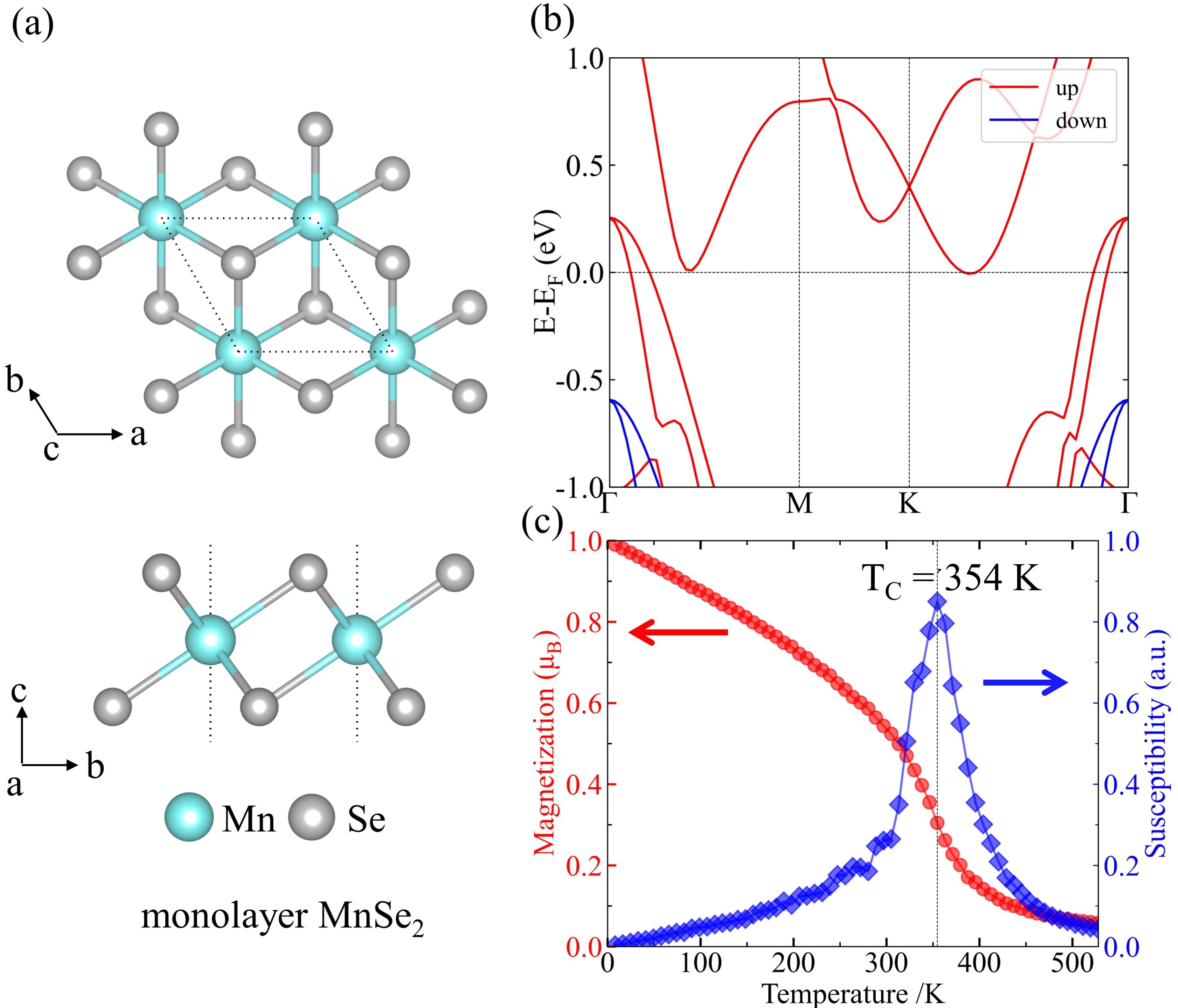
The crystal structure of monolayer MnSe2 is shown in Fig. 1(a), which shows a triangle lattice. The calculated in-plane lattice constant is = 3.658 Å, in agreement with previous calculations [62, 63, 64, 65]. The band structure of monolayer MnSe2 with HSE hybrid functional is shown in Fig. 1(b). The lowest band above Fermi level and the highest band below Fermi level slightly overlap, showing the semimetal behavior. The bands near Fermi level contain only one component of spins, showing the half-metal behavior. In addition, the Monte Carlo results of magnetization and susceptibility as a function of temperature for monolayer MnSe2 is shown in Fig. 1(c), giving a high = 354 K.
III.2 Monolayer MnSe2 with strain
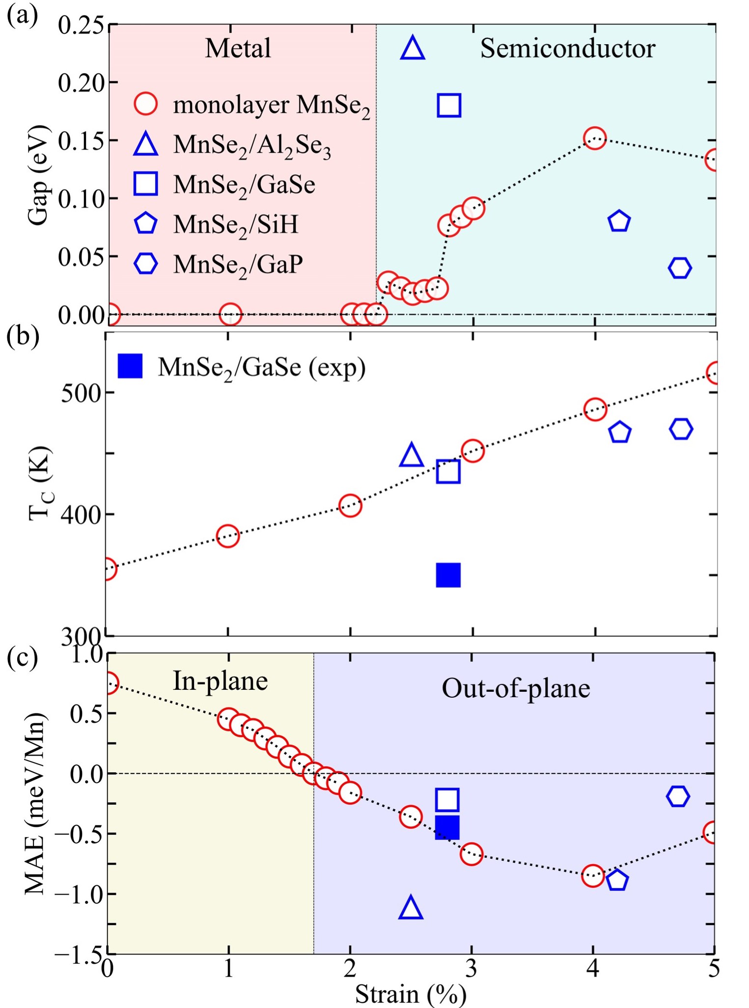
To study the effect of strain on electronic properties, we applied biaxial strain. The strain ratio is defined as , where and are the in-plane lattice constants with and without strain, respectively. The variation of band gap of monolayer MnSe2 with tensile strain calculated by DFT with HSE is shown in Fig. 2 (a). A metal-semiconductor transition happens with a tensile strain of 2.2%. Fig. 2 (b) shows of monolayer MnSe2 as a function with tensile strain. increase with tensile strain, in agreement with previous report [68, 38, 69, 70]. The MAE is defined as , where E⟂ and E∥ are energies of MnSe2 with out-of-plane and in-plane magnetic polarization, respectively. is the number of Mn atoms in a unit cell. For monolayer MnSe2 without strain, as shown in Fig. 2(c), the in-plane MAE of 0.75 meV/Mn is obtained, in agreement with the previous report [63]. By applying tensile strain, an in-plane to out-plane MAE transition is obtained at 1.7% tensile strain. Thus, monolayer MnSe2 will become a room temperature ferromagnetic semiconductor with out-of-plane MAE by applying tensile strains above 2.2%.
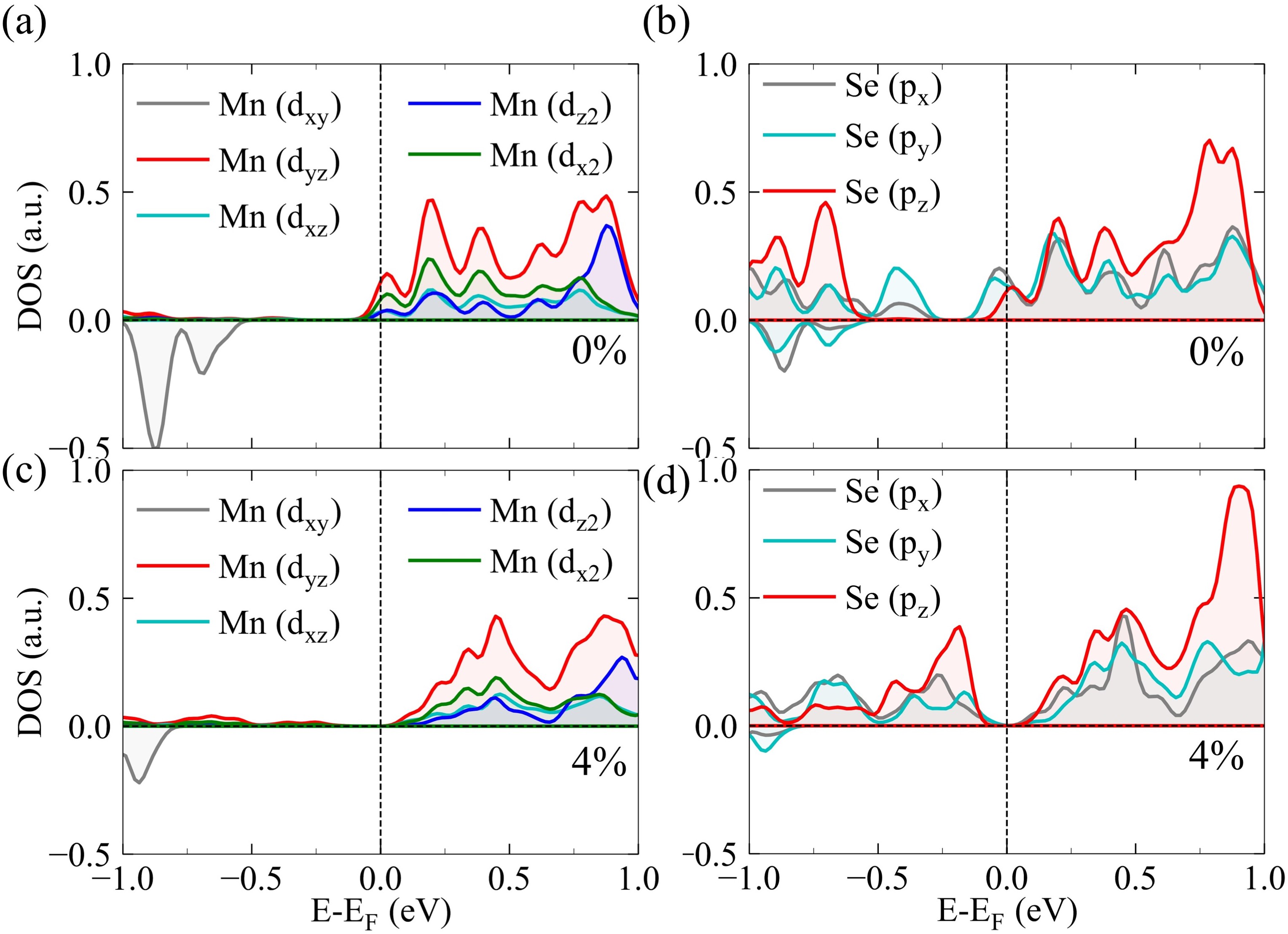
In order to analyze the metal-semiconductor transition of monolayer MnSe2 under strain, the partial density of states (PDOS) were calculated, as shown in Fig. 3. PDOS of d orbitals of Mn and p orbitals of Se without strain is shown in Figs. 3(a) and 3(b), respectively. PDOS of Mn and Se with 4% tensile strain is shown in Figs. 3(c) and 3(d), respectively, with a small gap. The tensile stains raise the energy of d orbitals of Mn atoms and p orbitals of Se atoms near the Fermi level, making the Fermi level lie in the energy gap of bonding and antibonding states of these p and d orbitals, and opening a small band gap.
III.3 Heterostructures MnSe2/X (X = GaP, GaSe, SiH, and Al2Se3)
Considering the mismatch from substrate is an efficient way to provide strain for 2D material in experiments [83], we constructed MnSe2-based heterostructures with 2D semiconductors to provide strain. GaP [71, 72], GaSe [74], SiH [75], and Al2Se3 [40] are nonmagnetic semiconductors. The calculated results with PBE at monolayer limit give band gaps of 1.22, 1.80, 2.18 and 1.69 eV, respectively, and lattice constants of 3.916, 3.814, 3.888 and 3.788 Å, respectively. According to the lattice mismatch , the lattice mismatch of GaP, GaSe, SiH, and Al2Se3 with MnSe2 are 6.8%, 4.2%, 6.1%, and 3.5%, respectively. The detailed results are given in Supplemental Material [84].
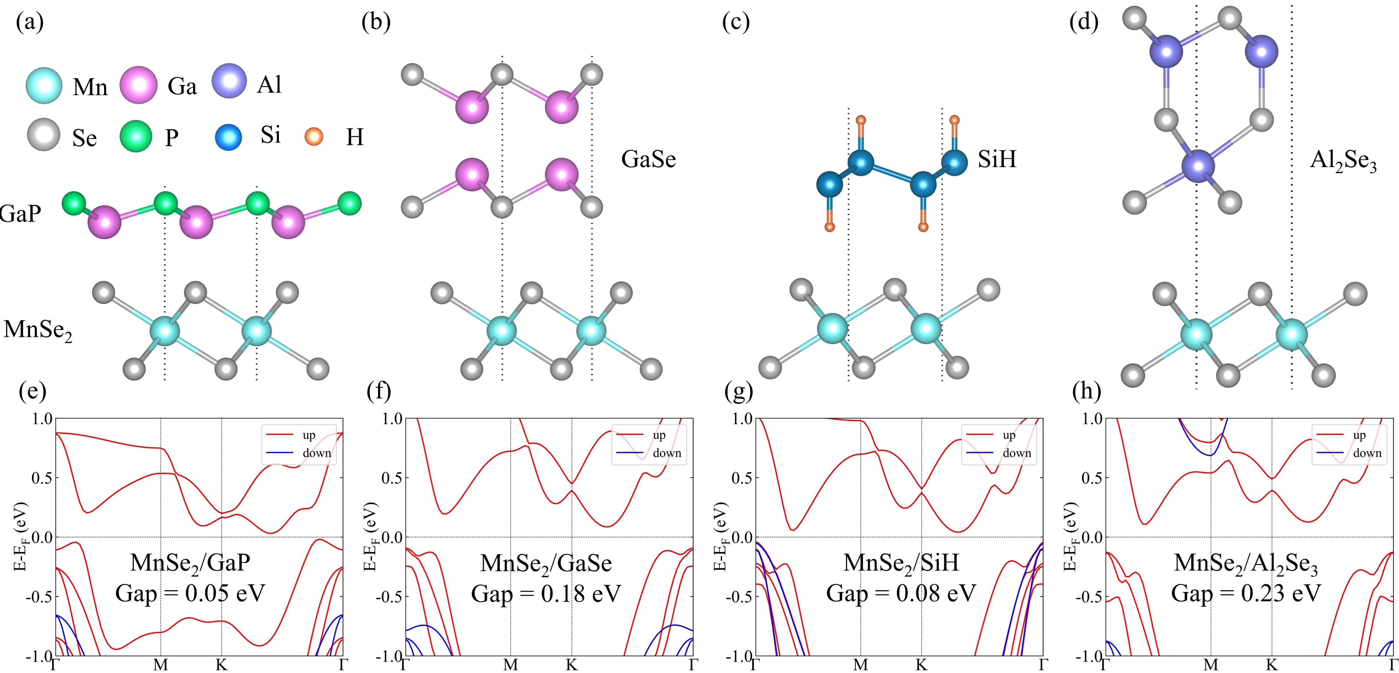
We consider different stacking models of heterostructures, and the detailed data are given in Supplemental Material [84]. As shown in Fig. 4, all heterostructures are ferromagnetic semiconductors. The optimised lattice constants of MnSe2/X with X = GaP, GaSe, SiH, and Al2Se3 are about 3.83, 3.76, 3.81, and 3.75 Å, respectively, with an effective tensile strain of 4.7%, 2.8%, 4.2%, and 2.5%, respectively. The binding energy for MnSe2/X is defined as , where , , and represent the total energies of heterostructure MnSe2/X, monolayer MnSe2, and monolayer X, respectively, and is the total atom number in a unitcell. The calculated results are -0.24, -0.17, -0.10, and -0.20 eV/atom for X = GaP, GaSe, SiH, and Al2Se3, respectively, indicating their stability. of heterostructures were obtained through DFT calculations and Monte Carlo simulation. As shown in Fig. 2, the calculation results predict that MnSe2/X with X = GaP, GaSe, SiH, and Al2Se3 are room temperature magnetic semiconductors with out-of-plane MAE. It is noted that for the heterostructure MnSe2/GaSe, Tc above room temperature and out-of-plane magnetization were observed in the experiment [19]. Thus, our calculation results in Fig. 2 are consistent with the experiment of MnSe2/GaSe [19]. The detailed calculation results are given in Supplemental Material [84].
Heterostructures not only provide effective strain, but also induce interlayer interaction. The calculated results of the most stable stacks of heterostructures is shown in Fig. 2. The calculated results of heterostructures are different with those of monolayer MnSe2 with the same tensile strain. For example, heterostructure MnSe2/GaSe has a band gap of 0.18 eV, while monolayer MnSe2 with same lattice constants has a band gap of 0.08 eV. Heterostructure MnSe2/Al2Se3 give a MAE of -1.11 meV/Mn, while monolayer MnSe2 with same lattice constants give a MAE of -0.36 meV/Mn. Therefore, the interlayer interaction may play an important role in properties of heterostructures.
III.4 MOKE in monolayer MnSe2 and heterostructures MnSe2/X
We investigated the magneto-optical Kerr effect for MnSe2 based structures. The Kerr rotation angle is given by:
| (1) |
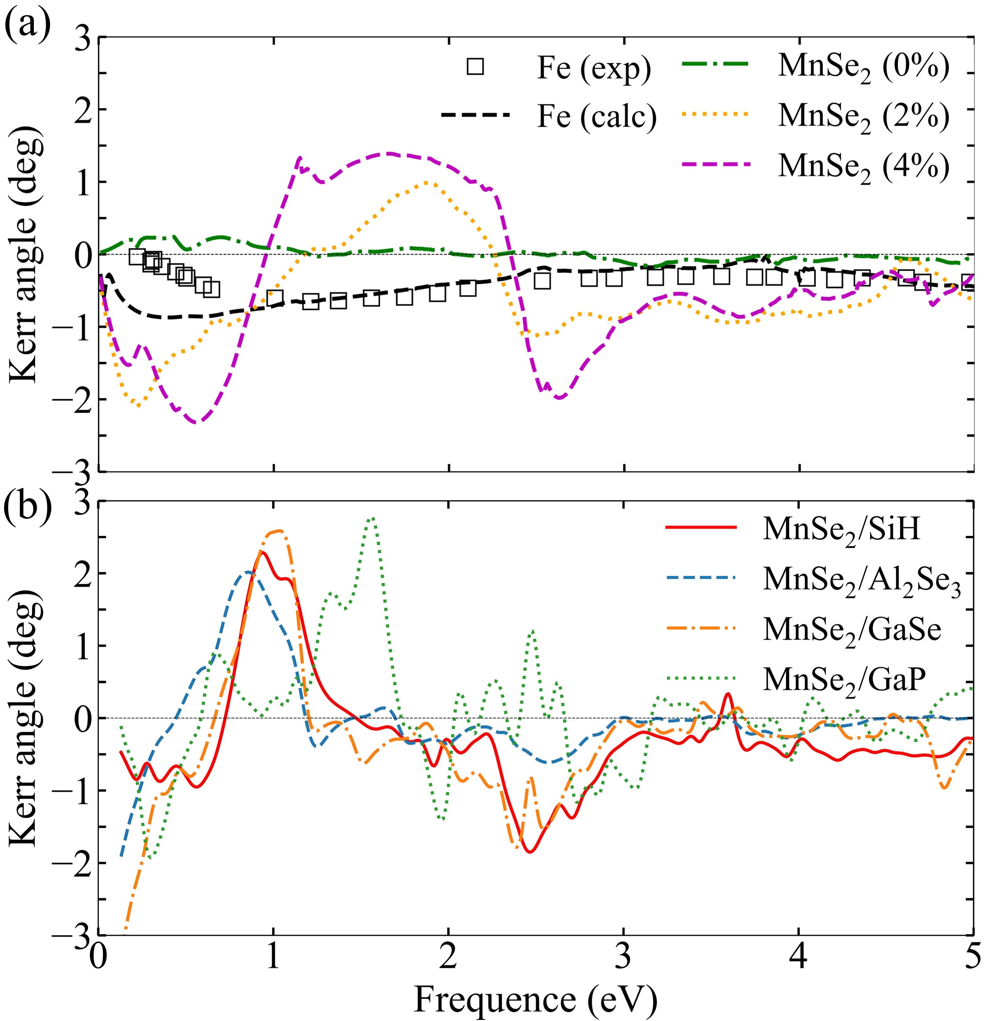
where and are the diagonal and off-diagonal components of the dielectric tensor , and is the frequency of incident light. The dielectric tensor can be obtained by the optical conductivity tensor as , where I is the unit tensor. The calculated Kerr rotation angle as a function of photon energy for monolayer MnSe2 with strain is shown in Fig. 5 (a), the result for heterostructures MnSe2/X with X = GaP, GaSe, SiH and Al2Se3 is shown in Fig. 5 (b). According to our calculation results, there exist large Kerr rotation angles with out-of-plane magnetization, such as monolayer MnSe2 with 2% and 4% tensile strain. On the contrary, Kerr rotation angles with in-plane magnetization are small, such as monolayer MnSe2 without strain. In addition, heterostructures MnSe2/X with out-of-plane magnetization also have a large Kerr rotation angle. The experimental result for Fe [85] and our DFT result for Fe bulk are also included for comparison. The Kerr rotation angles for stretched MnSe2 are about 4 times bigger than that of bcc Fe. Detailed results of Kerr rotation angles are given in Supplemental Material [84].
IV Conclusion
Based on the DFT calculations, we studied the properties of monolayer MnSe2 with strain and MnSe2-based heterostructures. For monolayer MnSe2, a metal-semiconductor transition happens at 2.2% tensile strain, and an in-plane to out-of-plane MAE transition happens at 1.7% tensile strain. In addition, of monolayer MnSe2 increases with tensile strain. The heterostructures MnSe2/X with X = GaP, GaSe, SiH, and Al2Se3 were studied, and the DFT calculation results show that they are room temperature ferromagnetic semiconductors with out-of-plane MAE. Large magneto-optical Kerr effect was found in monolayer MnSe2 with a few percent tensile strain and MnSe2-based heterostructures. Our results propose a way to obtain room temperature ferromagnetic semiconductors by metal-semicondutor transition in monolayer MnSe2 by applying a few percent tensile stain or building heterostructures.
V Acknowledgements
This work is supported by National Key R&D Program of China (Grant No. 2022YFA1405100), National Natural Science Foundation of China (Grant No. 12074378), Chinese Academy of Sciences (Grants No. YSBR-030, No. JZHKYPT-2021-08, No. XDB33000000), Beijing Municipal Science and Technology Commission (Grant No. Z191100007219013).
References
- Huang et al. [2017] B. Huang, G. Clark, E. Navarro-Moratalla, D. R. Klein, R. Cheng, K. L. Seyler, D. Zhong, E. Schmidgall, M. A. McGuire, D. H. Cobden, W. Yao, D. Xiao, P. Jarillo-Herrero, and X. Xu, Layer-dependent ferromagnetism in a van der Waals crystal down to the monolayer limit, Nat. 546, 270 (2017).
- Gong et al. [2017] C. Gong, L. Li, Z. Li, H. Ji, Alex Stern, Y. Xia, T. Cao, W. Bao, C. Wang, Y. Wang, Z. Q. Qiu, R. J. Cava, S. G. Louie, J. Xia, and X. Zhang, Discovery of intrinsic ferromagnetism in two-dimensional van der Waals crystals, Nat. 546, 265 (2017).
- Mermin and Wagner [1966] N. D. Mermin and H. Wagner, Absence of Ferromagnetism or Antiferromagnetism in One- or Two-Dimensional Isotropic Heisenberg Models, Phys. Rev. Lett. 17, 1307 (1966).
- Chu et al. [2019] J. Chu, Y. Zhang, Y. Wen, R. Qiao, C. Wu, P. He, L. Yin, R. Cheng, F. Wang, Z. Wang, J. Xiong, Y. Li, and J. He, Sub-millimeter-Scale Growth of One-Unit-Cell-Thick Ferrimagnetic Cr2S3 Nanosheets, Nano. Lett. 19, 2154 (2019).
- Cai et al. [2019] X. Cai, T. Song, N. P. Wilson, G. Clark, M. He, X. Zhang, T. Taniguchi, K. Watanabe, W. Yao, D. Xiao, M. A. McGuire, D. H. Cobden, and X. Xu, Atomically Thin CrCl3: An In-Plane Layered Antiferromagnetic Insulator, Nano. Lett. 19, 3993 (2019).
- Zhang et al. [2019a] Z. Zhang, J. Shang, C. Jiang, A. Rasmita, W. Gao, and T. Yu, Direct Photoluminescence Probing of Ferromagnetism in Monolayer Two-Dimensional CrBr3, Nano. Lett. 19, 3138 (2019a).
- Achinuq et al. [2021] B. Achinuq, R. Fujita, W. Xia, Y. Guo, P. Bencok, G. van der Laan, and T. Hesjedal, Covalent Mixing in the 2D Ferromagnet CrSiTe3 Evidenced by Magnetic X-Ray Circular Dichroism, Phys. Status. Solidi. 16, 2100566 (2021).
- Lee et al. [2021] K. Lee, A. H. Dismukes, E. J. Telford, R. A. Wiscons, J. Wang, X. Xu, C. Nuckolls, C. R. Dean, X. Roy, and X. Zhu, Magnetic Order and Symmetry in the 2D Semiconductor CrSBr, Nano. Lett. 21, 3511 (2021).
- Sun et al. [2022] S. Sun, J. Liang, R. Liu, W. Shen, H. Wu, M. Tian, L. Cao, Y. Yang, Z. Huang, W. Lin, J. Du, Z. Ni, Y. Xu, Q. Chen, and Y. Zhai, Anisotropic magnetoresistance in room temperature ferromagnetic single crystal CrTe flake, J. Alloy. Compd. 890, 161818 (2022).
- Meng et al. [2021] L. Meng, Z. Zhou, M. Xu, S. Yang, K. Si, L. Liu, X. Wang, H. Jiang, B. Li, P. Qin, P. Zhang, J. Wang, Z. Liu, P. Tang, Y. Ye, W. Zhou, L. Bao, H.-J. Gao, and Y. Gong, Anomalous thickness dependence of Curie temperature in air-stable two-dimensional ferromagnetic 1T-CrTe2 grown by chemical vapor deposition, Nat. Commun. 12, 94 (2021).
- Chua et al. [2021] R. Chua, J. Zhou, X. Yu, W. Yu, J. Gou, R. Zhu, L. Zhang, M. Liu, M. B. H. Breese, W. Chen, K. P. Loh, Y. P. Feng, M. Yang, Y. L. Huang, and A. T. S. Wee, Room Temperature Ferromagnetism of Monolayer Chromium Telluride with Perpendicular Magnetic Anisotropy, Adv. Mater. 33, 2103360 (2021).
- Li et al. [2022a] B. Li, X. Deng, W. Shu, X. Cheng, Q. Qian, Z. Wan, B. Zhao, X. Shen, R. Wu, S. Shi, H. Zhang, Z. Zhang, X. Yang, J. Zhang, M. Zhong, Q. Xia, J. Li, Y. Liu, L. Liao, Y. Ye, L. Dai, Y. Peng, B. Li, and X. Duan, Air-stable ultrathin Cr3Te4 nanosheets with thickness-dependent magnetic biskyrmions, Mater. Today 57, 66 (2022a).
- Zhang et al. [2019b] Y. Zhang, J. Chu, L. Yin, T. Shifa, Z. Cheng, R. Cheng, F. Wang, Y. Wen, X. Zhan, Z. Wang, and J. He, Ultrathin Magnetic 2D Single‐Crystal CrSe, Adv. Mater. 31, 1900056 (2019b).
- Deng et al. [2018] Y. Deng, Y. Yu, Y. Song, J. Zhang, N. Z. Wang, Z. Sun, Y. Yi, Y. Z. Wu, S. Wu, J. Zhu, J. Wang, X. H. Chen, and Y. Zhang, Gate-tunable room-temperature ferromagnetism in two-dimensional Fe3GeTe2, Nat. 563, 94 (2018).
- Fei et al. [2018] Z. Fei, B. Huang, P. Malinowski, W. Wang, T. Song, J. Sanchez, W. Yao, D. Xiao, X. Zhu, A. F. May, W. Wu, D. H. Cobden, J.-H. Chu, and X. Xu, Two-dimensional itinerant ferromagnetism in atomically thin Fe3GeTe2, Nat. Mater. 17, 778 (2018).
- Seo et al. [2020] J. Seo, D. Kim, E. An, K. Kim, G.-Y. Kim, S.-Y. Hwang, D. Kim, B. Jang, H. Kim, G. Eom, S. Seo, R. Stania, M. Muntwiler, J. Lee, K. Watanabe, T. Taniguchi, Y. Jo, J. Lee, B. Min, M. Jo, H. Yeom, S.-Y. Choi, J. Shim, and J. Kim, Nearly room temperature ferromagnetism in a magnetic metal-rich van der Waals metal, Sci. Adv. 6, eaay8912 (2020).
- May et al. [2019] A. May, D. Ovchinnikov, Q. Zheng, R. Hermann, S. Calder, B. Huang, Z. Fei, Y. Liu, X. Xu, and M. Mcguire, Ferromagnetism Near Room Temperature in the Cleavable van der Waals Crystal Fe5GeTe2, ACS Nano 13, 4436 (2019).
- Zhang et al. [2022] G. Zhang, F. Guo, H. Wu, X. Wen, L. Yang, W. Jin, W. Zhang, and H. Chang, Above-room-temperature strong intrinsic ferromagnetism in 2D van der Waals Fe3GaTe2 with large perpendicular magnetic anisotropy, Nat. Commun. 13, 5067 (2022).
- O’hara et al. [2018] D. O’hara, T. Zhu, A. Trout, A. Ahmed, Y. Luo, C. Lee, M. Brenner, S. Rajan, J. Gupta, D. Mccomb, and R. Kawakami, Room Temperature Intrinsic Ferromagnetism in Epitaxial Manganese Selenide Films in the Monolayer Limit, Nano. Lett. 18, 3125 (2018).
- Jiang et al. [2018] S. Jiang, L. Li, Z. Wang, K. F. Mak, and J. Shan, Controlling magnetism in 2D CrI3 by electrostatic doping, Nat. Nanotechnol. 13, 549 (2018).
- You et al. [2021] J.-Y. You, X.-J. Dong, B. Gu, and G. Su, Electric field induced topological phase transition and large enhancements of spin-orbit coupling and Curie temperature in two-dimensional ferromagnetic semiconductors, Phys. Rev. B 103, 104403 (2021).
- Zhao et al. [2021] F. Zhao, T. Cao, and S. G. Louie, Topological Phases in Graphene Nanoribbons Tuned by Electric Fields, Phys. Rev. Lett. 127, 166401 (2021).
- Shi et al. [2019] J. Shi, Y. Ou, M. A. Migliorato, H. Wang, H. Li, Y. Zhang, Y. Gu, and M. Zou, Tuning the electronic structure of GeC/WS2 van der Waals heterostructure by electric field and strain: A first principles study, Comput. Mater. Sci. 160, 301 (2019).
- Hao et al. [2019] Q. Hao, H. Yi, H. Su, B. Wei, Z. Wang, Z. Lao, Y. Chai, Z. Wang, C. Jin, J. Dai, and W. Zhang, Phase Identification and Strong Second Harmonic Generation in Pure -InSe and Its Alloys, Nano Lett. 19, 2634 (2019).
- Wang et al. [2018] B. Wang, Q. Wu, Y. Zhang, Y. Guo, X. Zhang, Q. Zhou, S. Dong, and J. Wang, High Curie-temperature intrinsic ferromagnetism and hole doping-induced half-metallicity in two-dimensional scandium chlorine monolayers, Nanoscale Horiz. 3, 551 (2018).
- Feng et al. [2017] S. Feng, Z. Lin, X. Gan, R. Lv, and M. Terrones, Doping two-dimensional materials: ultra-sensitive sensors, band gap tuning and ferromagnetic monolayers, Nanoscale Horiz. 2, 72 (2017).
- Fang et al. [2022] J. Fang, H. Song, B. Li, Z. Zhou, J. Yang, B. Lin, Z. Liao, and Z. Wei, Large unsaturated magnetoresistance of 2D magnetic semiconductor Fe-SnS2 homojunction, J. Semicond. 43, 092501 (2022).
- Zhao et al. [2022] D. Zhao, C. Zhang, C. Zhang, W. Ji, S. Li, and P. Wang, Magnetic tuning in a novel half-metallic Ir2TeI2 monolayer, J. Semicond. 43, 052001 (2022).
- González-Herrero et al. [2016] H. González-Herrero, J. M. Gómez-Rodríguez, P. Mallet, M. Moaied, J. J. Palacios, C. Salgado, M. M. Ugeda, J.-Y. Veuillen, F. Yndurain, and I. Brihuega, Atomic-scale control of graphene magnetism by using hydrogen atoms, Sci. 352, 437 (2016).
- Datta et al. [2017] S. Datta, Y. Cai, I. Yudhistira, Z. Zeng, Y.-W. Zhang, H. Zhang, S. Adam, J. Wu, and K. P. Loh, Tuning magnetoresistance in molybdenum disulphide and graphene using a molecular spin transition, Nat. Commun. 8, 94 (2017).
- Pathirage et al. [2023] V. Pathirage, S. Khatun, S. Lisenkov, K. Lasek, J. Li, S. Kolekar, M. Valvidares, P. Gargiani, Y. Xin, I. Ponomareva, and M. Batzill, 2D materials by Design: Intercalation of Cr or Mn between two VSe2 van der Waals Layers, Nano Lett. , e2004557 (2023).
- Zhou et al. [2021] J. Zhou, Z. Lin, H. Ren, X. Duan, I. Shakir, Y. Huang, and X. Duan, Layered Intercalation Materials, Adv. Mater. 33, 9579 (2021).
- Chen et al. [2019a] W. Chen, Z. Sun, Z. Wang, L. Gu, X. Xu, S. Wu, and C. Gao, Direct observation of van der Waals stacking-dependent interlayer magnetism, Sci. 366, 983 (2019a).
- Zhang et al. [2021a] X. Zhang, Q. Lu, W. Liu, W. Niu, J. Sun, J. CoOk, M. Vaninger, P. F. Miceli, D. J. Singh, S.-W. Lian, T.-R. Chang, X. He, J. Du, L. He, R. Zhang, G. Bian, and Y. Xu, Room-temperature intrinsic ferromagnetism in epitaxial CrTe2 ultrathin films, Nat. Commun. 12, 2492 (2021a).
- Kumar et al. [2016] P. Kumar, Y. S. Chauhan, A. Agarwal, and S. Bhowmick, Thickness and Stacking Dependent Polarizability and Dielectric Constant of Graphene-Hexagonal Boron Nitride Composite Stacks, J. Phys. Chem. C 120, 17620 (2016).
- Chen et al. [2023] Z. Chen, X. Liu, X. Li, P. Gao, Z. Li, W. Zhu, H. Wang, and X. Li, Large tunneling magnetoresistance in spin-filtering 1T-MnSe2/h-BN van der Waals magnetic tunnel junction, Nanoscale 15, 8447 (2023).
- Wu et al. [2023] B. Wu, J. Yang, S. Liu, S. Fang, Z. Liu, Z. Lin, J. Shi, W. Yang, Z. Luo, C. Wang, H. Du, J. Yang, and J. Lu, Layer-Dependent Magnetoresistance and Spin-Transfer Torque in MnSe2-Based Magnetic Tunnel Junctions, Phys. Rev. Applied 19, 064008 (2023).
- Dong et al. [2020] X.-J. Dong, J.-Y. You, Z. Zhang, B. Gu, and G. Su, Great enhancement of Curie temperature and magnetic anisotropy in two-dimensional van der Waals magnetic semiconductor heterostructures, Phys. Rev. B 102, 144443 (2020).
- Chen et al. [2019b] S. Chen, C. Huang, H. Sun, J. Ding, P. Jena, and E. Kan, Boosting the Curie Temperature of Two-Dimensional Semiconducting CrI3 Monolayer through van der Waals Heterostructures, J. Phys. Chem. C 123, 17987 (2019b).
- Li et al. [2023a] Y. Li, J. Deng, Y.-F. Zhang, X. Jin, W.-H. Dong, J.-T. Sun, J. Pan, and S. Du, Nonvolatile electrical control of spin polarization in the 2D bipolar magnetic semiconductor VSeF, npj Comput. Mater. 9, 50 (2023a).
- Ren et al. [2016] M. Ren, M. Li, C. Zhang, M. Yuan, P. Li, F. Li, W. Ji, and X. Chen, Band structures in silicene on monolayer gallium phosphide substrate, Solid State Commun. 239, 32 (2016).
- Caglayan et al. [2022] R. Caglayan, H. E. Guler, and Y. Mogulkoc, An analysis of Schottky barrier in silicene/Ga2SeS heterostructures by employing electric field and strain, Phys. Chem. Chem. Phys. 24, 10210 (2022).
- Yuan et al. [2022] G. Yuan, Z. Cheng, Y. Cheng, W. Duan, H. Lv, Z. Liu, C. Han, and X. Ma, Highly Sensitive Band Alignment of the Graphene/MoSi2N4 Heterojunction via an External Electric Field, ACS Appl. Electron. Mater. 4, 2897 (2022).
- Yuan et al. [2023] J. Yuan, F. Wang, Z. Zhang, B. Song, S. Yan, M.-H. Shang, C. Tong, and J. Zhou, Effects of electric field and interlayer coupling on Schottky barrier of germanene/MoSSe vertical heterojunction, Phys. Rev. B 108, 125404 (2023).
- Hong et al. [2022] J. Hong, C.-J. Kang, and J. Kim, Role of electronic correlations in room-temperature ferromagnetism of monolayer MnSe2, Phys. Rev. B 106, 195428 (2022).
- Yang et al. [2023] J. Yang, X. Wang, S. Li, X. Wang, M. Pan, M. Ai, H. Yuan, X. Peng, R. Wang, Q. Li, F. Zheng, and P. Zhang, Robust Two-Dimensional Ferromagnetism in Cr5Te8/CrTe2 Heterostructure with Curie Temperature above 400 K, ACS Nano , 23160 (2023).
- Zhu et al. [2023] W. Zhu, C. Song, L. Han, H. Bai, C. Chen, and F. Pan, Interface-enhanced room-temperature Curie temperature in CrPS4/graphene van der Waals heterostructure, Phys. Rev. B 108, l100406 (2023).
- Lu et al. [2023] X. Lu, Y. Deng, Y. Pei, Z. Chen, and G. Wang, Recent advances in NiO/Ga2O3 heterojunctions for power electronics, J. Semicond. 44, 061802 (2023).
- Huang et al. [2019] S. Huang, G. Zhang, F. Fan, C. Song, F. Wang, Q. Xing, C. Wang, H. Wu, and H. Yan, Strain-tunable van der Waals interactions in few-layer black phosphorus, Nat. Commun. 10, 94 (2019).
- Li et al. [2020] Z. Li, Y. Lv, L. Ren, J. Li, L. Kong, Y. Zeng, Q. Tao, R. Wu, H. Ma, B. Zhao, D. Wang, W. Dang, K. Chen, L. Liao, X. Duan, X. Duan, and Y. Liu, Efficient strain modulation of 2D materials via polymer encapsulation, Nat. Commun. 11, 94 (2020).
- Xu and Zhu [2018] Z. Xu and H. Zhu, Two-Dimensional Manganese Nitride Monolayer with Room Temperature Rigid Ferromagnetism under Strain, J. Phys. Chem. C 122, 14918 (2018).
- Wu et al. [2019] Z. Wu, J. Yu, and S. Yuan, Strain-tunable magnetic and electronic properties of monolayer CrI3, Phys. Chem. Chem. Phys. 21, 7750 (2019).
- Wei [2023] D. Wei, The room temperature ferromagnetism in highly strained two-dimensional magnetic semiconductors, J. Semicond. 44, 040401 (2023).
- Bertolazzi et al. [2011] S. Bertolazzi, J. Brivio, and A. Kis, Stretching and Breaking of Ultrathin MoS2, ACS Nano 5, 9703 (2011).
- Peng et al. [2014] R. Peng, H. C. Xu, S. Y. Tan, H. Y. Cao, M. Xia, X. P. Shen, Z. C. Huang, C. Wen, Q. Song, T. Zhang, B. P. Xie, X. G. Gong, and D. L. Feng, Tuning the band structure and superconductivity in single-layer FeSe by interface engineering, Nat. Commun. 5, 94 (2014).
- Zhang et al. [2016] P. Zhang, X.-L. Peng, T. Qian, P. Richard, X. Shi, J.-Z. Ma, B. B. Fu, Y.-L. Guo, Z. Q. Han, S. C. Wang, L. L. Wang, Q.-K. Xue, J. P. Hu, Y.-J. Sun, and H. Ding, Observation of high-TC superconductivity in rectangular FeSe/SrTiO3(110) monolayers, Phys. Rev. B 94, 104510 (2016).
- Cocco et al. [2010] G. Cocco, E. Cadelano, and L. Colombo, Gap opening in graphene by shear strain, Phys. Rev. B 81, 241412 (2010).
- Idrees et al. [2023] M. Idrees, M. Khurami, B. Amin, Y. Chen, and X. Yan, Interfacial characteristics, metal-semiconductor contact and optical properties of CSe and BX (X=B, As and Sb) monolayers, Mat. Sci. Semicon. Proc. 163, 107593 (2023).
- Hu and Ouyang [2021] H. Hu and G. Ouyang, First-principles calculations of interface engineering for 2D -In2Se3-based van der Waals multiferroic heterojunctions, Appl. Surf. Sci. 545, 149024 (2021).
- Noesges et al. [2020] B. A. Noesges, T. Zhu, J. J. Repicky, S. Yu, F. Yang, J. A. Gupta, R. K. Kawakami, and L. J. Brillson, Chemical migration and dipole formation at van der Waals interfaces between magnetic transition metal chalcogenides and topological insulators, Phys. Rev. Materials 4, 054001 (2020).
- Xiao et al. [2023] C. Xiao, W. Wu, H. Wang, Y.-X. Huang, X. Feng, H. Liu, G.-Y. Guo, Q. Niu, and S. A. Yang, Time-Reversal-Even Nonlinear Current Induced Spin Polarization, Phys. Rev. Lett. 130, 166302 (2023).
- Eren et al. [2019] I. Eren, F. Iyikanat, and H. Sahin, Defect tolerant and dimension dependent ferromagnetism in MnSe2, Phys. Chem. Chem. Phys. 21, 16718 (2019).
- Xie et al. [2021] W.-Q. Xie, Z.-W. Lu, C.-C. He, X.-B. Yang, and Y.-J. Zhao, Theoretical study of tunable magnetism of two-dimensional MnSe2 through strain, charge, and defect, J. Phys.: Condens. Matter 33, 215803 (2021).
- Li et al. [2022b] Q. Li, C. xin Zhang, D. Wang, K.-Q. Chen, and L.-M. Tang, Giant valley splitting in a MoTe2/MnSe2 van der Waals heterostructure with room-temperature ferromagnetism, Mater. Adv. 3, 2927 (2022b).
- Kan et al. [2014] M. Kan, S. Adhikari, and Q. Sun, Ferromagnetism in MnX2 (X = S, Se) monolayers, Phys. Chem. Chem. Phys. 16, 4990 (2014).
- He et al. [2022] J. He, S. Li, L. Zhou, and T. Frauenheim, Ultrafast Light-Induced Ferromagnetic State in Transition Metal Dichalcogenides Monolayers, J. Phys. Chem. Lett. 13, 2765 (2022).
- Heyd et al. [2003] J. Heyd, G. E. Scuseria, and M. Ernzerhof, Hybrid functionals based on a screened Coulomb potential, J. Chem. Phys. 118, 8207 (2003).
- Dong et al. [2019] X.-J. Dong, J.-Y. You, B. Gu, and G. Su, Strain-Induced Room-Temperature Ferromagnetic Semiconductors with Large Anomalous Hall Conductivity in Two-Dimensional Cr2Ge2Se6, Phys. Rev. Appl. 12, 014020 (2019).
- Zhang et al. [2021b] Z. Zhang, J.-Y. You, X.-Y. Ma, B. Gu, and G. Su, Kagome quantum anomalous Hall effect with high Chern number and large band gap, Phys. Rev. B 103, 014410 (2021b).
- O’Neill et al. [2022] A. O’Neill, S. Rahman, Z. Zhang, P. Schoenherr, T. Yildirim, B. Gu, G. Su, Y. Lu, and J. Seidel, Enhanced Room Temperature Ferromagnetism in Highly Strained 2D Semiconductor Cr2Ge2Te6, ACS Nano 17, 735 (2022).
- Li et al. [2022c] H. Li, Y. Liu, Z. Bai, J. Xiong, F. Liu, G. Zhou, T. Qing, S. Zhang, and J. Lu, Ohmic contact in graphene and hexagonal III-V monolayer (GaP, GaAs, InP, and InAs) van der Waals heterostructures: Role of electric field, Phys. Lett. A 433, 128029 (2022c).
- Parmar et al. [2022] P. Parmar, S. Khengar, and P. Thakor, Structural And Electronic Properties of PtSe2/GaP Heterostructure, Mater. Today:. Proc. 67, 161 (2022).
- Wei et al. [2022] T. Wei, X. Li, Z. Li, W. Yang, Y. Wu, Z. Xing, and S. Lu, Interfacial dynamics of GaP/Si(100) heterostructure grown by molecular beam epitaxy, J. Semicond. 43, 122101 (2022).
- Li et al. [2023b] W. Li, X. Zhang, J. Yang, S. Zhou, C. Song, P. Cheng, Y.-Q. Zhang, B. Feng, Z. Wang, Y. Lu, K. Wu, and L. Chen, Emergence of ferroelectricity in a nonferroelectric monolayer, Nat. Commun. 14, 2757 (2023b).
- Wani et al. [2022] A. F. Wani, B. Rani, S. Dhiman, U. B. Sharopov, and K. Kaur, Sih monolayer: A promising two-dimensional thermoelectric material, Int. J. Energ. Res. 46, 10885 (2022).
- Kresse and Furthmüller [1996] G. Kresse and J. Furthmüller, Efficient iterative schemes for ab initio total-energy calculations using a plane-wave basis set, Phys. Rev. B 54, 11169 (1996).
- Perdew et al. [1996] J. P. Perdew, K. Burke, and M. Ernzerhof, Generalized Gradient Approximation Made Simple, Phys. Rev. Lett. 77, 3865 (1996).
- Blöchl [1994] P. E. Blöchl, Projector augmented-wave method, Phys. Rev. B 50, 17953 (1994).
- Grimme et al. [2010] S. Grimme, J. Antony, S. Ehrlich, and H. Krieg, A consistent and accurate ab initio parametrization of density functional dispersion correction DFT-D for the 94 elements H-Pu, J. Chem. Phys. 132, 154104 (2010).
- Mostofi et al. [2008] A. A. Mostofi, J. R. Yates, Y.-S. Lee, I. Souza, D. Vanderbilt, and Nicola Marzari, wannier90: A tool for obtaining maximally-localised Wannier functions, Comput. Phys. Commun. 178, 685 (2008).
- Mostofi et al. [2014] A. A. Mostofi, J. R. Yates, G. Pizzi, Y.-S. Lee, I. Souza, D. Vanderbilt, and Nicola Marzari, An updated version of wannier90: A tool for obtaining maximally-localised wannier functions, Comput. Phys. Commun. 185, 2309 (2014).
- Wu et al. [2018] Q. Wu, S. Zhang, H.-F. Song, M. Troyer, and Alexey A. Soluyanov, Wanniertools: An open-source software package for novel topological materials, Comput. Phys. Commun. 224, 405 (2018).
- Qi et al. [2023] Y. Qi, M. A. Sadi, D. Hu, M. Zheng, Z. Wu, Y. Jiang, and Y. P. Chen, Recent Progress in Strain Engineering on Van der Waals 2D Materials: Tunable Electrical, Electrochemical, Magnetic, and Optical Properties, Adv. Mater. 35, 2205714 (2023).
- [84] See supplemental material .
- Oppeneer et al. [1992] P. M. Oppeneer, T. Maurer, J. Sticht, and J. Kübler, Ab initio calculated magneto-optical Kerr effect of ferromagnetic metals: Fe and Ni, Phys. Rev. B 45, 10924 (1992).