Siracusa: A 16 nm Heterogenous RISC-V SoC for Extended Reality with At-MRAM Neural Engine
Abstract
Extended reality (XR) applications are Machine Learning (ML)-intensive, featuring deep neural networks (DNNs) with millions of weights, tightly latency-bound (10-20 ms end-to-end), and power-constrained (low tens of mW). While ML performance and efficiency can be achieved by introducing neural engines within low-power systems-on-chip (SoCs), system-level power for nontrivial DNNs depends strongly on the energy of non-volatile memory (NVM) access for network weights. This work introduces Siracusa, a near-sensor heterogeneous SoC for next-generation XR devices manufactured in 16 nm CMOS. Siracusa couples an octa-core cluster of RISC-V digital signal processing cores with a novel tightly-coupled “At-Memory” integration between a state-of-the-art digital neural engine called N-EUREKA and an on-chip NVM based on magnetoresistive memory (MRAM), achieving 1.7 higher throughput and 4.1 better energy efficiency than XR SoCs using MRAM as background memory. The fabricated SoC prototype achieves an area efficiency of 65.2 GOp/s/mm and a peak energy efficiency of 8.84 TOp/J for DNN inference while supporting complex, heterogeneous application workloads, which combine ML with conventional signal processing and control.
I Introduction
The effort to create an immersive approach for interacting with digital content is fueling the growth of Extended Reality (XR) applications in various sectors, including healthcare, education, and training. XR applications can potentially revolutionize our approach to interact with digital content [1] through seamless interaction with digital and real objects through context-aware processing, integrating natural user expressions with advanced algorithms.
Previous generations of Virtual Reality (VR) devices are bulky and offload most of their compute-intensive tasks to remote servers or personal gateways. In contrast, the next generation of XR glasses will need to deliver competitive real-time performance in a lightweight, non-stigmatizing ”classic eyeglass” form factor [1]. However, there are several challenges to designing non-stigmatizing XR glasses in addition to the miniaturization of electronics and tight integration of sensors and processors. Most importantly, XR glasses must process sensor inputs in real-time to convert, among others, gestures, speech, and user gaze [2, 3, 1] into actionable information. Furthermore, battery lifetime is a crucial design challenge; XR glasses should last throughout a day of continuous use without requiring large and heavy battery packs.
A promising approach to overcome several key challenges of future XR glasses is near-sensor or edge computing; processing data close to its source minimizes the latency between sampling and reacting to user input while reducing or eliminating the energy required to transfer high-bandwidth sensor data to remote servers, which represents a large share of power consumption in this class of devices [1]. Additionally, privacy concerns are minimized by transmitting only highly compressed, non-personally identifiable sensor data from the near-sensor computing system.
While the promises of near-sensor computing are enticing, there are several practical challenges to leverage its advantages. A significant challenge of near-sensor XR compute systems lies in balancing the performance and efficiency of classic computer vision workloads with modern Deep Neural Network (DNN)-based data extraction. A common approach is to integrate core-based compute clusters with DNN accelerators [4, 5, 6, 7, 8]. This approach enables high energy efficiency and throughput for critical tasks based on DNNs, such as hand or eye tracking, while preserving general-purpose computing capabilities. However, efficient collaboration of cores and accelerators is a complex design challenge. Unless cores and accelerators are tightly integrated through high-bandwidth shared memory, end-to-end performance suffers from added latency and energy consumption caused by extensive data movement between cores and accelerators.
Another major challenge for edge computing systems in the XR domain is efficient data movement, especially regarding loading neural network weights. Different strategies have been proposed to address this bottleneck, the most promising of which is the introduction of high-density Non-volatile Memory (NVM) on the chip, but conventional Flash NVM cannot be integrated into scaled FinFET technologies. Emerging Magnetoresistive Random Access Memory (MRAM) technology achieves comparable speed and read energy-per-access to Static Random Access Memory (SRAM) at significantly higher density and is compatible with back end of line (BEOL) fabrication in FinFET processes [9, 10]. As such, MRAM opens up many integration opportunities in heterogeneous Systems-on-Chip (SoCs): emerging In-Memory Computing (IMC) approaches merge NVM with the accelerator, but must trade-off with storage density or compute precision, impacting the end-to-end performance of the system. On the other hand, integrating NVMs as background (L2/L3) on-chip memory optimizes density at a significant price in access bandwidth, latency, and, ultimately, energy efficiency.
In this work, we extend our ESSCIRC’23[11] paper presenting Siracusa, an all-digital SoC for XR computing fabricated in TSMC 16 nm. Siracusa introduces a novel architecture for tightly-coupled NVM integration with our accelerator, N-EUREKA, enabling high access speed (9-cycle latency, 92 Gbit/s) without overheads in terms of storage density or readout efficiency. We call our approach ”at” MRAM to distinguish it from ”in” memory solutions, as it provides a new design point in the trade-off between accelerator energy efficiency and memory density. Furthermore, by coupling the At-MRAM N-EUREKA engine with a cluster of RISC-V cores via a low-latency interconnect and shared multi-banked SRAM, our design enables efficient, zero-copy, collaborative execution of heterogeneous Machine Learning (ML), Digital Signal Processing (DSP), and control workloads while maximizing end-to-end energy efficiency.
Specifically, the contributions of this paper are as follows:
-
•
We introduce a novel At-MRAM computing architecture where NVM is tightly coupled with compute engines that uses of high-density, high-bandwidth, non-volatile on-chip MRAM for DNN weights, eliminating off-chip weight transfers for standard edge computing DNNs. We demonstrate that our design reduces DNN inference latency by 40 % and increases end-to-end energy efficiency by 4.1 compared to conventional (L3) NVM integration schemes, which use NVM as background memory.
-
•
In addition to the non-volatile MRAM, we integrate a SRAM tile memory, which minimizes feature map data movement between hierarchy levels. For networks larger than , the proposed tile memory can be used as additional high bandwidth weight memory using a novel lightweight hardware page manager, allowing it to switch between weight pages seamlessly.
-
•
We present a heterogeneous compute cluster architecture integrating At-MRAM N-EUREKA, a cooperative, weight-precision-tunable Convolutional DNN accelerator featuring a peak DNN inference performance of with a state-of-the-art octa-core RISC-V Cluster through a heterogeneous interconnect, enabling priority-based bandwidth sharing of the Cluster’s L1 memory.
The rest of this paper is organized as follows: in Section II, we discuss the SoC architecture of Siracusa. Section III presents measurement results and details Siracusa’s performance characteristics on representative XR workloads. Section IV discusses the impact of tightly integrating NVM with our accelerator and compares our design to conventional integration approaches. In Section V, we compare our work to the previous state-of-the-art. Finally, Section VI concludes this article, summarizing the results.
II Architecture
In this section, we introduce the hardware architecture of Siracusa. Furthermore, we demonstrate how the tight coupling of NVM with the system’s main DNN compute engine enables ultra-efficient zero-off-chip transfer inference of state-of-the-art XR workloads.

The Siracusa SoC comprises two domains: The IO-Domain and the Heterogeneous Cluster as shown in Figure 1. The IO-Domain consists of an advanced microcontroller based on a 32-bit RISC-V Fabric Controller (FC) core responsible for management tasks, using the RV32IMC instruction set with Xpulp Instruction Set Architecture (ISA) extensions. The Xpulp extensions enhance throughput with zero-overhead hardware loops, post-increment load-store instruction, fixed-point operations, bit manipulations, and dot product instructions for 16-bit and 8-bit data.
The IO-Domain includes a large L2 SRAM scratchpad memory divided into four word-interleaved banks. An additional memory is reserved for the FC program code and stack. The boot code for the core is stored in a dedicated boot ROM.
The IO-Domain incorporates an IO-Direct Memory Access (DMA) controller to transfer data between the L2 memory and IO interfaces efficiently. The supported IO interfaces include SPI, I3C, HyperRAM, and UART, as well as a dedicated camera interface with the image sensor to be tightly integrated for near-sensor computing [1][12]. This rich set of IO interfaces enhances Siracusa’s adaptability and versatility to a diverse group of external devices, thus enabling its usability in various applications. The IO-Domain contains three individual PLLs to generate clocks for the IO-Domain, Cluster and the IO-Peripherals. The FC accesses the PLLs, GPIOs, Debug Unit, and timers via a 32-bit APB crossbar. The Cluster is located in a separate power and frequency domain, consisting of 8 RISC-V cores, a Convolutional Neural Network (CNN) accelerator, N-EUREKA, and a tightly coupled Neural Memory Subsystem. The IO-Domain and the Cluster are connected via a Clock Domain Crossing (CDC) into the 64-bit AXI Cluster interconnect.
II-A Heterogeneous Cluster
The Heterogeneous Cluster is an Artificial Intelligence (AI) and DSP accelerator organized around two cooperative engines: a parallel set of 8 RISC-V cores tailored to DSP tasks, and a specialized hardware engine for quantized DNN inference, called N-EUREKA.
The 8 RISC-V cores utilize the RV32IMCF ISA, similar to the FC. Furthermore, the cores are enhanced with the Xpulpnn instruction set, a superset of Xpulp adding support for dot-product for sub-byte 2, 4, 8-bit data and enhanced MAC&LOAD instructions overlapping data loading with computation [4]. The RISC-V cores achieve near-100% Multiply-Accumulate (MAC) utilization for linear algebra-dominated kernels, such as matrix multiplications and linear transformations. The cores also support floating-point instructions via a dedicated Floating Point Unit (FPU). In addition to the single-precision standard extension F, the floating point units support short-float formats such as FP8, FP16, FP16Brain [13], catering to the needs of a diverse range of visual processing applications with different properties in terms of quantization noise resilience; in Siracusa, we employed a configuration with one private floating point unit per core using two pipeline stages. A detailed discussion of the compute cluster design and performance measurements may be found in Montagna et al. [13].
The RISC-V cores are equipped with a hierarchical instruction cache (I$) implemented with , 4-way associative, shared among all 8 cores and one dedicated 4-way associative cache per core [14]. The I$ is implemented with Standard Cell Memories (SCMs) to enable multiport access efficiently compared to regular SRAM cuts.
Along with the RISC-V cores, the Cluster domain also includes N-EUREKA, a configurable hardware accelerator designed to perform DNN inference tasks efficiently. N-EUREKA supports 33 dense, 33 depthwise, and 11 dense convolutions with 8-bit activation and configurable weight precision from 2-8 bits. The internal architecture of N-EUREKA is described in greater detail in Section II-C. Alongside the two main compute engines, the Cluster includes many auxiliary peripherals, such as a DMA controller and an event unit, which helps orchestrate high-performance parallel execution of the RISC-V cores and concurrent DMA transfers. The RISC-V cores configure the DMA, Event Unit, and N-EUREKA via a 32-bit peripheral interconnect.
To support the execution of cooperative tasks, the RISC-V cores and N-EUREKA share a single L1 Tightly-coupled Data Memory (TCDM) organized into 16 word-interleaved banks. The TCDM is accessible via a low-latency L1 interconnect enabling access to the TCDM at an aggregate bandwidth up to at . In the absence of bank contention, accesses are performed in a single cycle of latency. The shared nature of L1 memory access mitigates superfluous data movements and enables pipelined, collaborative execution of tasks on N-EUREKA and the RISC-V cores, maximizing performance and efficiency.
The low latency L1 interconnect is organized hierarchically into a logarithmic and a shallow branch. The logarithmic branch is used for arbitration between the 8 RISC-V cores, the DMA, and as an external port towards the IO-Domain. The accesses are routed to each memory bank; the logarithmic branch employs a bank-level round-robin arbitration scheme in the event of memory contentions, thus avoiding core starvation. In contrast, the shallow branch from N-EUREKA routes accesses from a single contiguous-by-construction high bandwidth () N-EUREKA port towards the L1 memory banks, without any bank-wise arbitration. The accesses of each of the two branches to the SRAM TCDM banks are further arbitrated using a configurable priority arbitrator without starvation, which can guarantee a minimum share of bandwidth for either branch while maximizing access bandwidth for the other [15].
II-B Neural Memory Subsystem
In addition to L1 TCDM memory, the Siracusa Cluster also introduces a dedicated Neural Memory Subsystem to enable the At-Memory acceleration concept discussed in Section I.
II-B1 Weight MRAM and tile SRAM subsystems
The Neural Memory Subsystem is synchronous at the interface to the rest of the Cluster and comprises two distinct subsystems. The first subsystem is a novel weight memory subsystem implemented using non-volatile MRAM. It is exclusively dedicated to storing DNN weights, which are accessible to the N-EUREKA accelerator contention-free and at high bandwidth, with a tight integration scheme detailed in Section II-C. The MRAM is organized internally in four banks of each, which reside in a dedicated frequency/voltage domain, isochronous to the rest of the Cluster through a clock divider defaulting to 1/2 setting. Each bank is divided into two 512 KiB cuts accessible in parallel (for a total bandwidth of up to 512 bits/cycle @ 180 MHz) to provide the required bandwidth for N-EUREKA while coping with the divided clock.
The second subsystem in the Neural Memory Subsystem is the tile memory subsystem, implemented using conventional SRAM. The primary role of this volatile memory is to store intermediate feature map tiles without relying on the IO-Domain L2 and using the IO-Domain-Cluster CDC. As a secondary purpose, this memory could also be used for additional (temporary) storage of weights streamed from off-chip Flash for DNNs with a larger memory footprint than the available on-chip MRAM, to allow scalability of the workload at the cost of performance, or for weights that are frequently field-tuned during system operation (e.g., for continuous learning applications [16]).
Both subsystems share a single 64-bit AXI read and write port to the Cluster interconnect (up to @ ) used to access the Neural Memory Subsystem from the Cluster through the AXI interconnect for MRAM configuration, initial weight programming, activation load/store access, and general use from the Cluster’s cores. A wide (256-bit, up to @ ) read-only port provides the At-Memory access from the accelerator at high bandwidth and contention-free, with only nine cycles of access latency. Section II-C4 discusses the pipelining scheme employed by N-EUREKA to access the weight memory subsystem at high bandwidth, while an in-depth discussion of the weight memory subsystem, comparing it to several state-of-the-art alternatives, is included in Section IV.
II-B2 Software-assisted virtual memory paging
Optionally, the Neural Nemory Subsystem can operate in a lightweight, software-assisted virtual memory mode where N-EUREKA operates on virtual \qty4\mebi pages. This mode provides complete functionality when running larger networks, which require more than . In this mode, Siracusa must use an off-chip background memory and use the system IO-Domain L2 memory to hold intermediate activations. In the virtual memory mode, the Neural Memory Subsystem is used as a cache for memory pages of the DNN weights allocated in off-chip Flash. A small page handling circuitry maps N-EUREKA’s transaction to either of the two physical memory pages (residing in the tile SRAM and weight MRAM, respectively) by comparing the address prefix with the two live page index registers that are exposed via the Neural Memory Subsystem’s configuration interface.
Unless a transaction’s page index matches either index register, it is stalled, and a page-miss interrupt is raised towards the FC, which programs the IO-DMA to perform a weight page swap through the 32-bit AXI CDC. This happens concurrently with L2-L1 DMA transfers, which can support tiling of activations via the separate 64-bit CDC port.
Once finished, the FC updates the page index register, unblocking the stalled transaction, which is completely transparent to N-EUREKA. The system also supports proactive page swapping that takes advantage of the typically deterministic weight access pattern in DNN workloads. Such a swapping can be triggered by the FC on a page-switch interrupt, which allows for transparent network reconfiguration with negligible increase in overall circuit area and minimizes stall time.
II-C N-EUREKA
Given the pervasiveness of DNNs in modern XR pipelines [1, 7], one of the design goals of Siracusa is state-of-the-art energy-efficient neural network inference acceleration. To effectively exploit the advantages of modern quantized neural networks, N-EUREKA supports integer mixed-precision inference. This Section introduces the working principle and architecture of N-EUREKA and highlights the close integration of the MRAM weight memory.
II-C1 Operating principle
N-EUREKA is a programmable hardware accelerator that supports 33 dense, 33 depthwise, and 11 dense convolutions. It supports 8-bit input activation, 2-8-bit weight precision, and 8-bit requantized or 32-bit outputs. N-EUREKA’s datapath is designed for bit-serial arithmetic, performing higher bit-width product calculations using bit shifting and repeated addition. N-EUREKA performs 33 dense and depthwise convolution in a bit serial manner, whereas it exploits the adder and shifter to perform 11 dense convolution in a bit parallel mode. Requantization is achieved by an integer-domain affine projection: N-EUREKA uses per-channel scaling, bias, and shift parameters, which are applied according to the requantization scheme proposed by Conti [17].

II-C2 Microarchitecture
Figure 2 shows the architecture of N-EUREKA. We divide the architecture into three main components: two streamers, a controller, and a datapath unit. The controller consists of a latch-based dual context register file programmable by any RISC-V core in Siracusa through the peripheral interconnect. N-EUREKA hosts two streamers: an L1 streamer, which provides 288-bit load / store access to L1 memory via the TCDM interconnect, and a weight streamer, toward the Neural Memory Subsystem. The L1 streamer is time division multiplexed to load input activations, normalization parameters, and optionally weights and to store processed output activation. Both streamers internally support the same bandwidth of of contiguous data per cycle in either direction. The available bandwidth is constrained by the available MRAM bandwidth as explained in Section II-C4; the same bandwidth is used in the shallow L1 interconnect to simplify the accelerator’s control. To handle the case of data that are not aligned on a word boundary in word-interleaved memory, N-EUREKA’s L1 memory interface can load or store up to of data from contiguous banks. The accelerator’s L1 streamer automatically selects the relevant 256 bits from this larger block. Fetching an extra word to compensate for unaligned accesses is necessary for L1 data, as they could be produced by the RISC-V cores; it is not required for the weight streamer, which accesses weight data that is aligned by construction. Equipped with support for three-dimensional strided address generation, both streamers can serialize any 3D data access pattern and convert them to memory access transactions.
N-EUREKA’s datapath consists of SCM-based InputBuffers to store 8832 input activation tiles and 66 PEs, allowing the accelerator to process 88 spatial dimension tiles. Each PE consists of 288 18 bit multipliers organized into 9 rows and 32 columns. Each PE also has 3232-bit accumulators to store partial sums. One additional NormQuantUnit per PE performs scaling, adding a bias, and right-shifting, which are used to requantize higher bit-width outputs to 8 bits.
II-C3 Execution

N-EUREKA’s execution starts when a RISC-V core offloads a task via configuring a dedicated memory-mapped register. The register file is designed to support queueing two tasks, eliminating extraneous latency due to configuration overhead when running multiple tasks back-to-back. N-EUREKA’s execution is handled via a Finite State Machine (FSM), which controls the dispatch of tile computations on PEs.
The execution flow of N-EUREKA follows an output stationary and quasi-input stationary pattern, similar to [4]. The activation layout used by N-EUREKA is HWC111Pixels are laid out in memory so that consecutive channels are adjacent; blocks of pixels corresponding to all channels in a given spatial position are laid out in row-major format. in L1 memory, and weights are packed into 256-bit blocks. The execution starts with the prefetch state by loading 328-bit activation per cycle from L1 memory and storing it in the InputBuffer. At the end of the prefetch state, the activations are assigned to the multiplier units of all PEs using the DispatchingNetwork. Next, the execution state begins with a access to the Neural Memory Subsystem via the weight streamer. The weights fetched are broadcast to all 66 PEs, allowing the reuse of weights in the spatial dimension. Using the Neural Memory Subsystem to store the DNN weights frees the bandwidth towards the L1 memory in the execution state. This bandwidth is exploited to prefetch the next activation tile to the second input buffer. This overlap of the prefetch and execution state allows the accelerator to hide the latency of fetching subsequent tiles.
In dense convolution execution, the partial sum is accumulated in the 3232-bit accumulators. Once all input tiles in the channel dimension for one spatial tile of a convolution have been processed, the partial sum in the accumulators undergoes the normalization and quantization phase. Then, in the streamout state, the normalized and quantized output stored in the accumulators is written back to the L1 memory via the L1 streamer. This process is repeated for all remaining spatial input tiles.
II-C4 Weight Memory Subsystem Integration
While conventional memory technologies like SRAM are designed to support high-frequency memory accesses without practical limits on their memory cell lifetime, the write endurance of Spin Transfer Torque (STT) MRAM is limited [18, 19]. Moreover, its write process is orders of magnitude slower than SRAM, taking tens of nanoseconds [18]. Additionally, read access times for STT-MRAM are typically in the range of [10] which corresponds to an operating frequency of , which is much lower than the operating frequency of state-of-the-art accelerators [4, 20], making direct integration with high-throughput computing systems like N-EUREKA challenging. The proprietary MRAM macro integrated into Siracusa is designed for read access operation at up to .
In Siracusa, we address MRAM’s slow write performance and limited write endurance by integrating it as a static DNN weight memory coupled to the accelerator rather than a conventional read-write cache. By dimensioning the weight memory subsystem with enough capacity to hold all weights of state-of-the-art XR DNNs and exploiting its non-volatility, we avoid write accesses to the MRAM at runtime. Similarly, we address the MRAM IP’s slower-than-SRAM read performance by pipelining two word-interleaved memory banks at half the accelerator’s clock frequency, as shown in Figure 3; the banks are accessed in parallel during an MRAM clock cycle (for a total bandwidth of 512 bits/cycle @ 180 MHz). The DNN weights are laid out so that the accesses happen in long streams of adjacent addresses, making it possible to hide the access latency of the MRAM cuts due to the analog access time and three internal pipeline stages, as shown in Fig. 3, on the left.
Following the At-Memory paradigm, weights are directly streamed from the MRAM into N-EUREKA’s PEs, with minimal intermediate storage in first-in, first-out (FIFO) buffers, matching N-EUREKA’s compute throughput. The MRAM weight memory subsystem can provide , which is enough to feed the entire input channel parallelism available in N-EUREKA (32 input channels) in the 11 dense convolution mode, but not in the 33 modes. To align with the available weight memory bandwidth, N-EUREKA supports a maximum of 28 input channels in parallel in these modes.
III SoC Measurements


The Siracusa prototype was manufactured in TSMC FinFET technology with a total die area of with the Cluster’s area occupying . A micrograph of Siracusa is shown in Figure 4. The fabricated SoC uses a BGA package mounted in an embedded wire elastomer socket on a custom evaluation board (Fig. 5), which exposes separate headers for each power domain and allows fine-grained current measurements. The JTAG interface of the chip, accessible via USB through an FTDI daughterboard, is used to program and debug the SoC. This Section introduces the measurement methodology and results measured on the manufactured chip. Unless otherwise mentioned, we use nominal operating conditions at a core digital supply voltage of and room temperature; the MRAM array is on a separate voltage domain at .
III-A Frequency/power sweep
| Voltage [V] | 0.65 | 0.70 | 0.75 | 0.80 |
| Cluster Frequency [MHz] | 210 | 250 | 310 | 360 |
| Cluster Power (incl. MRAM) [mW] | 151 | 196 | 261 | 332 |
| MRAM Frequency [MHz] | 105 | 125 | 155 | 180 |
| MRAM Power [mW] | 40 | 47 | 58 | 69 |
We characterize Siracusa’s Cluster domain by sweeping the operating voltage between and for the digital components (N-EUREKA, RISC-V cores, MRAM peripheral circuitry) without modulating the analog supply voltage sources. To exercise the design’s critical path and determine the maximum stable operating frequency, we use a dense 33 Convolution workload with 252 input channels and 32 output channels with a feature map of 66. We chose this workload because it maximally utilizes N-EUREKA’s datapath with the available MRAM bandwidth (Section II-C4), while also stressing the bandwidth usage between MRAM and N-EUREKA, using an average 85% of the MRAM N-EUREKA theoretical bandwidth. Table I reports the peak frequency and power as a function of operating voltage measured in the fabricated Siracusa chip.
The maximum operating frequency measured in the Cluster reaches at where the MRAM operates synchronously at . When the voltage is scaled to , the maximum operating frequency decreases to . Under nominal conditions, the power consumption of the Cluster reaches , with the MRAM macro’s power contributing for 25 %. Reducing the Cluster’s operating voltage to and operating frequency to reduces total power consumption by a factor of 2.2.
III-B Performance & Energy Efficiency
III-B1 RISC-V Cluster Performance
We evaluate the throughput and energy efficiency of the octa-core Cluster, using optimized matrix multiplication kernels with support for Single Instruction Multiple Data (SIMD) processing of 2, 4, and 8-bit integer matrices, sweeping the operating voltage from . Similarly to the methodology discussed in Section III-A, we determined the maximum operating frequency of the octa-core compute cluster. We found the maximum operating frequency under nominal conditions to be , and when applying a core voltage of . Our measurements are plotted in Figure 6.
Using the advanced MAC&LOAD ISA extensions under nominal conditions, throughput and energy efficiency measurements are @ , @ , and @ for 2, 4, and 8-bit operands. For the energy-efficient operating corner, energy efficiency increases by 1.3 while throughput decreases by 2 for all operand precisions.

III-B2 N-EUREKA Performance
We evaluate the peak throughput and energy efficiency of N-EUREKA for DNN workloads by measuring representative kernels for each of N-EUREKA’s operating modes. Furthermore, we quantify the benefits of the dedicated weight memory subsystem introduced in Section II-C4. All measurements presented in this Section use statically allocated data in L1 memory and the MRAM memory. These measurements do not consider tiling overheads caused by data movement, typical in large end-to-end networks. An in-depth case study of end-to-end network execution, including system-level overheads caused by tiling, is presented in Section IV.

We evaluate N-EUREKA’s throughput and energy efficiency for all supported operators, i.e., 33 dense and depthwise, and 11 dense convolutions by sweeping the supply voltage from to . We measure layer configurations that optimally utilize the accelerator’s datapath; specifically, we use activations with spatial dimensions 66, and 224 input channels for the pointwise and depthwise kernels and 252 input channels for the dense 33 convolution kernel. Both dense convolutions produce 32 output channels, while the depthwise convolution has 224 output channels.
To quantify the positive impact of the dedicated weight memory subsystem, we measure two different flavors for each operator; first, we measure the performance using weights allocated in MRAM. As a baseline for comparison, we also measure the performance when fetching weights and activations from L1 memory only. The results are shown in Figure 7, demonstrating the dedicated weight memory subsystem’s throughput and energy efficiency improvements. The depthwise convolution workload using shared L1 memory for weight and activation achieves a throughput of and energy efficiency of @ and . In the energy-efficient low voltage operating mode, @ and , throughput decreases by 1.7 with an improvement of energy efficiency by 1.2 compared to the nominal operating voltage. Even though the depthwise convolution kernel’s throughput is primarily limited by low activation reuse, fetching the weights from MRAM increases throughput and energy efficiency by 1.2 compared to the execution from L1 memory only.
For the pointwise 11 workload, the measured throughput and the energy efficiency are and using the shared L1 memory for weights and activations under nominal conditions. When using MRAM as the weight memory, the highest throughput obtained is with an energy efficiency of , a factor of 1.3 and 1.5 increase in throughput and energy efficiency compared to the variant with weight fetching from L1. Executing the pointwise 11 workload, @ and with weights in MRAM and activations in L1 results in the best energy efficiency of ; compared to the same workload under nominal operating conditions, energy consumption is reduced by 1.2 while throughput is increased by a factor of 1.7.
For the dense 33 workload with 8-bit precision, @ and , we obtain a throughput and energy efficiency of and when executing from L1 memory only, while the variant leveraging the MRAM achieves 1.1 higher throughput and energy efficiency. Decreasing the weight precision from 8-bit to 2-bit using the shared L1 memory only increases throughput and energy efficiency by 3.8 and 2.6. When using the MRAM, the performance and efficiency are further increased by 1.45 and 1.35.
The overall peak energy efficiency is attained at at the and operating point, whereas peak performance is measured under nominal conditions, achieving . Our measurements show a consistent trend of increased throughput and energy efficiency when leveraging the dedicated weight memory subsystem due to the additional available bandwidth.
IV At-Memory Efficiency: MRAM Integration

IV-A MRAM integration scenarios
MRAM offers several advantages for DNN weight storage over conventional memory technologies like SRAM, as its non-volatility and high memory density allow storing all weights of state-of-the-art XR DNNs on-chip without copy or transfer overheads. However, integration into a SoC is a challenging task, which must address the limited write endurance and read access times slower than SRAM [18], which characterize MRAM. Although several techniques for NVM-based in-memory computing have been explored [21, 22], to the best of our knowledge, Siracusa is the first edge SoC employing a tight “At-MRAM computing” integration scheme between an all-digital DNN accelerator and a NVM. In this Section, we quantitatively justify this design choice, comparing different approaches to integrating NVM as on-chip DNN weight memory. Ultimately, we show that close integration with the accelerator allows us to take advantage of the benefits of MRAM, while overcoming its drawbacks.
We evaluated four possible integration strategies for NVM captured in Figure 8, characterized by progressively tighter integration between NVM and the execution engine. All schemes are modeled on the same architecture of Siracusa, including the RISC-V Cluster and N-EUREKA, except for the integration of the MRAM NVM. The first and baseline scenario L3Flash labelled \raisebox{-.9pt} {1}⃝ in Figure 8. In this scenario, NVM is only used for off-chip data storage and is connected to the on-chip memory hierarchy using the SoC IO-DMA; this case corresponds to systems that exclusively use off-chip Flash memory as background memory. The second scenario, L3MRAM, labeled \raisebox{-.9pt} {2}⃝ in Figure 8, is very similar to L3Flash: instead of relying on off-chip Flash, it employs an on-chip MRAM cut, which enables integration in a FinFet technology node, but with a similar integration scheme. This is the approach followed by the 22nm Vega [23] SoC in the integration of of the on-chip MRAM. The third case, L2MRAM, integrates MRAM with the SoC domain, allowing equal access to the FC, as well as the Cluster cores and the accelerator in the Cluster domain. An approach similar to this is employed by the work of Zhang et al. [8]; their SoC, which targets visually assisted robot navigation, integrates of MRAM on an AHB-lite interconnect together with a Cortex-M33 core and a Neural Visual Processing Unit. The final case, L1MRAM, is labelled \raisebox{-.9pt} {4}⃝ in Figure 8. It corresponds to the tightly-coupled Siracusa design in Section II. L1MRAM integrates the MRAM closely with the accelerator; in this scenario, the accelerator is given high bandwidth and preferred access to the MRAM.
IV-B End-to-end DNN latency/energy analysis
To make meaningful comparisons between the four scenarios described in Section IV-A, we target the end-to-end deployment of an 8-bit quantized version of MobileNet-V2 [24] as a realistic large-scale workload. We use silicon measurements of the HyperBus memory access energy and on-chip memory transfer energy using the Cluster-DMA to extract latency and power numbers for the first three scenarios; for the fourth scenario, we rely on direct measurements on the Siracusa prototype. We use the same operating conditions for all measurements: a high-performance operating point with a core voltage of and clock frequency of ; and a high-efficiency one with a core voltage of and clock frequency of . We measured the silicon prototype at room temperature.
In the L3Flash case, the DNN weights are stored in off-chip flash memory as shown in Figure 8. During the DNN execution, the weights are tiled and transferred from the Flash memory to the L2 memory using the IO-DMA. The DNN weight and activation tiles are transferred through a shared Cluster-DMA to the L1 memory. N-EUREKA accesses the weights and the activations through a high bandwidth, , interconnect to the L1 memory for execution of DNN inference. After the execution on a tile has ended, the output activations are moved to the L2 memory using the Cluster-DMA. We use double buffering for both weights and activations between all memory levels to minimize memory transfer latency overheads. The results of this analysis, which compares latency and energy cost per inference of MobileNet-v2 between all scenarios, are shown in Figure 9.

It takes per frame for the architecture in L3Flash to perform a MobileNet-v2 inference with an energy consumption of . The effect on energy is even more pronounced since the cost of moving data from off-chip memory is significant compared to on-chip data transfer: reducing the operation voltage to and decreasing the operating frequency proportionately does not result in significant energy savings, as the main contributing factor is off-chip memory transactions between the ASIC and the Flash memory that do not scale with the lower core voltage.
The architecture for L3MRAM, using MRAM as an on-chip L3 memory to store the DNN weights, was proposed in [23]. While the tiled execution scheme remains unchanged with respect to the L3MRAM scenario, using MRAM as an on-chip L3 memory lowers end-to-end inference energy by a factor of 2.2 as shown in Figure 9. These energy savings are attributed to significantly lower data movement energy costs from on-chip MRAM L2 compared to the off-chip memory accesses in the L3Flash scenario. However, inference latency improves only by 20 % compared to L3Flash as the bandwidth bottleneck between L3L2 still affects throughput.
In the L2MRAM scenario, the MRAM supports direct access from the cores and the accelerator. Concerning neural network inference, this organization eliminates one level of tiling for weights, reducing congestion at the L3L2 HyperBus interface [23]. In this scenario, the weight and activation are tiled from L2 MRAM and L2 SRAM respectively and transferred to the L1 memory using the shared Cluster-DMA, supporting a sustained bandwidth of . This removes the bandwidth bottleneck from the L3L2 SRAM memory found in L3Flash and L3MRAM, improving the end-to-end latency by 1.2. The energy savings obtained are negligible compared to L3MRAM since the computing energy becomes dominant once off-chip transfers are removed.
In the last case, L1MRAM, MRAM is tightly integrated with N-EUREKA, which improves latency and decreases the inference energy cost compared to all other scenarios. The tightly-coupled NVM integration has two main advantages compared to the previous L2MRAM case. The first one is given by the reduced pressure on the L2L1 transfers performed by the Cluster-DMA, whose bandwidth can be fully dedicated to activations as weights employ the dedicated connection between weight memory and N-EUREKA. The second advantage is related to the ability to enable the N-EUREKA input buffer prefetching mechanism described in Section II-C; execution can be fully overlapped with input prefetching thanks to the separate input/activation memory ports. Combined, these lead to a 16 % improvement in latency and 46 % improvement in energy compared to the L2MRAM scenario. In particular, compared to the L3Flash case, latency and energy are reduced by 1.7 and 4.1.
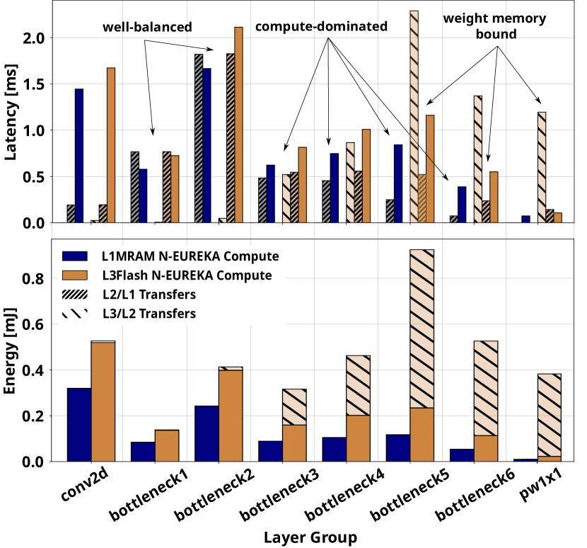
IV-C Layer-wise DNN latency/energy analysis
We further evaluate the impact of MRAM integration by analyzing the effect on each network layer in detail. We focus our analysis on latency and energy in the L1MRAM and L3Flash scenarios, as shown in Figure 10. We use double-buffering on every memory hierarchy level and report the accumulated latency of memory transfer and compute steps during each layer’s execution; as such, the overall latency is determined by the latency of the slowest step. We find three distinct regimes of operation: in the well-balanced regime, found in the first two bottleneck layers, the overall latency is approximately equally distributed between compute and memory access. In the compute-dominated regime, the latency of computations outweighs the latency of memory transfers. The last regime we distinguish is the weight memory bound regime, where latency and energy consumption are dominated by memory transfers for the L3Flash scenario. Figure 10 shows a clear trend; in deeper network layers, where the ratio between spatial dimensions and filter dimensions, and thus weight reuse, is lower, the benefit of a dedicated weight memory subsystem becomes evident. The energy savings in the fifth bottleneck layer are especially notable. By eliminating transfers for weights, we reduce the energy consumption of the layer by 8.
We can trace the performance improvements unlocked by our architecture to three key design considerations in Siracusa. First, coupling the MRAM directly with N-EUREKA allows us to maximize the available bandwidth towards the accelerator. In Siracusa, the weight memory subsystem doubles the available bandwidth of the accelerator in the Cluster domain to . Second, integrating MRAM sized to hold all the weights of the most common DNNs on the chip drastically reduces the energy spent on data movement. While we measure an almost 2 reduction of energy cost for all MRAM-based designs by eliminating off-chip memory transfers, eliminating all on-chip weight transfers further reduces the end-to-end energy per inference by 1.7. Third, by keeping the weights statically in the weight memory subsystem and eliminating weight accesses from the TCDM, additional L1 bandwidth is available for activation data movement. Although we find that eliminating the L3L2 bottleneck decreases latency by 1.15 - 1.36, unlocking extra bandwidth towards the last memory level further increases throughput by an additional 27 %.
V SoA Comparison
Vega[23] DIANA[20] MARSELLUS[4] Chang et al.[25] Zhang et al.[8] THIS WORK Technology 22nm FDX 22nm FDX 22nm FDX 40nm 22nm 16nm FinFET Area Cluster: , IO-Domain: Applications IoT GP+DNN SoC AI-IoT SoC IoT GP+AI-IoT SoC Edge AI ASIC GP+DNN Robot SoC XR SoC Cores 10 RV32IMCFXpulp 1 RV32IMCFXpulp 1 RV32IMCFXpulp 1 1 Cortex-M3 Cortex-M33 1 RV32IMCFXpulp +Convolution Engine +digital NE +16 RV32IMCFXpulpnn +MAC Array +NVPU +8 RV32IMCFXpulpnn +AIMC SRAM +NE +N-EUREKA On-Chip SRAM (L1) (L1) (L1) (L2) (in/out+weights) (L2) + (L2) + (SRAM) On-chip NVM MRAM (L3) - - RRAM (L2) MRAM (L1) INT Precision 8, 16, 32 2, 4, 8, 16, 32 2, 4, 8, 16, 32 (RISC-V) 1, 4, 8 (MAC Array) 16 2, 4, 8, 16, 32 (RISC-V) 2-8 (RBE) 32 (Cortex-M3) 2-8b W, 8b in/out (N-EUREKA) Supply Voltage Max Frequency to Power Range to (digital NE) to Peak Performance (8-bit) (digital NE) N/A (16b in/W) Peak Efficiency (8-bit, no sparsity) (16b in/W, @ 80% W sparsity) Peak Performance (digital NE) N/A (Best) (AIMC-SRAM) (2b in, 2b W) (16b in/W) (8b in, 2b W) Peak Efficiency (digital NE, 2b in/W) (Best, no sparsity) (8b in/W) (AIMC-SRAM) (2b in/W) (1b in/W) (16b in/W, @ 80% W sparsity) (8b in, 2b W) Peak Binary (digital NE, 2b in/W) Equivalent Efficiency (8b in/W) (2b in/W) (1b in/W) (16b in/W) (8b in, 2b W) Peak Area Efficiency (digital NE) (cluster) N/A (cluster)
Emerging near-sensor XR requires combining high performance in crucial AI kernels with flexibility and low power footprint to enable integration in wearable devices. In Table II, we compare Siracusa’s performance and efficiency with that of state-of-the-art computing platforms for near-sensor XR, accelerated extreme-edge AI, and near-sensor computing – using a variety of technologies such as embedded NVM [23, 8], Analog In-Memory Computing (AIMC) [20], and digital acceleration [4, 25, 8]. While Zhang et al. [8] use a non-standard normalization factor of 1 16-bit-MAC = 7 Ops in their paper, we report all results considering 1 MAC = 2 Ops at native precision for fairness. Although there is a rich body of literature to motivate aggressive pruning of neural networks, the impact of sparsity on the energy efficiency of accelerators is mainly dependent on the distribution of zeros; however, accounting for the structure of sparsity in DNN weights is nearly impossible [26]. Therefore, to fairly compare the energy efficiency of different designs, we chose to normalize all reported efficiency numbers to 0 % weight sparsity. To the best of the authors’ knowledge, Siracusa is the first SoC to integrate non-volatile MRAM closely coupled to an all-digital DNN accelerator. Siracusa achieves the best peak performance of (8b activation, 2b weight configuration) compared to other works [23, 4, 25, 8] except DIANA[20] ’s SRAM-based AIMC accelerator. Regarding 8-bit peak performance, it provides the absolute highest performance compared to the other works in Table II, due to the large embedded N-EUREKA engine.
Considering energy efficiency, Siracusa achieves the highest peak efficiency at 8-bit precision compared to all SoCs considered when normalizing for 0 % sparsity. Neglecting this normalization, Zhang et al. [8] report a 31 % higher overall energy efficiency than our work; however, these results are obtained with a very high sparsity rate (80 % for weights, 50 % for activations). Finally, when considering the best overall efficiency (i.e., at any precision), Siracusa achieves with 2-bit weights and 8-bit activations. This compares favorably to other digital SoCs; even when considering instances where the absolute efficiency reported is better, Siracusa is competitive regarding energy per elementary operation. We can highlight this fact by considering equivalent binary operations (Bops)222 Bops = : Siracusa achieves ; Marsellus [4] achieves ; and Chang et al. [25] achieve . The only digital SoC achieving higher binary efficiency than Siracusa is Zhang et al.’s [8] (): in their case, the choice to use 16-bit inputs and weights boosts this particular metric, due to the more accurate numerical representation. The AIMC accelerator in DIANA offers 67 better peak energy efficiency compared to Siracusa; however, exploiting this design to high utilization and full efficiency is very complex according to DIANA’s own architects [27], and this efficiency comes at a steep price in terms of noise and accuracy. At 8-bit precision, Siracusa achieves the highest peak efficiency compared to all considered SoCs.
The embedded MRAM NVM and its tight integration with the accelerator set N-EUREKA apart from all other SoCs of similar class. As discussed in Section IV, a large NVM is necessary to run common edge DNNs fully on-chip, and the L1 tight integration strategy employed in Siracusa maximizes performance gains in end-to-end execution. Of the considered SoCs, only Vega [23] and Siracusa include enough on-chip MRAM to support the execution of a MobileNet-V2 network [24] at 8-bit precision. We observe that as NVMs are typically not symmetric in read and write power and latency, it is not possible to use them as on-chip cache for a larger off-chip weight memory; therefore, the other considered SoCs need to use off-chip transfers to run common edge DNNs, suffering from a heavy penalty on both end-to-end latency and efficiency.
Finally, thanks to the high-density on-chip integration of MRAM near N-EUREKA, Siracusa achieves the best area efficiency compared to the existing SoA architectures[23, 20, 4] – a prerequisite to enabling high-performance and low power in a constrained form factor and overall cost as necessary for XR wearable devices.
VI Conclusion
In this work, we presented three key ideas to integrate emerging MRAM within a state-of-the-art XR near-sensor computing system, and evaluated their impact in terms of energy efficiency and end-to-end latency of realistic DNNs. The key innovations demonstrated in this work are: 1) Closely coupling non-volatile MRAM as dedicated weight memory with the system’s accelerator unlocks additional bandwidth for weight transfers during network inference, doubling the effective bandwidth for layers with low weight reuse. 2) Leveraging the high memory density of MRAM enables all-weights-on-chip inference, drastically reducing the energy cost of data movement for DNN inference and consequently improving end-to-end energy efficiency. 3) Careful design of the accelerator’s weight memory access pattern and integration of a low-overhead MRAM pipelining system allows us to prefetch network weights in a non-speculative manner, fully compensating for the slower-than-SRAM read access time of MRAM without impacting energy efficiency.
The combined effect of these key innovations improves the end-to-end inference latency of DNN workloads by 1.7 and reduces their energy cost by 4.1 compared to conventional systems using off-chip NVM. While pure AIMC macros achieve higher peak efficiency than our all-digital accelerator, we demonstrate end-to-end deployment results of realistic DNN workloads, achieving a throughput of on 8-bit quantized networks, 4.8 more than the highest value reported in XR SoC literature, while achieving state-of-the-art energy efficiency of . Thanks to the tight integration of high-density MRAM with N-EUREKA, Siracusa’s Cluster improves on the state-of-the-art in compute area efficiency by 10 % while integrating of memory, 1.8 more than Vega [23], the design with the largest amount of on-chip memory.
References
- [1] M. Abrash, “Creating the Future: Augmented Reality, the next Human-Machine Interface,” in 2021 IEEE International Electron Devices Meeting (IEDM). San Francisco, CA, USA: IEEE, Dec. 2021, pp. 1–11. [Online]. Available: https://ieeexplore.ieee.org/document/9720526/
- [2] S. Han, B. Liu, R. Cabezas, C. D. Twigg, P. Zhang, J. Petkau, T.-H. Yu, C.-J. Tai, M. Akbay, Z. Wang, A. Nitzan, G. Dong, Y. Ye, L. Tao, C. Wan, and R. Wang, “MEgATrack: monochrome egocentric articulated hand-tracking for virtual reality,” ACM Transactions on Graphics, vol. 39, no. 4, Aug. 2020. [Online]. Available: https://dl.acm.org/doi/10.1145/3386569.3392452
- [3] Y. Feng, N. Goulding-Hotta, A. Khan, H. Reyserhove, and Y. Zhu, “Real-Time Gaze Tracking with Event-Driven Eye Segmentation,” in 2022 IEEE Conference on Virtual Reality and 3D User Interfaces (VR). Christchurch, New Zealand: IEEE, Mar. 2022, pp. 399–408. [Online]. Available: https://ieeexplore.ieee.org/document/9756796/
- [4] F. Conti, G. Paulin, A. Garofalo, D. Rossi, A. D. Mauro, G. Rutishauser, G. Ottavi, M. Eggimann, H. Okuhara, and L. Benini, “Marsellus: A Heterogeneous RISC-V AI-IoT End-Node SoC With 2–8 b DNN Acceleration and 30%-Boost Adaptive Body Biasing,” IEEE Journal of Solid-State Circuits, pp. 1–15, 2023, conference Name: IEEE Journal of Solid-State Circuits. [Online]. Available: https://ieeexplore.ieee.org/document/10269153
- [5] A. Di Mauro, M. Scherer, D. Rossi, and L. Benini, “Kraken: A Direct Event/Frame-Based Multi-sensor Fusion SoC for Ultra-Efficient Visual Processing in Nano-UAVs,” in 2022 IEEE Hot Chips 34 Symposium (HCS). Cupertino, CA, USA: IEEE, Aug. 2022, pp. 1–19. [Online]. Available: https://ieeexplore.ieee.org/document/9895621/
- [6] I. Miro-Panades, B. Tain, J.-F. Christmann, D. Coriat, R. Lemaire, C. Jany, B. Martineau, F. Chaix, G. Waltener, E. Pluchart, J.-P. Noel, A. Makosiej, M. Montoya, S. Bacles-Min, D. Briand, J.-M. Philippe, Y. Thonnart, A. Valentian, F. Heitzmann, and F. Clermidy, “SamurAI: A Versatile IoT Node With Event-Driven Wake-Up and Embedded ML Acceleration,” IEEE Journal of Solid-State Circuits, vol. 58, no. 6, pp. 1782–1797, Jun. 2023. [Online]. Available: https://ieeexplore.ieee.org/document/9874917/
- [7] L. Yang, R. M. Radway, Y.-H. Chen, T. F. Wu, H. Liu, E. Ansari, V. Chandra, S. Mitra, and E. Beigné, “Three-Dimensional Stacked Neural Network Accelerator Architectures for AR/VR Applications,” IEEE Micro, vol. 42, no. 6, pp. 116–124, Nov. 2022, conference Name: IEEE Micro. [Online]. Available: https://ieeexplore.ieee.org/document/9933882
- [8] Q. Zhang, H. An, Z. Fan, Z. Wang, Z. Li, G. Wang, H.-S. Kim, D. Blaauw, and D. Sylvester, “A 22nm 3.5TOPS/W Flexible Micro-Robotic Vision SoC with 2MB eMRAM for Fully-on-Chip Intelligence,” in 2022 IEEE Symposium on VLSI Technology and Circuits (VLSI Technology and Circuits), Jun. 2022, pp. 72–73, iSSN: 2158-9682. [Online]. Available: https://ieeexplore.ieee.org/abstract/document/9830340
- [9] Y.-C. Chiu, W.-S. Khwa, C.-Y. Li, F.-L. Hsieh, Y.-A. Chien, G.-Y. Lin, P.-J. Chen, T.-H. Pan, D.-Q. You, F.-Y. Chen, A. Lee, C.-C. Lo, R.-S. Liu, C.-C. Hsieh, K.-T. Tang, Y.-D. Chih, T.-Y. Chang, and M.-F. Chang, “A 22nm 8Mb STT-MRAM Near-Memory-Computing Macro with 8b-Precision and 46.4-160.1TOPS/W for Edge-AI Devices,” in 2023 IEEE International Solid- State Circuits Conference (ISSCC). San Francisco, CA, USA: IEEE, Feb. 2023, pp. 496–498. [Online]. Available: https://ieeexplore.ieee.org/document/10067563/
- [10] P.-H. Lee, C.-F. Lee, Y.-C. Shih, H.-J. Lin, Y.-A. Chang, C.-H. Lu, Y.-L. Chen, C.-P. Lo, C.-C. Chen, C.-H. Kuo, T.-L. Chou, C.-Y. Wang, J. J. Wu, R. Wang, H. Chuang, Y. Wang, Y.-D. Chih, and T.-Y. J. Chang, “33.1 A 16nm 32Mb Embedded STT-MRAM with a 6ns Read-Access Time, a 1M-Cycle Write Endurance, 20-Year Retention at 150°C and MTJ-OTP Solutions for Magnetic Immunity,” in 2023 IEEE International Solid- State Circuits Conference (ISSCC). San Francisco, CA, USA: IEEE, Feb. 2023, pp. 494–496. [Online]. Available: https://ieeexplore.ieee.org/document/10067837/
- [11] M. Scherer, M. Eggimann, A. D. Mauro, A. S. Prasad, F. Conti, D. Rossi, J. T. Gómez, Z. Li, S. S. Sarwar, Z. Wang, B. D. Salvo, and L. Benini, “Siracusa: A Low-Power On-Sensor RISC-V SoC for Extended Reality Visual Processing in 16nm CMOS,” in ESSCIRC 2023- IEEE 49th European Solid State Circuits Conference (ESSCIRC). Lisbon, Portugal: IEEE, Sep. 2023, pp. 217–220. [Online]. Available: https://ieeexplore.ieee.org/document/10268718/
- [12] H. Murakami, E. Bohannon, J. Childs, G. Gui, E. Moule, K. Hanzawa, T. Koda, C. Takano, T. Shimizu, Y. Takizawa, A. Basavalingappa, R. Childs, C. Cziesler, R. Jarnot, K. Nishimura, S. Rogerson, and Y. Nitta, “A 4.9Mpixel Programmable-Resolution Multi-Purpose CMOS Image Sensor for Computer Vision,” in 2022 IEEE International Solid- State Circuits Conference (ISSCC). San Francisco, CA, USA: IEEE, Feb. 2022, pp. 104–106. [Online]. Available: https://ieeexplore.ieee.org/document/9731607/
- [13] F. Montagna, S. Mach, S. Benatti, A. Garofalo, G. Ottavi, L. Benini, D. Rossi, and G. Tagliavini, “A Low-Power Transprecision Floating-Point Cluster for Efficient Near-Sensor Data Analytics,” IEEE Transactions on Parallel and Distributed Systems, vol. 33, no. 5, pp. 1038–1053, May 2022. [Online]. Available: https://ieeexplore.ieee.org/document/9506919/
- [14] C. Jie, I. Loi, L. Benini, and D. Rossi, “Energy-Efficient Two-level Instruction Cache Design for an Ultra-Low-Power Multi-core Cluster,” in 2020 Design, Automation & Test in Europe Conference & Exhibition (DATE). Grenoble, France: IEEE, Mar. 2020, pp. 1734–1739. [Online]. Available: https://ieeexplore.ieee.org/document/9116212/
- [15] A. Prasad, L. Benini, and F. Conti, “Specialization meets Flexibility: a Heterogeneous Architecture for High-Efficiency, High-flexibility AR/VR Processing,” in Proceedings of the 2023 Design Automation Conference (DAC 2023), to appear, 2023.
- [16] M. Rusci and T. Tuytelaars, “On-Device Customization of Tiny Deep Learning Models for Keyword Spotting With Few Examples,” IEEE Micro, vol. 43, no. 6, pp. 50–57, Nov. 2023, conference Name: IEEE Micro. [Online]. Available: https://ieeexplore.ieee.org/abstract/document/10241972
- [17] F. Conti, “Technical Report: NEMO DNN Quantization for Deployment Model,” Apr. 2020, arXiv:2004.05930 [cs, stat]. [Online]. Available: http://arxiv.org/abs/2004.05930
- [18] S. Ikegawa, F. B. Mancoff, J. Janesky, and S. Aggarwal, “Magnetoresistive Random Access Memory: Present and Future,” IEEE Transactions on Electron Devices, vol. 67, no. 4, pp. 1407–1419, Apr. 2020. [Online]. Available: https://ieeexplore.ieee.org/document/8976130/
- [19] Z. Guo, J. Yin, Y. Bai, D. Zhu, K. Shi, G. Wang, K. Cao, and W. Zhao, “Spintronics for Energy- Efficient Computing: An Overview and Outlook,” Proceedings of the IEEE, vol. 109, no. 8, pp. 1398–1417, Aug. 2021, conference Name: Proceedings of the IEEE. [Online]. Available: https://ieeexplore.ieee.org/abstract/document/9452065
- [20] P. Houshmand, G. M. Sarda, V. Jain, K. Ueyoshi, I. A. Papistas, M. Shi, Q. Zheng, D. Bhattacharjee, A. Mallik, P. Debacker, D. Verkest, and M. Verhelst, “DIANA: An End-to-End Hybrid DIgital and ANAlog Neural Network SoC for the Edge,” IEEE Journal of Solid-State Circuits, vol. 58, no. 1, pp. 203–215, Jan. 2023. [Online]. Available: https://ieeexplore.ieee.org/document/9932871/
- [21] S. Angizi, Z. He, A. Awad, and D. Fan, “MRIMA: An MRAM-Based In-Memory Accelerator,” IEEE Transactions on Computer-Aided Design of Integrated Circuits and Systems, vol. 39, no. 5, pp. 1123–1136, May 2020, conference Name: IEEE Transactions on Computer-Aided Design of Integrated Circuits and Systems. [Online]. Available: https://ieeexplore.ieee.org/abstract/document/8675492
- [22] W. Kang, H. Wang, Z. Wang, Y. Zhang, and W. Zhao, “In-Memory Processing Paradigm for Bitwise Logic Operations in STT–MRAM,” IEEE Transactions on Magnetics, vol. 53, no. 11, pp. 1–4, Nov. 2017, conference Name: IEEE Transactions on Magnetics. [Online]. Available: https://ieeexplore.ieee.org/abstract/document/7927489
- [23] D. Rossi, F. Conti, M. Eggiman, A. D. Mauro, G. Tagliavini, S. Mach, M. Guermandi, A. Pullini, I. Loi, J. Chen, E. Flamand, and L. Benini, “Vega: A Ten-Core SoC for IoT Endnodes With DNN Acceleration and Cognitive Wake-Up From MRAM-Based State-Retentive Sleep Mode,” IEEE Journal of Solid-State Circuits, vol. 57, no. 1, pp. 127–139, Jan. 2022, conference Name: IEEE Journal of Solid-State Circuits.
- [24] M. Sandler, A. Howard, M. Zhu, A. Zhmoginov, and L.-C. Chen, “MobileNetV2: Inverted Residuals and Linear Bottlenecks,” 2018. [Online]. Available: https://arxiv.org/abs/1801.04381
- [25] M. Chang, S. D. Spetalnick, B. Crafton, W.-S. Khwa, Y.-D. Chih, M.-F. Chang, and A. Raychowdhury, “A 40nm 60.64TOPS/W ECC-Capable Compute-in-Memory/Digital 2.25MB/768KB RRAM/SRAM System with Embedded Cortex M3 Microprocessor for Edge Recommendation Systems,” in 2022 IEEE International Solid- State Circuits Conference (ISSCC). San Francisco, CA, USA: IEEE, Feb. 2022, pp. 1–3. [Online]. Available: https://ieeexplore.ieee.org/document/9731679/
- [26] T. Hoefler, D. Alistarh, T. Ben-Nun, and N. Dryden, “Sparsity in deep learning,” The Journal of Machine Learning Research, vol. 22, no. 1, pp. 1–124, Jan. 2021.
- [27] J. Van Delm, M. Vandersteegen, A. Burrello, G. M. Sarda, F. Conti, D. J. Pagliari, L. Benini, and M. Verhelst, “HTVM: Efficient Neural Network Deployment On Heterogeneous TinyML Platforms,” in 2023 60th ACM/IEEE Design Automation Conference (DAC). San Francisco, CA, USA: IEEE, Jul. 2023, pp. 1–6. [Online]. Available: https://ieeexplore.ieee.org/document/10247664/