The development of bias current source for time-division superconducting quantum interference device multiplexer
Abstract
Transition-edge sensors (TESs) are useful devices for detecting photons from sub-millimeter radiation to rays, which is typically operate at a current bias point. The problem of large-scale array applications of TES is the low-temperature multiplexed readout based on superconducting quantum interference device (SQUID). The most mature technology currently is the time-division multiplexing SQUID (TDM). To provide TDM with appropriate current bias, we design a Configurable Ultra-Low Noise Current Source (CLCS), which is based on the feedback structure of ultra-low noise instrumentation amplifiers and low-noise, high-resolution (20 bits) digital-to-analog converter (DAC). The high-impedance output of the CLCS avoids the issue of impedance mismatch. CLCS has an ultra-high resolution of in the to current output range. To test the performance of the CLCS, we use three TESs, which have different structure, to conduct I-V testing, and then compare the results with the commercial power supply module SIM928. On the other hand, we compare the output noise level of CLCS with SIM928, and analyze the total system noise at different current bias of TES. All the above measurement and analysis validate that the performance of CLCS meets the experimental requirements.
1 Introduction
Transition-edge sensors (TESs) are useful superconducting devices for detecting photons from sub-millimeter radiation to rays. TES generally works at specific current bias point. The schematic diagram of TES is shown in figure 1.
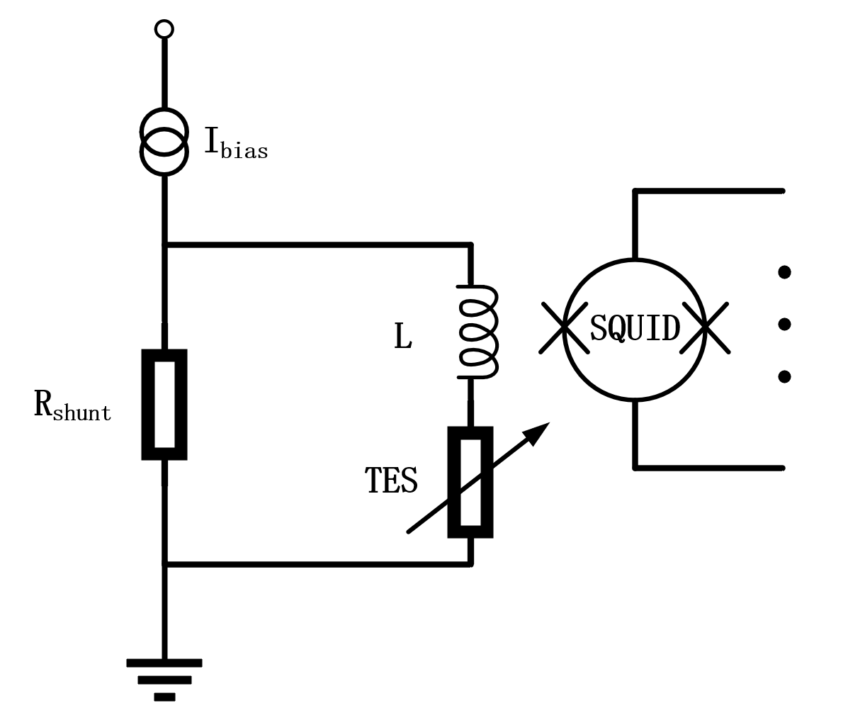
TES is connected in series with a inductive coil , and in parallel with a shunt resistor , which couples TES output signal to the superconducting quantum interference device (SQUID) readout system. TES requires an external bias current to operate [1, 2, 3, 4, 5]. The problem of large-scale array applications of TES is the low-temperature multiplexed readout based on SQUID. The most mature technology currently is the time-division multiplexing SQUID (TDM) readout electronics. TDM electronics are used on many experiments, like SCUBA-2 [6, 7], ACT [8], Spider [9, 10], BICEPII [10] and SPUD [10]. The multi-stage SQUID readout architecture of TDM achieves multiplexed readout of multiple detectors by cyclically selecting each row’s first-stage SQUID, which greatly reduces power consumption at each stage for the system. In addition to TES, each SQUID stage needs low noise bias source. SQUID is same low noise device as TES [11, 12, 13, 14, 15, 16]. The TDM multiplexing architecture and bias source distribution are shown in figure 2.
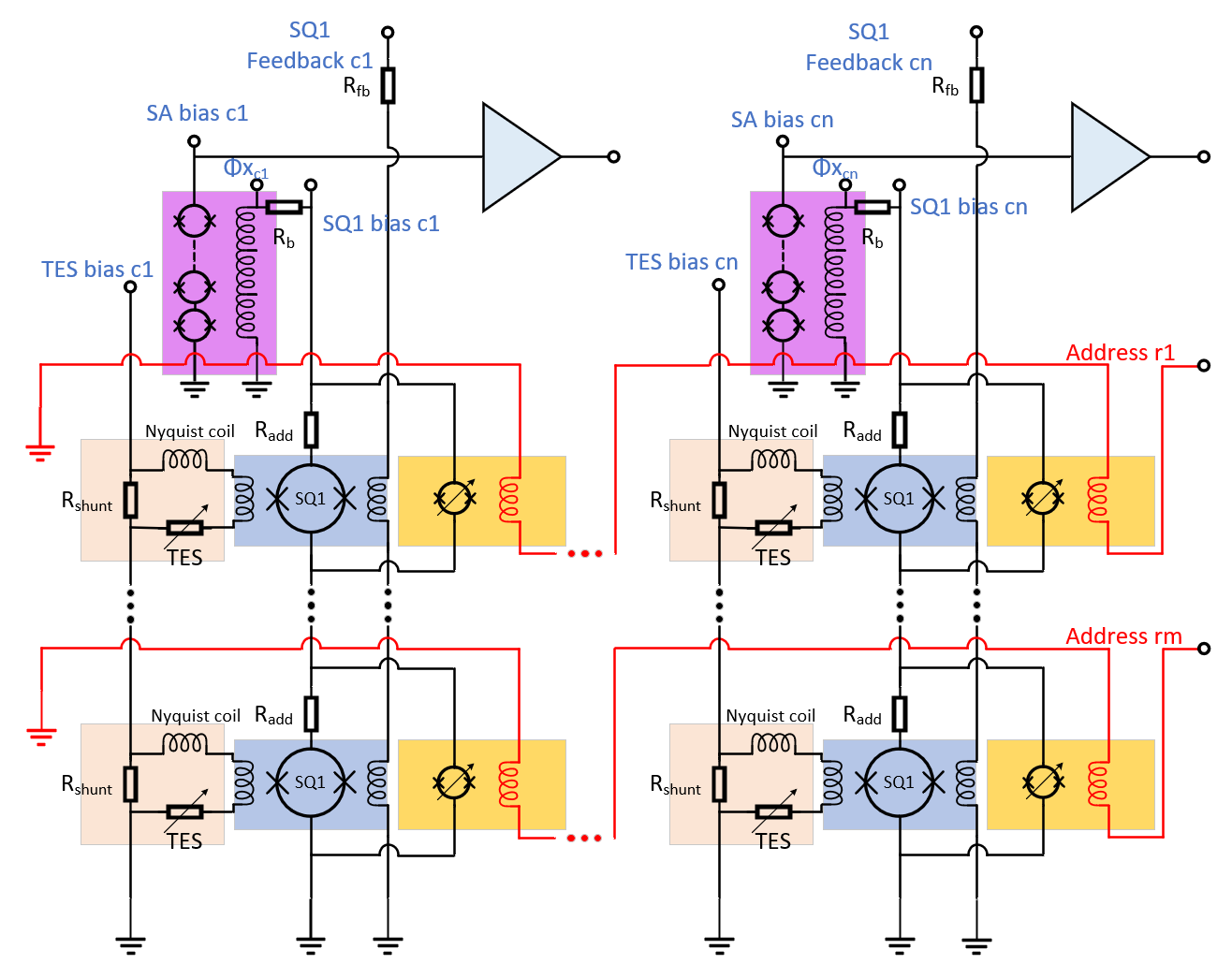
The figure shows an multiplexed array structure. Each column of multiplexed TES and SQUID requires a low-noise bias source. We design a Configurable Ultra-Low Noise Current Source (CLCS) as a bias source device for TDM, and test the performance of CLCS based on TES in this paper.
The way to know which bias is suitable for TES is by analyzing current-voltage (I-V) curve. We can also get the critical temperature , the critical current , the normal resistance , the thermal conductance between the TES and the heat sink, and the thermal conducting index from I-V feature. It is important to provide the TES with the appropriate bias current. The common way is using a ultra-low noise voltage source, like SRS SIM928 (with digital-to-analog converter, DAC AD5541, 16 bits), in series with a large resistor to convert voltage into an approximate current. The bias source electronics (DAC MAX5443, 16 bits) designed by NIST and UBC’s Multi-Channel Electronics (MCE) also follow this approach [11, 17]. We have found that although the impedance of TES is very small, the impedance across the entire bias circuit is around several tens of ohms in the laboratory. Even if we use enough large resistor to do voltage-current transfer, the resistance of bias circuit is non-negligible. This is because TES is particularly sensitive to current changes in the superconducting transition region. A little change of resistance will influence the bias state of TES. On the other hand, the digital resolution of most of the commercial low-noise programmable power source typically does not exceed 16 bits. To improve the current output resolution is crucial for the operation of TES.
The paper is organized as follows: section 2 presents the design principles of CLCS and testing system, section 3 presents the thermal and electrical parameters of TES through I-V curve analysis and compares the basic functional performance of the commercial source module SIM928 with CLCS, section 4 compares the noise levels of SIM928 and CLCS, and further compares their noise contributions by analyzing the overall noise of the system in which TES is located, section 5 simply presents the alternating current (AC) waveform functions, and section 6 concludes the paper.
2 System design
2.1 Bias source electronics
The core of the bias module is to select precision instrument amplifiers with differential symmetric structure and low-noise, high-precision digital-to-analog converter (DAC). The operational amplifiers have high-input and low-output impedance. To achieve constant current output and adjustable current output, we can utilize a simple feedback structure [18, 19, 20]. The design principle of the entire CLCS module is shown on the left side of figure 3.
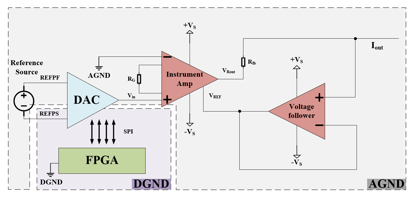
To ensure high-precision regulation of current output and to enhance the driving capability of the DAC, the input of the instrumentation amplifier is connected to the output of the DAC module. The DAC module is DAC11001B of TI, which has 20-bit high-resolution single-channel configurable output based on the Serial Peripheral Interface (SPI) protocol. It also has low output noise, approximately as stated in the datasheet. The pin of DAC11001B determines the output voltage range, which is set to to according to the experimental requirements. We use INA849 of TI as the instrumentation amplifier part of CLCS. Its front-end high-impedance input operational amplifier serves as a voltage follower for the DAC. The internal topology ensures that the load and power supply share a common ground, and system stability.
By connecting the feedback resistor to the output terminal of INA849 and using a voltage-follower, it is ensured that there is a fixed voltage difference across the two terminals of . When is chosen appropriately, for example, , an accurate output current on the order of can be obtained. Taking into account the high input impedance of the operational amplifier, the output current can be approximately analyzed, and it can be represented as follows:
| (2.1) | ||||
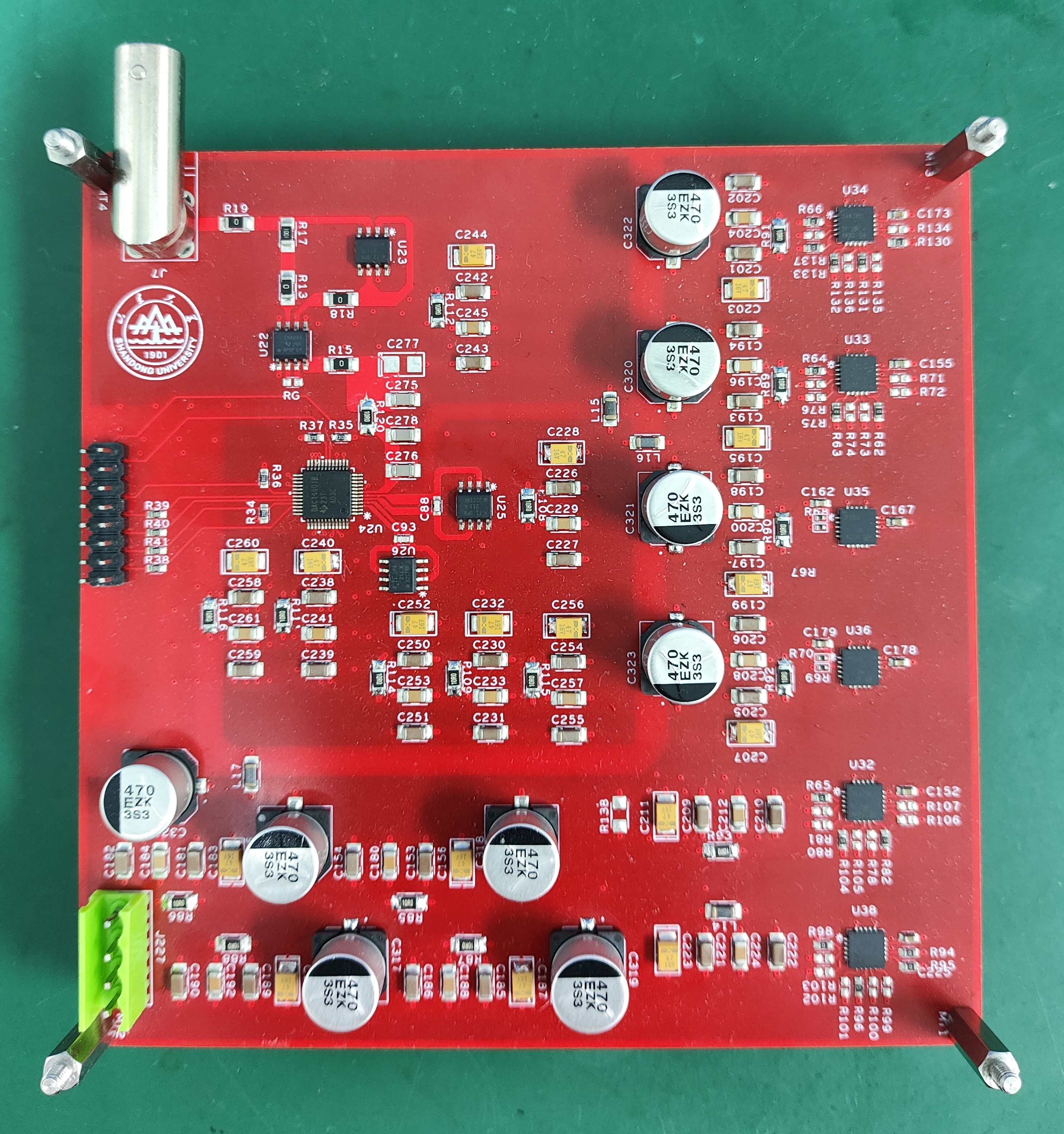
The output voltage of the instrumentation amplifier depends on the power supply limits of the device (). In order to increase the output range, we set as . is the feedback resistor to ensure constant current output, and its resistance value can be adjusted according to the requirements. Here it is set to . is the reference input voltage of the instrumentation amplifier. Due to the resistor outside the pin being in series with the internal resistor of the instrumentation amplifier, this can disrupt the symmetry of the differential amplifier, thereby reducing the common-mode rejection ratio (CMRR). Therefore, a low-noise, low-output impedance operational amplifier is used as the input for the pin. Here we use the TI’s low-noise operational amplifier, OPA211. We connect the output port of OPA211 to its negative input port, and connect positive input to , forming a voltage follower, as figure 3 shows. The high input impedance of the operational amplifier enables that there is a fixed voltage difference across , which is independent of the load, thus providing a constant current. The measured input impedance of the entire system from room temperature end to the cryogenic end, where the TES is located, is approximately . Therefore, the current flowing through , , is almost equal to the current flowing through the load, thus achieving impedance matching. is the input voltage of INA849, and in this single-ended design, its value is equal to the output voltage of the DAC. is the gain factor of the INA849, set to 1 in this case. The physical design of CLCS is shown in figure 3.
The value of will affect the current source resolution and output range. The larger the resistance value, the higher the resolution of the current source, but the corresponding output current range will be smaller. According to the testing requirements of the TES, the output current range of CLCS is configured to be 0 to , with a resolution of up to , which exceeds the capabilities of the SIM928. Refer to table 1 for details.
| to | to | |
2.2 Digital control electronics
To make the configuration of CLCS flexible and convenient for functional design, we will use a Field Programmable Gate Array (FPGA) for digital control of CLCS. We have chosen the Xilinx ARTIX-7 series XC7A35T and will utilize its abundant general purpose input and output (GPIO) resources. Based on the SPI serial protocol, we design interactive logic for the firmware used to configure and monitor the status of CLCS. We use joint test action group (JTAG) interface and small form-factor pluggable (SFP) gigabit optical module to enable information exchange between the FPGA and the host computer, and thus design the corresponding host computer software.
2.3 Testing system
In order to validate the functionality of CLCS, we have set up a testing system that allows for comparison with SIM928. The entire testing system is shown in figure 4.
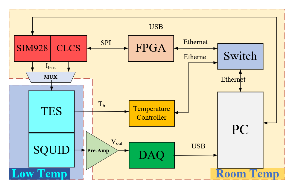
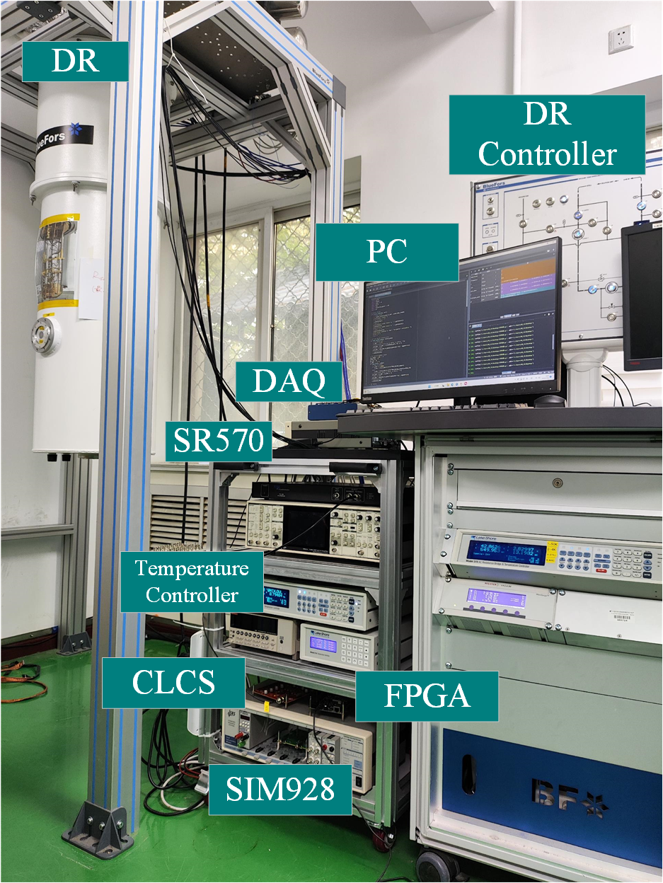
The system utilizes a dilution refrigerator (DR) to operate the TES in the to temperature range. The output of the TES is connected to a low-noise two-stage direct current (DC) SQUID amplifier, to achieve low-noise amplification at the low-temperature end. At room temperature, the signal is connected to a preamplifier for multistage amplification, and the amplified signal is then stored using a data acquisition system (DAQ). The DAQ system is the NI USB-6366, which is equipped with a sampling rate , 16-bit resolution, and 8 channels analog-to-digital converter (ADC). The Lakeshore 372 temperature controller is used to monitor the real-time temperature changes of the TES thermal sink. The FPGA controls and monitors the CLCS output with different bias currents based on the SPI 4-wire protocol. The SIM928 communicates directly with the host computer and is controlled by the host computer. The communication software framework between these devices and the host computer is implemented using the Python libraries socket, pyvisa, and nidaqmx. It is based on the TCP/IP protocol or USB serial communication.
3 I-V feature analysis
We can observe and compare the TES response at different bias point directly from the I-V curve. Based on three TESs of different sizes, the functional response of the SIM928 and CLCS can be compared to verify the basic functionality of the CLCS. Additionally, an analysis can be conducted to assess the impact of different structure sizes on the performance parameters of the TES, under the same doping concentration, thickness, and baking temperature processes. This can help determine whether the performance of the TES meets the design expectations. The structure and distribution of the TES devices used for testing are shown in figure 5.
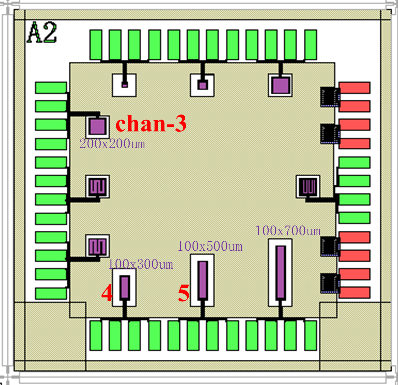
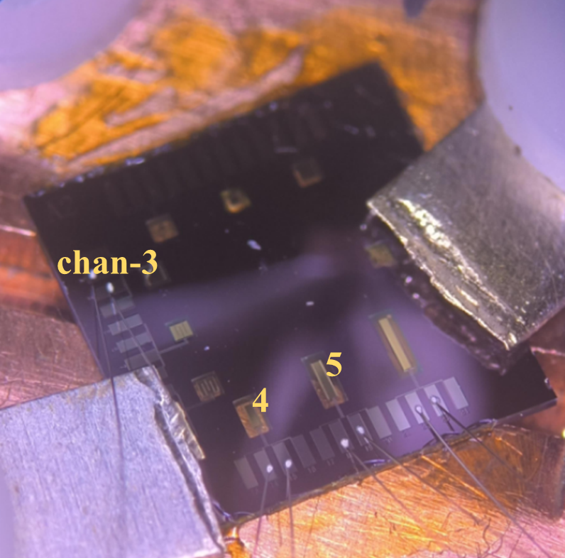
By issuing commands through the Ethernet port (SIM928 is controlled via USB), the CLCS or SIM928 can output specific bias current. Simultaneously, the DAQ card and the temperature controller are synchronized to collect the SQUID output signal and temperature data. After each data acquisition, the system will automatically control the bias power supply to output the next bias current value, and repeat the above operation until the entire testing process is completed. The TES chips we are testing are theoretically designed to have a superconducting transition temperature of approximately , with an ideal operating temperature range of around . We conduct tests on the three different-sized TES at intervals of within the range of to . In order to ensure that the TES can fully transition to the normal state during testing, the bias current range is set to to . The SIM928 achieves the current source circuit equivalently by serially connecting a resistor. As described in section 1 and section 2.1, it is crucial to consider impedance matching when using a voltage source. The high-impedance output of a current source can effectively address impedance matching issues, which is also an important advantage of the CLCS. The I-V test results are shown in figure 6.
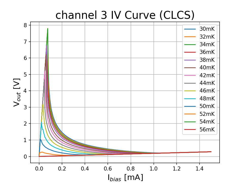
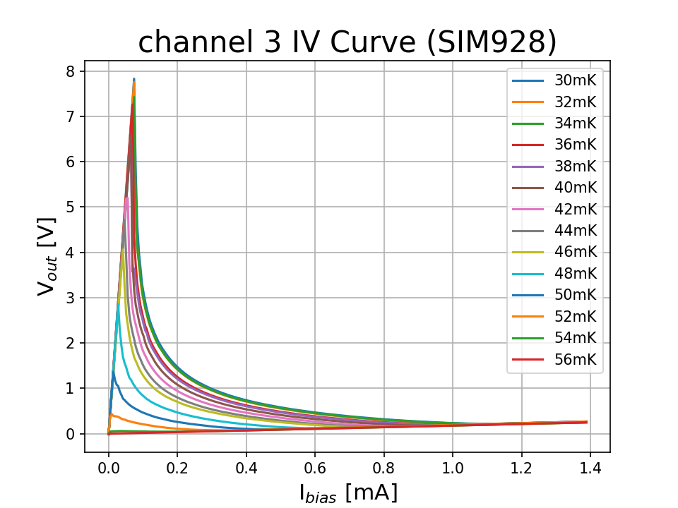
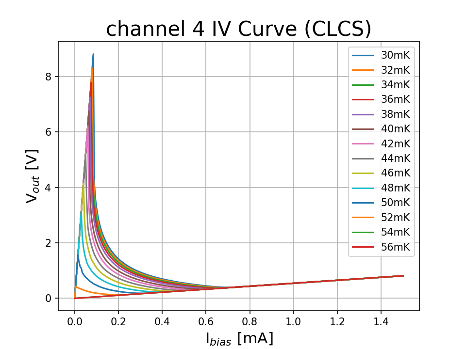
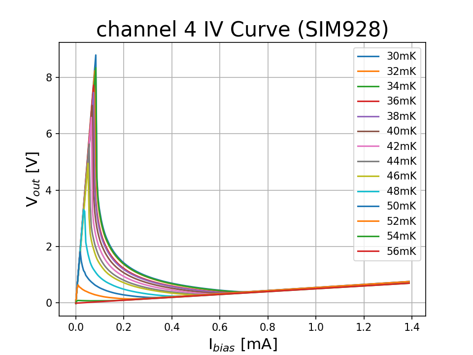
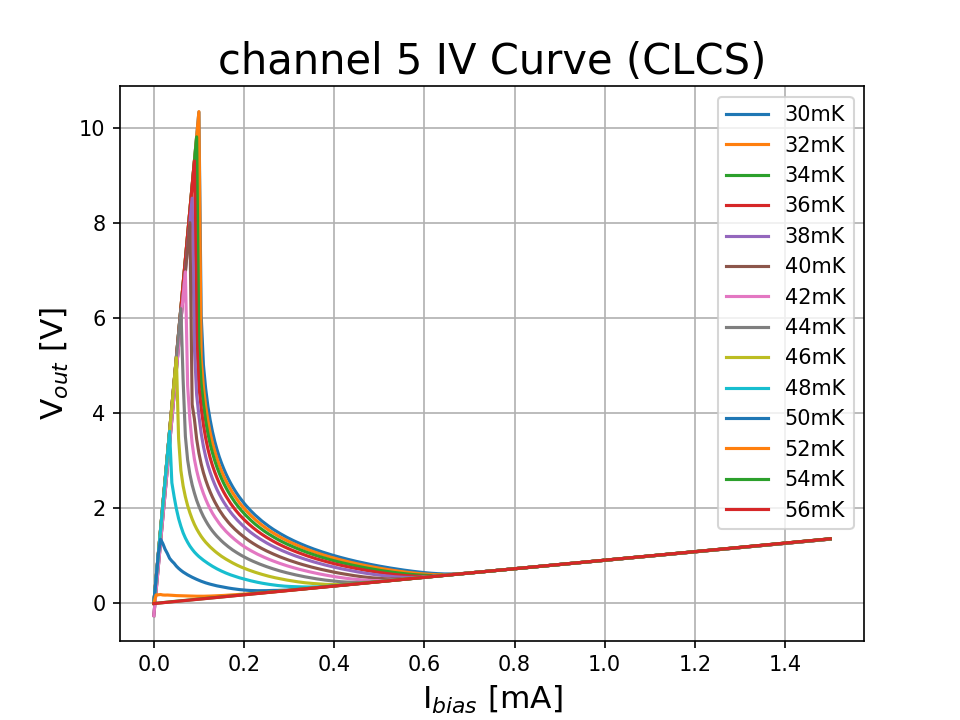
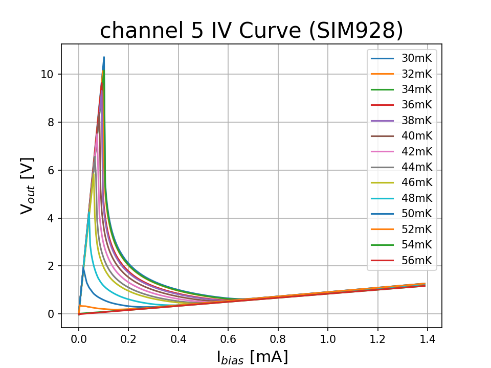
By comparing the results, the I-V curves obtained from testing with CLCS are consistent with the results obtained from testing with SIM928, which effectively validates the basic functionality of CLCS. The feedback coil’s mutual inductance coefficient of SQUID is , where is the flux quantum. The feedback resistor is . Thus, the expected gain should be . Based on the test results at temperature, we can fit the SQUID gain and the normal state resistance () of the TES. The detailed fitting parameters are provided in table 2.
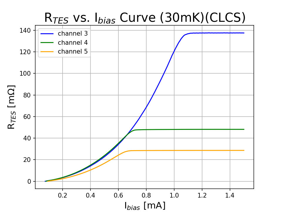
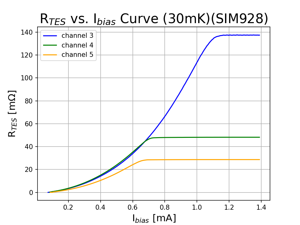
Both the gain and differ by no more than . The ratio of for the three different-sized TES is , which aligns perfectly with the expected design. Further analysis at this temperature can provide the relationship between the bias point and the resistance value of the TES, as shown in figure 7. Detailed results can be found in table 3, which can be further used for noise testing as detailed in section 4.2.
The saturation power () refers to the power level needed to drive the TES into its normal conducting state. It represents the maximum power that the TES can handle without becoming saturated. The value is crucial as it determines the loading conditions under which the detector can effectively operate. By operating the TES below its saturation power, the detector can maintain its sensitivity and linearity for accurate measurements[1, 2, 21]. We define the as the bias power at of the normal resistance (). The of the TES is related to the transition temperature () and thermal conductance () via the following power law
| (3.1) |
where . By analyzing the saturation power, the design of TES can be calibrated. The test results for the 3 TES are shown in figure 8 and table 4.
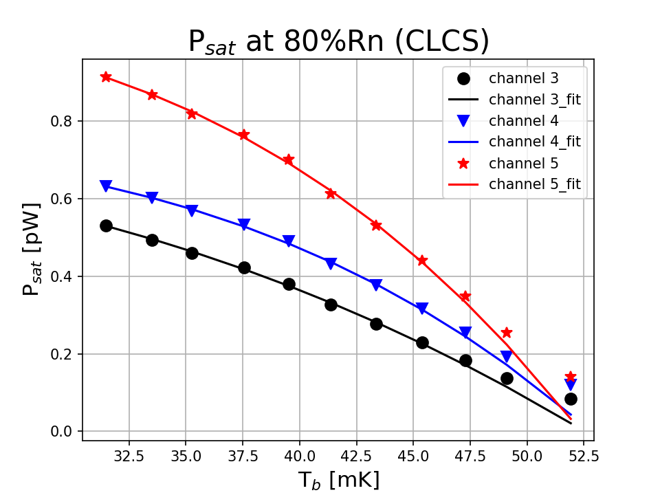
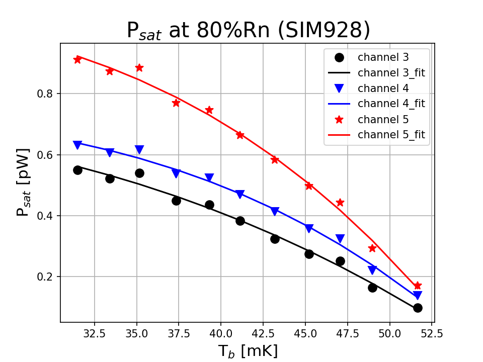
The fitting results show that the differences in , , and are all within , which is in line with the experimental expectations. These results further demonstrate the consistency in functionality between CLCS and SIM928.
4 Noise analysis
Noise is an important factor that must be considered when TES is in operation. The system noise level directly affects the TES resolution. Section 4.1 presents a direct comparison test of the noise power spectral density results of SIM928 and CLCS, using a current amplifier. Section 4.2 analyzes the impact of SIM928 and CLCS on TES by testing the noise performance under different bias current.
4.1 Noise of bias source
We first conducted a comparative test of the intrinsic noise of the two bias source. SIM928 achieves the effect of a current source by connecting a resistor in series. Using Stanford’s low-noise current amplifier, SRS SR570, the current signal is directly amplified and converted into a voltage signal for testing, as shown in figure 9.
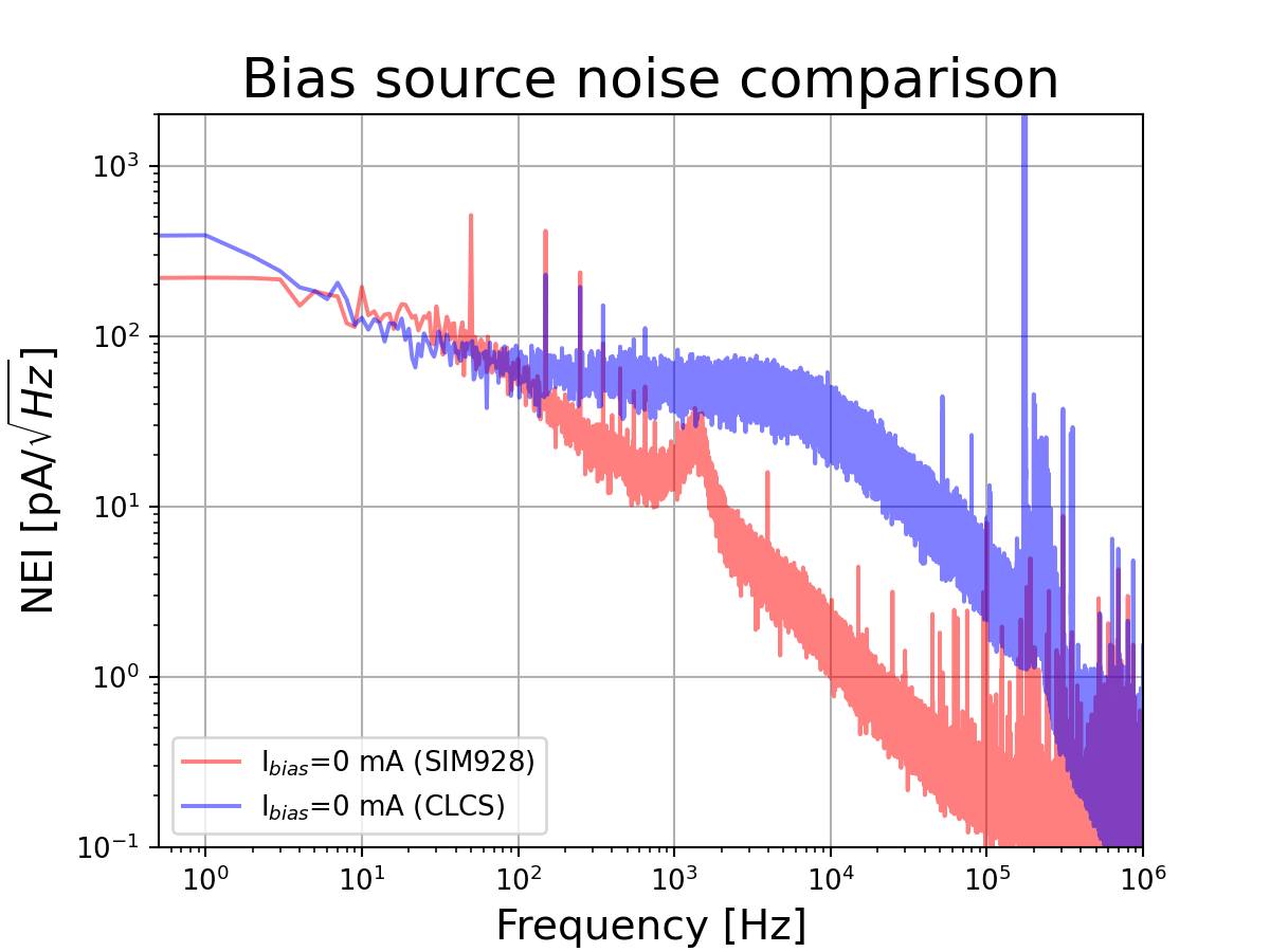
The noise level of CLCS is similar to SIM928 below frequencies. But CLCS has a higher cutoff frequency, which is not the crucial noise component for TES system (see section 4.2 for details).
4.2 Noise of TES system
In order to detect signals, it is common to select an appropriate bias current to place the TES in the superconducting transition region, where it is sensitive to changes in current, as shown in figure 7. In this region, the higher the bias current, the higher the temperature of the TES, which leads to an increase in the resistance of the TES. Because the TES and the shunt resistor are connected in parallel (as shown in figure 1), the current through TES will decrease, resulting in a reduction in noise. By supplying different bias currents, we test TES at , , , and of the normal state resistance (). The noise of the TES system under different biases is shown in figure 10.
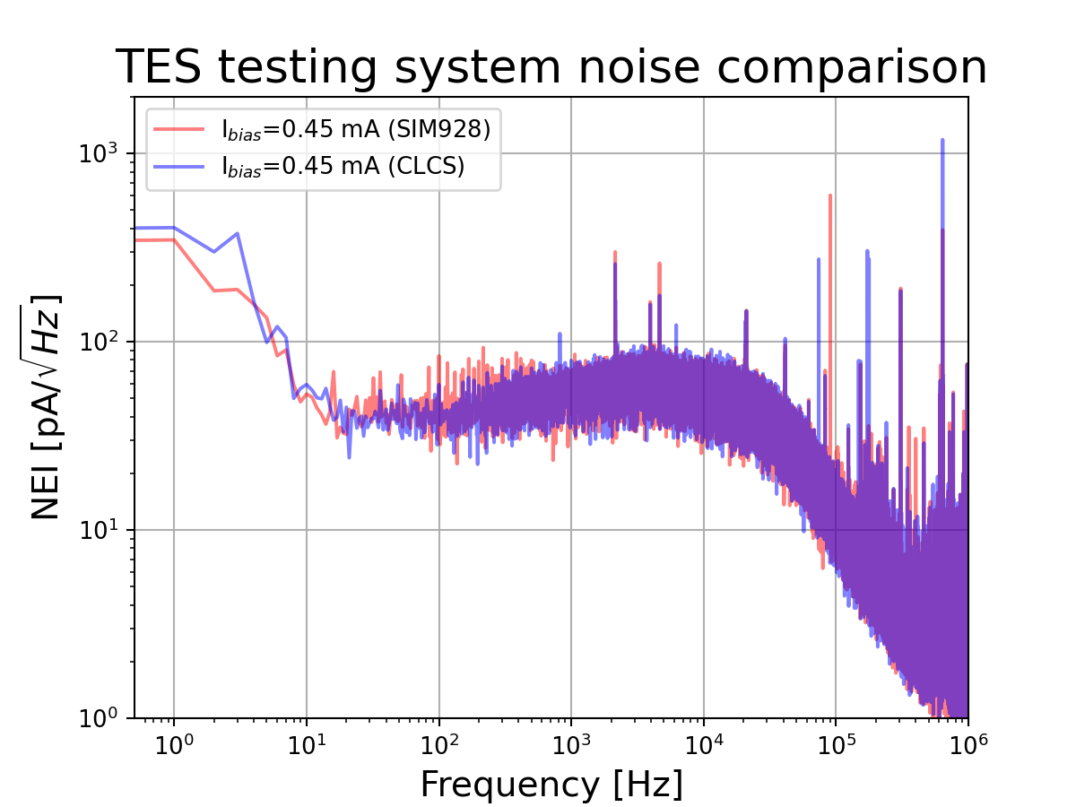
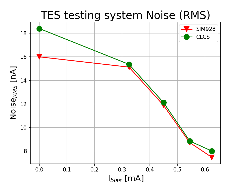
The figure 10 only shows the system noise of one TES. Compared to figure 9, the left figure of 10 shows that both CLCS and SIM928 contribute relatively little to the overall system noise, and their main contributions are in the low-frequency components. The right figure of 10 shows the root mean square (RMS) values at different bias point. We find that RMS value is decrease as the bias current increase, which is in line with the parallel shunt structure of the TES, as shown in figure 1.
5 AC function
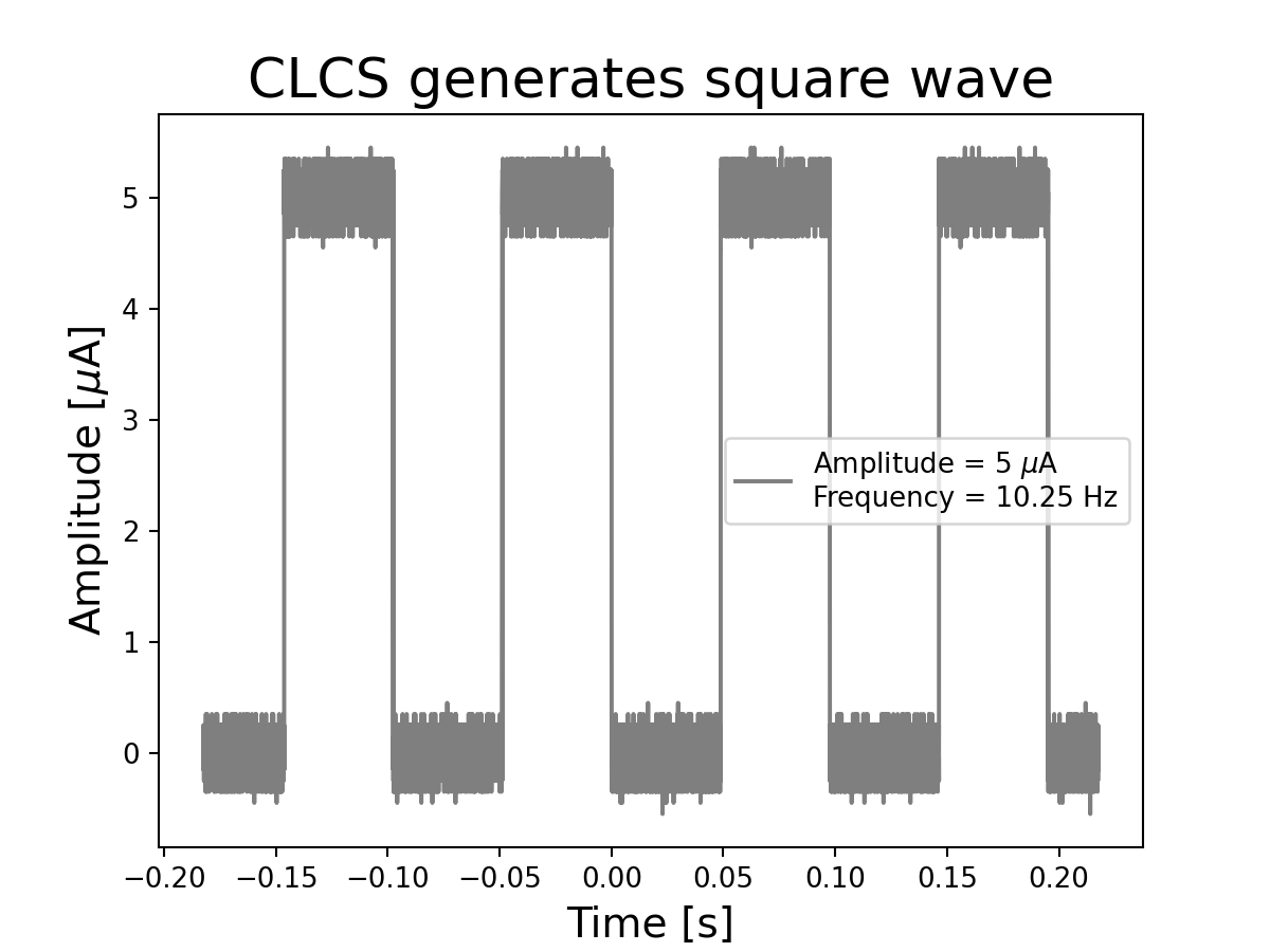
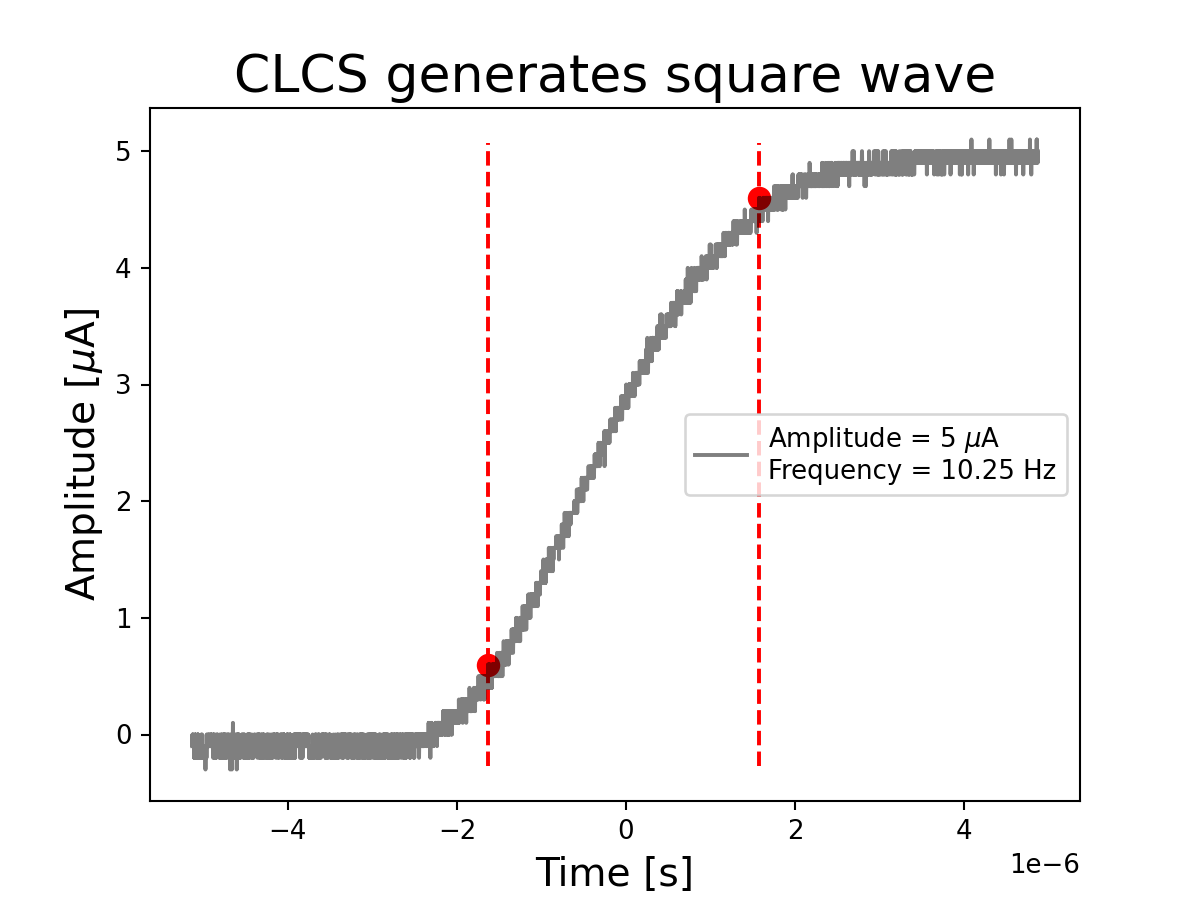
TES need to consider the pulse decay time when receiving signal. For CMB, the time constant is about ms. The general way is using low frequency and small amplitude square wave to test time response of TES. We use CLCS to generate a square wave, with rise time ( to amplitude), which is far less than , as shown in figure 11. In addition, CLCS can be configured to generate arbitrary alternating current (AC) waveform signals, greatly facilitating the testing of TES time constant, complex impedance, and other parameters.
6 Conclusion
We have designed a bias current source, CLCS, for TDM. CLCS has low noise, high resolution and flexible configuration output. CLCS effectively avoids the issue of impedance mismatch caused by voltage source supply. We conducted comparative tests between CLCS and the commercial power source SIM928 using three TES of different sizes. This successfully verify the excellent performance of CLCS. Based on the test results, we have effectively calibrated the thermal conductivity, noise, and other parameters of the TES.
We are doing further upgrades to CLCS, including both hardware, firmware and software enhancements, to provide it with more advanced functionality. For example, we plan to use CLCS to test TES time constant and to test TES complex impedance by introducing digital convolution algorithms to replace the phase-locked loop amplifier.
Acknowledgments
This work is supported by the National Key Research and Development Program of China (Grant No.2022YFC2204900, No.2022YFC2204904, No.2022YFC2205000, No.2020YFC2201604, No.2022YFC2205002, No.2021YFC2203400, No.2022YFC2204902, No.2021YFC2203402, No.2020YFC2201704).
References
- [1] K.D. Irwin and G.C. Hilton., Transition-edge sensors, in Cryogenic Particle Detection, (Berlin, Heidelberg), pp. 63–150, Springer Berlin Heidelberg (2005), DOI.
- [2] L. Gottardi and K. Nagayoshi, A review of x-ray microcalorimeters based on superconducting transition edge sensors for astrophysics and particle physics, Applied Sciences 11 (2021) [arXiv:2210.06914v1].
- [3] Y. Takei et al., Characterization of a high-performance ti/au tes microcalorimeter with a central cu absorber, Journal of Low Temperature Physics 151 (2008) 161.
- [4] L. Gottardi et al., Characterisation of a TES-Based X-ray Microcalorimeter in the Energy Range from 150 to 1800 eV Using an Adiabatic Demagnetisation Refrigerator, Journal of Low Temperature Physics 151 (2008) 106 [arXiv:1604.02535].
- [5] L. Gottardi et al., Performance of an x-ray single pixel tes microcalorimeter under dc and ac biasing, AIP Conference Proceedings 1185 (2009) 538 [arXiv:1604.02536].
- [6] W.S. Holland, D. Bintley, E.L. Chapin, A. Chrysostomou, G.R. Davis, J.T. Dempsey et al., SCUBA-2: the 10 000 pixel bolometer camera on the James Clerk Maxwell Telescope, Monthly Notices of the Royal Astronomical Society 430 (2013) 2513.
- [7] D. Bintley, M. MacIntosh, W. Holland et al., Commissioning SCUBA-2 at JCMT and Optimising the Performance of the Superconducting TES Arrays, Journal of Low Temperature Physics 167 (2012) 152.
- [8] P.A. Gallardo, M.D. Niemack, J.E. Austermann, J. Beall, N.F. Cothard, C.J. Duell et al., Characterization of aliased noise in the advanced actpol receiver, Journal of Low Temperature Physics 199 (2020) 762.
- [9] B. Crill, P.A. Ade, E.S. Battistelli, S. Benton, R. Bihary, J. Bock et al., Spider: a balloon-borne large-scale cmb polarimeter, in Space Telescopes and Instrumentation 2008: Optical, Infrared, and Millimeter, vol. 7010, pp. 800–811, SPIE, 2008, DOI [arXiv:1106.2158v1].
- [10] J.A. Bonetti, A.D. Turner, M. Kenyon, H.G. LeDuc, J.A. Brevik, A. Orlando et al., Transition edge sensor focal plane arrays for the bicep2, keck, and spider cmb polarimeters, IEEE Transactions on Applied Superconductivity 21 (2011) 219.
- [11] C.D. Reintsema, J. Beyer, S.W. Nam, S. Deiker, G.C. Hilton, K. Irwin et al., Prototype system for superconducting quantum interference device multiplexing of large-format transition-edge sensor arrays, Review of Scientific Instruments 74 (2003) 4500.
- [12] J.G. Staguhn, C.A. Allen, D.J. Benford, J.A. Chervenak, M.M. Freund, S.A. Khan et al., TES detector noise limited readout using SQUID multiplexers, AIP Conference Proceedings 605 (2002) 321.
- [13] P.A.J. de Korte, J. Beyer, S. Deiker, G.C. Hilton, K.D. Irwin, M. MacIntosh et al., Time-division superconducting quantum interference device multiplexer for transition-edge sensors, Review of Scientific Instruments 74 (2003) 3807.
- [14] J. Beyer and D. Drung, A SQUID multiplexer with superconducting-to-normalconducting switches, Superconductor Science and Technology 21 (2008) .
- [15] C.D. Reintsema, J.S. Adams, R. Baker, S.R. Bandler, W.R. Doriese, E. Figueroa-Feliciano et al., Electronics for a Next-Generation SQUID-Based Time-Domain Multiplexing System, AIP Conference Proceedings 1185 (2009) 237.
- [16] B.D. Doriese W.B., Morgan K.M. et al., Developments in Time-Division Multiplexing of X-ray Transition-Edge Sensors., Journal of Low Temperature Physics 184 (2015) 389.
- [17] E. Battistelli, M. Amiri, B. Burger et al., Functional Description of Read-out Electronics for Time-Domain Multiplexed Bolometers for Millimeter and Sub-millimeter Astronomy, Journal of Low Temperature Physics 151 (2008) 908–914.
- [18] B. Hu et al., Design of numerically controlled a-level constant current power, Electronics Design Application 47 (2010) 29.
- [19] T. Chang et al., Design of high stable numerically controlled constant-current source, in 2010 Second International Conference on Future Networks, pp. 173–176, 2010, DOI.
- [20] X. Li, Design and fabrication of a high precision constant current source current generator, in IOP Conference Series: Materials Science and Engineering, pp. 173–176, 2020, DOI.
- [21] E.A. Grace et al., Characterization and performance of a kilo-tes sub-array for actpol, Journal of Low Temperature Physics 176 (2014) 705.