Analysis of two-terminal perovskite/silicon tandem solar cells with differing texture structure and tunneling junction quality
Abstract
Presented here is the optimization of a planar two-terminal perovskite/silicon tandem solar cell with a texture structure. The developed simulation model is fitted to published experimental results, and the importance of current matching in the two-terminal structure is discussed. With the texture structure optimized and considering current matching, the optimal texture structure improves from 17.9 mA/cm2 to 20.87 mA/cm2 compared to the planar structure, as well as improving the power conversion efficiency from 25.8% to 35.9%. Furthermore, if the quality of the perovskite thin film and tunneling junction efficiency with a smaller voltage penalty can be improved, then the efficiency can be further improved to 38.13%. This indicates that this tandem solar cell still has much room for improvement.
I Introduction
The power conversion efficiency (PCE) of single-junction perovskite (PVK) solar cells has now surpassed 20%,Saliba et al. (2016a); Singh and Miyasaka (2018); Saliba et al. (2016b); Abdi-Jalebi et al. (2018); Yoo et al. (2021); Jiang et al. (2022); Qiu et al. (2018); Wu et al. (2017) thereby offering an excellent opportunity for further development of tandem solar cells (TSCs). Some teams have proposed PVK/semiconductor-based TSCs,Bush et al. (2017); Chen et al. (2016); Filipič et al. (2015); Foster and John (2016); Löper et al. (2015); Mailoa et al. (2015); McMeekin et al. (2016); Werner et al. (2016) and the US National Renewal Energy Laboratory has confirmed that their PCE could exceed 30%.Aydin et al. (2023); Mariotti et al. (2023); Chin et al. (2023); Al-Ashouri et al. (2020) However, the device design for TSCs is more difficult than that for conventional single-layer solar cells for the following two main reasons. 1) A TSC is physically equivalent to two single-material solar cells connected in series, so current matching must be achieved when designing the absorption spectrum; excess current causes losses, so the distribution of light absorption is an important issue. The structure of PVK materials can be adjusted via the solution composition,Leijtens et al. (2018); Kang and Park (2019); Zhao et al. (2019) so it must be optimized for different PVK materials and the thickness adjusted. In addition, surface structures can also optimize light absorption at specific wavelengthsYablonovitch and Cody (1982); Brongersma, Cui, and Fan (2014); Sahli et al. (2018). 2) Between the top and bottom cells, a tunneling junction must be designed to allow electrons and holes to pass through easily. For tunneling junctions, high-concentration doping is mainly used to form the interfaces, which can lead to tunneling by electrons and holes.Walker et al. (2013); Yamaguchi (2003); Varache et al. (2015) For the device design, the light absorption of the top and bottom cells must be considered separately for current matching, so numerical simulations must be performed before component fabrication.
Because of manufacturing costs and the loss of the tunneling junction between each absorption layer, a stack of two layers of materials is currently considered a more feasible structure. PVK/Si TSCs are believed to be the key low-cost technology for break through the single-junction efficiency limits. A two-terminal (2T) solar cell has a relatively complicated design, and we must consider the current matching of each layer. This includes the optical-absorption current matching and the need to consider the current-matching conditions after considering the nonradiative loss of the two absorption layers. Herein, we optimize these structures and assess the possibility of optimizing this TSC. This includes (i) optical optimization for the current-matching conditions using a rigorous coupled-wave analysis (RCWA) solver and (ii) electrical optimization (including the nonradiative loss and tunneling junction issues) using a 2D finite-element Poisson and drift-diffusion (Poisson-DD) solver.
II Methodology
To simulate effectively the performance of PVK/Si TSCs, we use two main simulation models. For the optical modeling, we use the RCWA method to solve Maxwell’s equations, and for modeling the electrical properties, we use the 2D Poisson-DD solver developed in our laboratoryHuang et al. (2022); Chen and Wu (2017); Pai and Wu (2022).
II.1 Simulation of optical properties
The 2D RCWA method is used to simulate the absorption of sunlight in the device; this includes TE and TM modes, and in this study the light source is the AM1.5G solar spectrum. The RCWA algorithm solves Maxwell’s equations [see (1) and (2)] in the frequency domain, and this method is used widely for optical simulation on periodic structures. The magnetic field is obtained as follows:
| (1) |
| (2) |
For TM polarization, Maxwell’s equations are used to obtain the electric field as follows:
| (3) |
| (4) |
where is the angular frequency, is the permeability, and is the relative permittivity. Simulating the propagation of waves accurately requires a dense mesh for the triangular texture structure, thereby requiring significant memory resources if the entire TSC device is to be modeled. To mitigate this computational burden, periodic boundary conditions are employed.
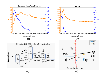
Furthermore, the simulated structure is a fully textured one, as shown in Fig. 1(a). To find the best PCE, the structure of the device is optimized by trying different values for the period and amplitude . In addition, the materials selected for our simulated structure are based on experimental results for PVK/c-Si TSCs published by Hou et al.Hou et al. (2020) in 2020. The two main absorption layers comprise PVK () and crystalline silicon (c-Si; 250 m), with (140 nm) for the antireflection film, IZO (100 nm) for the top electrode, (20 nm), (20 nm), and n-type a-Si (8 nm) for the electron transport layer (ETL), (17 nm) and p-type a-Si (6 nm) for the hole transport layer (HTL), intrinsic a-Si (13 nm) and (40 nm) for the recombination junction, and ITO (150 nm) and Ag (250 nm) for the back electrodes. Figures 2(a) and 2(b) show the refractive index and extinction coefficient of the two main absorption layers used in the RCWA simulation.
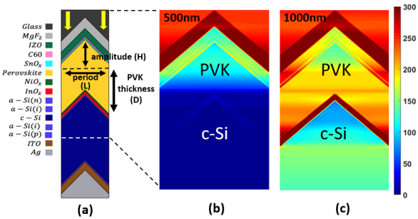
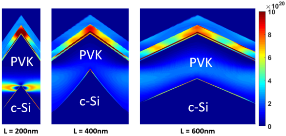
The optical field distributions in Figs. 1(b) and 1(c) reveal that short-wavelength (500 nm) light is absorbed after passing through the PVK layer and is not transmitted to the bottom cell, whereas long-wavelength (1000 nm) light passes through the PVK layer and continues to be transmitted to the silicon layer for absorption.
II.2 Simulation of electrical properties
The 2D Poisson-DD solver Huang et al. (2022); Huang, Chang, and Wu (2019); Chen and Wu (2017) is used to analyze the characteristics of PVK/Si TSCs. Having obtained the optical field distribution, the TE and TM generation rates of the electron–hole pairs in the overall device are calculated as follows:
| (5) |
| (6) |
| (7) |
where and are the generation rates determined by the electric field and magnetic field separately, is the photon frequency, is the Poynting vector, is the refractive index, is the extinction coefficient, and and are the steady-state electric field and magnetic field obtained from the RCWA solver as already mentioned.
is then passed to the 2D Poisson-DD solver to simulate the electrical characteristics of the device. The main governing equations are as follows:
| (8) |
| (9) |
| (10) |
| (11) |
where is the dielectric constant of the element at different positions, is the potential of the element, and and are the electron and hole densities, respectively. For the drift-diffusion equations, and are the electron and hole currents, respectively, and are the electron and hole mobilities, respectively, and and are the electron and hole diffusion coefficients, respectively. is the recombination rate [see (12) and (13)] determined by the Shockley–Read–Hall (SRH) nonradiative recombination and radiative recombination coefficient :
| (12) |
| (13) |
where and are the nonradiative carrier lifetimes, is the Auger coefficient, and is the intrinsic carrier concentration.
For the carrier exchange between the top and bottom cells, as shown in Fig. 2(d), a tunneling junction is designed between the PVK and c-Si absorption layers. To model the tunneling junction, the defect state-assisted tunneling recombination mechanism needs to be incorporated into the simulation to make the tunneling junction work. Hence, the tail state models at the tunneling junction are applied to study the tunneling effects. These models assume a Gaussian distribution density of defect states inside the bandgap region where carriers can hop into these defect states in the tunneling depletion region and recombine. This approach is used to simulate the carrier tunneling through the junction. The detailed model related to the tail state model we developed is in Ref. Huang et al. (2020a, b, 2023).
III Results and Discussion
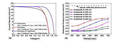
Before optimizing the texture structure of the device, we seek to calibrate our electrical results to the experimental results for the planar structure, and the characteristic parameters are compared in Table 1. As shown in Fig. 3(a), the fitting of the characteristic parameters to the experimental values is quite close. After the fitting, we realized that the value in the referenced experimental paper is quite small compared to those for other planar PVK/Si TSCs, in which can reach 1.9 V.Al-Ashouri et al. (2020) So, we improved the tunneling junction quality by increasing the defect-assisted tunneling concentration to reach higher , as shown in Fig. 3(a).
| [mA/cm2] | [V] | FF [] | PCE [] | |
|---|---|---|---|---|
| ExperimentHou et al. (2020) | 17.9 | 1.66 | 68 | 20.3 |
| Simulation | 17.9 | 1.66 | 71 | 21.3 |
| ExperimentAl-Ashouri et al. (2020) | 19.2 | 1.9 | 79 | 29.1 |
| Simulation (TJ opt.) | 17.9 | 1.91 | 75 | 25.8 |
The bandgaps of PVK and Si as the two main absorption layers are 1.68 eV and 1.12 eV, respectively, so the optimized value of V is already close to the theoretical value. To improve the PCE of the planar TSCs, must be increased. By adding a triangular texture surface, the reflected photocurrent can be reduced effectively: compared with planar structures, TSCs with texture surfaces have a reflected photocurrent that is reduced from ca. 4.5 mA/cm2 to less than 2 mA/cm2, as shown in Fig. 3(b). Also, different triangular structures reduce the photocurrent by different amounts, so the texture structure must be optimized, and before doing so, the current matching of 2T TSCs is an important issue.
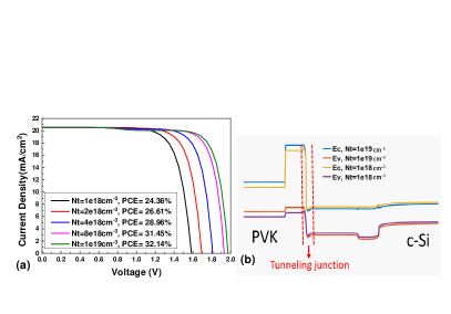
In addition to adjusting the PVK lifetime, which affects because of nonradiative recombination, another important mechanism by which 2T TSCs affect the PCE is the tunneling junction between the two cells. Improving the tunneling junction by increasing the defect-assisted tunneling concentration can improve significantly, as shown in Fig. 4(a). The period L and amplitude H used in Fig. 4 are 500nm and 400nm, repectively.
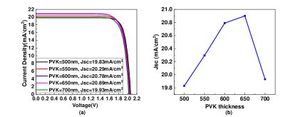
In this 2T textured PVK/c-Si TSC, the c-Si thickness is fixed at 250 m while the PVK thickness is adjusted from 500 nm to 700 nm. Figure 5(a) shows that a PVK layer that is either too thick or too thin results in a current mismatch, leading to a decrease in . It can be concluded that a PVK thickness of 650 nm is best for current matching; at this thickness, the device exhibits the highest of 20.89 mA/cm2, as shown in Fig. 5(b).
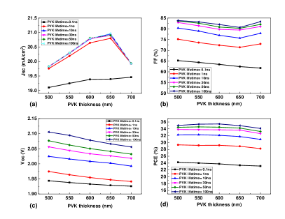
The PVK lifetime is adjusted from 0.1 ns to 100 ns in the structure with the five different values of PVK thickness mentioned above to determine whether it can improve the current mismatch caused by inappropriate PVK thickness. As shown in Fig. 6(d), except for the PVK lifetime of 0.1 ns, the longer lifetimes all exhibit a similar trend in each characteristic parameter, and the optimum PCE is achieved with a PVK thickness of 600 nm. For the 0.1-ns case, the best PCE is obtained with a PVK thickness of 500 nm, and this could be because a lifetime of 0.1 ns is too short compared to 100 ns, resulting in significant nonradiative recombination within the PVK layer, as shown in Fig. 7(a). This also results in a significant decrease in , as shown in Fig. 6(a).
| 650 | 675 | 700 | 700 | 700 | 675 | |
| 700 | 750 | 725 | 725 | 750 | 750 | |
| 750 | 800 | 775 | 675 | 625 | 700 | |
| 700 | 650 | 750 | 625 | 600 | 700 | |
| 700 | 675 | 550 | 625 | 600 | 700 |
Having discussed the importance of current matching, we now seek to optimize the triangular texture structure with different value of amplitude and period . While optimizing the texture structure, we also adjust the PVK thickness so that all structural devices are under current-matching conditions to ensure the best efficiency performance. The PVK thickness of each device under current-matching conditions is given in Table 2.
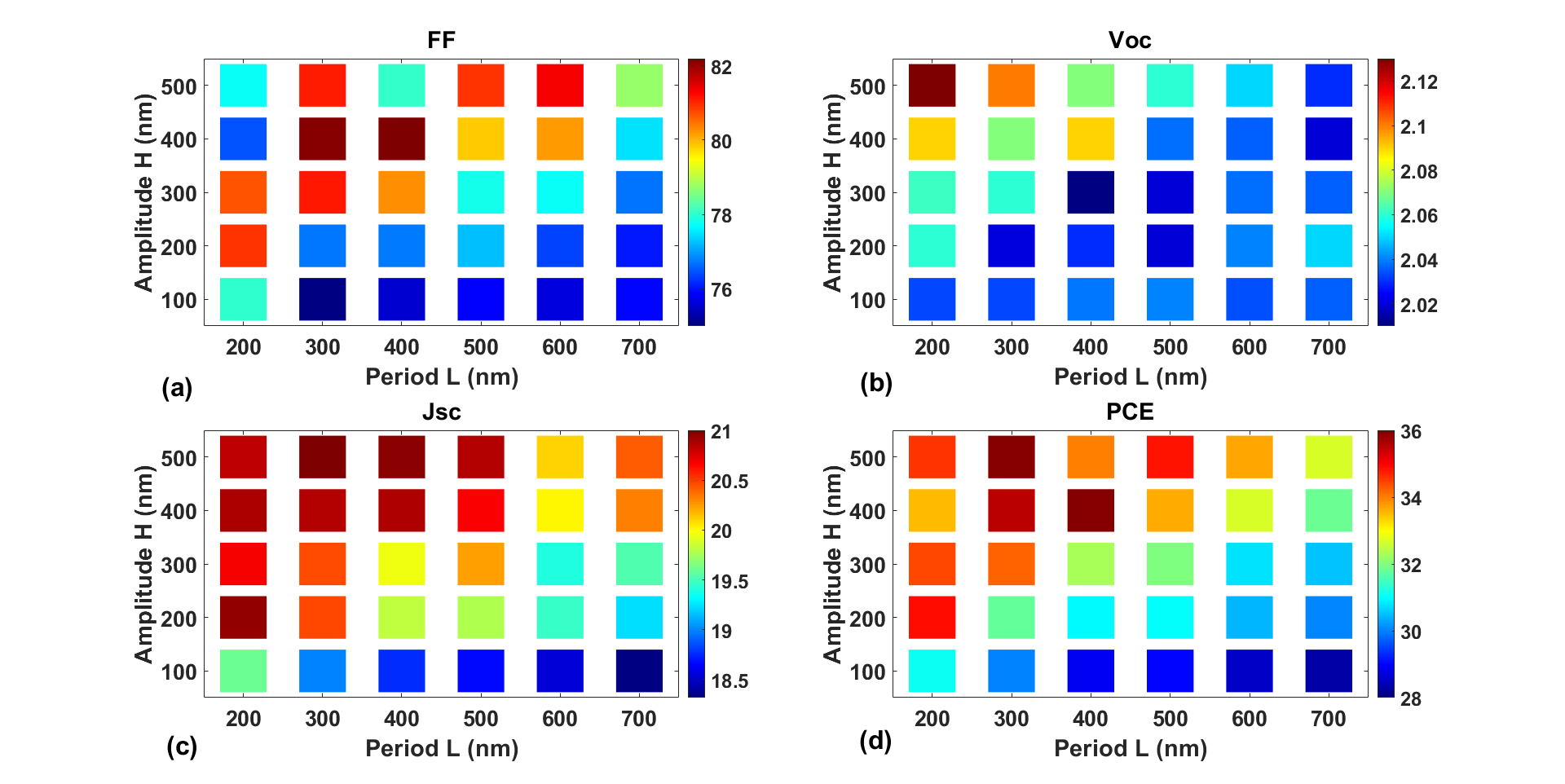
As already mentioned, when the tip angle of the triangular texture structure is smaller, there will be less reflected photocurrent, and Fig. 8(c) shows that in the electrical results also conforms to the same trend. The PCE map in Fig. 8(d) shows that the best efficiency is that of the structure with nm and nm.
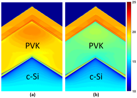
Fixing nm, we use the three structures with nm, 400 nm, and 600 nm to discuss how affects the PCE. Table 3 shows that the decrease in for the structure with nm may be due to the larger reflected photocurrent mentioned earlier. There is no significant difference in among the three structures. The main reason for the difference in PCE between the structures with nm and 400 nm is that the nonradiative recombination of the PVK absorption layer at the maximum power point voltage for nm is larger, as shown in Fig. 9, which leads to a decrease in fill factor (FF), making the overall device efficiency lower than that of the structure with nm. Also, it can be seen that in the PVK layer of the structure with nm, the overall nonradiative recombination is slightly larger than that for the structure with nm, causing the FF to decrease slightly by 2%.
| [mA/cm2] | [V] | FF [] | PCE [] | |
|---|---|---|---|---|
| nm, nm | 20.88 | 2.09 | 76 | 33.5 |
| nm, nm | 20.87 | 2.09 | 82 | 35.9 |
| nm, nm | 20.01 | 2.03 | 80 | 32.6 |
IV Conclusion
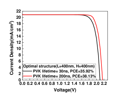
The main focus herein was exploring the optimization of the texture structure for 2T PVK/Si TSCs. From the electrical results, the optimal structure with the highest PCE of 38.13% is that with nm and nm. Furthermore, if the PVK lifetime can be increased from 30 ns to 200 ns, then can be improved from 2.09 V to 2.16 V to obtain a higher PCE of 38.13%. Therefore, achieving the anticipated efficiency levels outlined in this research depends on upcoming efforts to construct the suggested texture structure. It is essential to focus on improving the quality of PVK materials and enhancing the tunneling junction. In the future, 2T PVK/Si TSCs could reach an efficiency of ca. 38%.
V DATA AVAILABILITY
The data that support the findings of this study are available from the corresponding author upon reasonable request. The simulation tool with all functions used in this software can be download in https://yrwu-kw.ee.ntu.edu.tw for free in academic use.
Acknowledgements.
This work was supported by the National Science and Technology Council (Grant Nos. 112-2221-E-002-214-MY3 and 112-2221-E-002 -215-MY3, and 112-2923-E-002-002).References
References
- Saliba et al. (2016a) M. Saliba, T. Matsui, J.-Y. Seo, K. Domanski, J.-P. Correa-Baena, M. K. Nazeeruddin, S. M. Zakeeruddin, W. Tress, A. Abate, A. Hagfeldt, et al., “Cesium-containing triple cation perovskite solar cells: improved stability, reproducibility and high efficiency,” Energy & environmental science 9, 1989–1997 (2016a).
- Singh and Miyasaka (2018) T. Singh and T. Miyasaka, “Stabilizing the efficiency beyond 20% with a mixed cation perovskite solar cell fabricated in ambient air under controlled humidity,” Advanced Energy Materials 8, 1700677 (2018).
- Saliba et al. (2016b) M. Saliba, T. Matsui, K. Domanski, J.-Y. Seo, A. Ummadisingu, S. M. Zakeeruddin, J.-P. Correa-Baena, W. R. Tress, A. Abate, A. Hagfeldt, et al., “Incorporation of rubidium cations into perovskite solar cells improves photovoltaic performance,” Science 354, 206–209 (2016b).
- Abdi-Jalebi et al. (2018) M. Abdi-Jalebi, Z. Andaji-Garmaroudi, S. Cacovich, C. Stavrakas, B. Philippe, J. M. Richter, M. Alsari, E. P. Booker, E. M. Hutter, A. J. Pearson, et al., “Maximizing and stabilizing luminescence from halide perovskites with potassium passivation,” Nature 555, 497–501 (2018).
- Yoo et al. (2021) J. J. Yoo, G. Seo, M. R. Chua, T. G. Park, Y. Lu, F. Rotermund, Y.-K. Kim, C. S. Moon, N. J. Jeon, J.-P. Correa-Baena, et al., “Efficient perovskite solar cells via improved carrier management,” Nature 590, 587–593 (2021).
- Jiang et al. (2022) Q. Jiang, J. Tong, Y. Xian, R. A. Kerner, S. P. Dunfield, C. Xiao, R. A. Scheidt, D. Kuciauskas, X. Wang, M. P. Hautzinger, et al., “Surface reaction for efficient and stable inverted perovskite solar cells,” Nature 611, 278–283 (2022).
- Qiu et al. (2018) Z. Qiu, Z. Xu, N. Li, N. Zhou, Y. Chen, X. Wan, J. Liu, N. Li, X. Hao, P. Bi, et al., “Monolithic perovskite/si tandem solar cells exceeding 22% efficiency via optimizing top cell absorber,” Nano Energy 53, 798–807 (2018).
- Wu et al. (2017) Y. Wu, D. Yan, J. Peng, Y. Wan, S. P. Phang, H. Shen, N. Wu, C. Barugkin, X. Fu, S. Surve, et al., “Monolithic perovskite/silicon-homojunction tandem solar cell with over 22% efficiency,” Energy & Environmental Science 10, 2472–2479 (2017).
- Bush et al. (2017) K. A. Bush, A. F. Palmstrom, Z. J. Yu, M. Boccard, R. Cheacharoen, J. P. Mailoa, D. P. McMeekin, R. L. Hoye, C. D. Bailie, T. Leijtens, et al., “23.6%-efficient monolithic perovskite/silicon tandem solar cells with improved stability,” Nature Energy 2, 1–7 (2017).
- Chen et al. (2016) B. Chen, Y. Bai, Z. Yu, T. Li, X. Zheng, Q. Dong, L. Shen, M. Boccard, A. Gruverman, Z. Holman, et al., “Efficient semitransparent perovskite solar cells for 23.0%-efficiency perovskite/silicon four-terminal tandem cells,” Advanced Energy Materials 6, 1601128 (2016).
- Filipič et al. (2015) M. Filipič, P. Löper, B. Niesen, S. De Wolf, J. Krč, C. Ballif, and M. Topič, “ perovskite/silicon tandem solar cells: characterization based optical simulations,” Optics express 23, A263–A278 (2015).
- Foster and John (2016) S. Foster and S. John, “Light-trapping design for thin-film silicon-perovskite tandem solar cells,” Journal of Applied Physics 120 (2016).
- Löper et al. (2015) P. Löper, S.-J. Moon, S. M. De Nicolas, B. Niesen, M. Ledinsky, S. Nicolay, J. Bailat, J.-H. Yum, S. De Wolf, and C. Ballif, “Organic–inorganic halide perovskite/crystalline silicon four-terminal tandem solar cells,” Physical Chemistry Chemical Physics 17, 1619–1629 (2015).
- Mailoa et al. (2015) J. P. Mailoa, C. D. Bailie, E. C. Johlin, E. T. Hoke, A. J. Akey, W. H. Nguyen, M. D. McGehee, and T. Buonassisi, “A 2-terminal perovskite/silicon multijunction solar cell enabled by a silicon tunnel junction,” Applied Physics Letters 106 (2015).
- McMeekin et al. (2016) D. P. McMeekin, G. Sadoughi, W. Rehman, G. E. Eperon, M. Saliba, M. T. Hörantner, A. Haghighirad, N. Sakai, L. Korte, B. Rech, et al., “A mixed-cation lead mixed-halide perovskite absorber for tandem solar cells,” Science 351, 151–155 (2016).
- Werner et al. (2016) J. Werner, C.-H. Weng, A. Walter, L. Fesquet, J. P. Seif, S. De Wolf, B. Niesen, and C. Ballif, “Efficient monolithic perovskite/silicon tandem solar cell with cell area 1 ,” The journal of physical chemistry letters 7, 161–166 (2016).
- Aydin et al. (2023) E. Aydin, E. Ugur, B. K. Yildirim, T. G. Allen, P. Dally, A. Razzaq, F. Cao, L. Xu, B. Vishal, A. Yazmaciyan, et al., “Enhanced optoelectronic coupling for perovskite-silicon tandem solar cells,” Nature , 1–3 (2023).
- Mariotti et al. (2023) S. Mariotti, E. Köhnen, F. Scheler, K. Sveinbjörnsson, L. Zimmermann, M. Piot, F. Yang, B. Li, J. Warby, A. Musiienko, et al., “Interface engineering for high-performance, triple-halide perovskite–silicon tandem solar cells,” Science 381, 63–69 (2023).
- Chin et al. (2023) X. Y. Chin, D. Turkay, J. A. Steele, S. Tabean, S. Eswara, M. Mensi, P. Fiala, C. M. Wolff, A. Paracchino, K. Artuk, et al., “Interface passivation for 31.25%-efficient perovskite/silicon tandem solar cells,” Science 381, 59–63 (2023).
- Al-Ashouri et al. (2020) A. Al-Ashouri, E. Köhnen, B. Li, A. Magomedov, H. Hempel, P. Caprioglio, J. A. Márquez, A. B. Morales Vilches, E. Kasparavicius, J. A. Smith, et al., “Monolithic perovskite/silicon tandem solar cell with> 29% efficiency by enhanced hole extraction,” Science 370, 1300–1309 (2020).
- Leijtens et al. (2018) T. Leijtens, K. A. Bush, R. Prasanna, and M. D. McGehee, “Opportunities and challenges for tandem solar cells using metal halide perovskite semiconductors,” Nature Energy 3, 828–838 (2018).
- Kang and Park (2019) D.-H. Kang and N.-G. Park, “On the current–voltage hysteresis in perovskite solar cells: dependence on perovskite composition and methods to remove hysteresis,” Advanced Materials 31, 1805214 (2019).
- Zhao et al. (2019) Q. Zhao, A. Hazarika, X. Chen, S. P. Harvey, B. W. Larson, G. R. Teeter, J. Liu, T. Song, C. Xiao, L. Shaw, et al., “High efficiency perovskite quantum dot solar cells with charge separating heterostructure,” Nature communications 10, 2842 (2019).
- Yablonovitch and Cody (1982) E. Yablonovitch and G. D. Cody, “Intensity enhancement in textured optical sheets for solar cells,” IEEE Transactions on electron devices 29, 300–305 (1982).
- Brongersma, Cui, and Fan (2014) M. L. Brongersma, Y. Cui, and S. Fan, “Light management for photovoltaics using high-index nanostructures,” Nature materials 13, 451–460 (2014).
- Sahli et al. (2018) F. Sahli, J. Werner, B. A. Kamino, M. Bräuninger, R. Monnard, B. Paviet-Salomon, L. Barraud, L. Ding, J. J. Diaz Leon, D. Sacchetto, et al., “Fully textured monolithic perovskite/silicon tandem solar cells with 25.2% power conversion efficiency,” Nature materials 17, 820–826 (2018).
- Walker et al. (2013) A. W. Walker, O. Thériault, M. M. Wilkins, J. F. Wheeldon, and K. Hinzer, “Tunnel-junction-limited multijunction solar cell performance over concentration,” IEEE Journal of Selected Topics in Quantum Electronics 19, 1–8 (2013).
- Yamaguchi (2003) M. Yamaguchi, “Iii–v compound multi-junction solar cells: present and future,” Solar energy materials and solar cells 75, 261–269 (2003).
- Varache et al. (2015) R. Varache, C. Leendertz, M. Gueunier-Farret, J. Haschke, D. Muñoz, and L. Korte, “Investigation of selective junctions using a newly developed tunnel current model for solar cell applications,” Solar Energy Materials and Solar Cells 141, 14–23 (2015).
- Huang et al. (2022) J.-Y. Huang, Y.-W. Yang, W.-H. Hsu, E.-W. Chang, M.-H. Chen, and Y.-R. Wu, “Influences of dielectric constant and scan rate on hysteresis effect in perovskite solar cell with simulation and experimental analyses,” Scientific Reports 12, 7927 (2022).
- Chen and Wu (2017) S.-F. Chen and Y.-R. Wu, “A design of intermediate band solar cell for photon ratchet with multi-layer mos2 nanoribbons,” Applied Physics Letters 110 (2017).
- Pai and Wu (2022) H.-C. Pai and Y.-R. Wu, “Investigating the high field transport properties of Janus WSSe and MoSSe by DFT analysis and Monte Carlo simulations,” Journal of Applied Physics 131, 144303 (2022), https://pubs.aip.org/aip/jap/article-pdf/doi/10.1063/5.0088593/16456429/144303_1_online.pdf .
- Hou et al. (2020) Y. Hou, E. Aydin, M. De Bastiani, C. Xiao, F. H. Isikgor, D.-J. Xue, B. Chen, H. Chen, B. Bahrami, A. H. Chowdhury, et al., “Efficient tandem solar cells with solution-processed perovskite on textured crystalline silicon,” Science 367, 1135–1140 (2020).
- Huang, Chang, and Wu (2019) J.-Y. Huang, E.-W. Chang, and Y.-R. Wu, “Optimization of mapbi -based perovskite solar cell with textured surface,” IEEE Journal of Photovoltaics 9, 1686–1692 (2019).
- Huang et al. (2020a) J.-Y. Huang, M.-T. Wang, G.-Y. Chen, J.-Y. Li, S.-P. Chen, J.-H. Lee, T.-L. Chiu, and Y.-R. Wu, “Analysis of the triplet exciton transfer mechanism at the heterojunctions of organic light-emitting diodes,” Journal of Physics D: Applied Physics 53, 345501 (2020a).
- Huang et al. (2020b) J.-Y. Huang, J.-H. Lee, Y.-R. Wu, T.-Y. Chen, Y.-C. Chiu, J.-J. Huang, M.-k. Leung, and T.-L. Chiu, “Revealing the mechanism of carrier transport in host-guest systems of organic materials with a modified poisson and drift-diffusion solver,” Physical Review Materials 4, 125602 (2020b).
- Huang et al. (2023) J.-Y. Huang, H.-C. Hung, K.-C. Hsu, C.-H. Chen, P.-H. Lee, H.-Y. Lin, B.-Y. Lin, M.-k. Leung, T.-L. Chiu, J.-H. Lee, et al., “Numerical analysis and optimization of a hybrid layer structure for triplet–triplet fusion mechanism in organic light-emitting diodes,” Advanced Theory and Simulations 6, 2200633 (2023).