GdAlSi: An antiferromagnetic topological Weyl semimetal with non-relativistic spin splitting
Abstract
Spintronics has emerged as a viable alternative to traditional electronics based technologies in the past few decades. While on one hand, the discovery of topological phases of matter with protected spin-polarized states has opened up exciting prospects, recent revelation of intriguing non-relativistic spin splitting in collinear antiferromagnetic materials with unique symmetries facilitate a wide possibility of realizing both these features simultaneously. In this work, we report the co-existence of these two intriguing properties within a single material: GdAlSi. It crystallizes in a body-centered tetragonal structure with a non-centrosymmetric space group (). The magnetization data indicates antiferromagnetic ordering with an ordering temperature () 32 K. Ab-initio calculations reveal GdAlSi to be a collinear antiferromagnetic Weyl semimetal with an unconventional, momentum-dependent spin splitting, also referred to as altermagnet. Angle-resolved photoemission spectroscopy measurements on GdAlSi single crystals subsequently confirm the presence of Fermi arcs, a distinctive hallmark of Weyl semimetals. Electric and magnetic multipole analysis provides a deeper understanding of the symmetry-mediated, momentum-dependent spin splitting, which has strictly non-relativistic origin. To the best of our knowledge, such co-existence of unconventional antiferromagnetic order and non-trivial topology is unprecedented and has never been observed before in a single material, rendering GdAlSi a special and promising candidate material. We propose a device harnessing these features, poised to enable practical and efficient topotronic applications.
I Introduction
A large number of today’s technological advancements are based on extensive research in condensed matter and material physics, which bring about innovations in the field of electronics. The control and manipulation of electronic charge using different devices dominates the functioning of our day-to-day lives and hence it requires a constant push towards the hunt for more power-efficient devices with scalable architecture and simple configurations. Spintronics brings a key player along these lines, dictated by the intrinsic spin of electrons. The control and manipulation of this extra degree of freedom along with the charge of electrons has proved to be promising with several proof-of-concept devices, taking us a few steps closer to surpassing semiconductor junctions in mainstream technological applications.
Conventionally, materials with ferromagnetic (FM) order have been the primary choice for spintronic based devices due to their inherent spin polarization [inomata2008highly, hirohata2014future], a consequence of exchange splitting. But these materials are sensitive to external stray fields when used in devices. Materials with antiferromagnetic (AFM) order can overcome such shortcomings [jungwirth2016antiferromagnetic, baltz2018antiferromagnetic], but for collinear ordering, there is a distinct absence of any spin polarization due to the mirror symmetric density of states arising out of combined inversion () and time-reversal () symmetries. This can be resolved via specific materials hosting non-collinear AFM order which lifts the spin degeneracy along with a fully compensated magnetic moment [jungwirth2016antiferromagnetic]. Interestingly, recent years have witnessed yet another class of materials which acquire certain symmetries in the crystal and magnetic structures that can lead to spin splitting in the momentum space of a collinear AFM system [Libor2020, Naka2019, Kyo-Hoon2019, Hayami2019, Yuan2020, Yuan2021, Smejkal2022, Yuan, yuan2023uncovering]. Among these, RuO2 being a classic example [Libor2020, Shao2021, Smejkal2022, PhysRevX.12.040501]. Such momentum dependent spin splitting with intimate connection to crystal symmetries can be used as efficient spin splitters leading to better spintronic applications [Hayami2019, Gonzalez2021, Bai2022, Hayami2022, Karube2022, Bose2022].
In the past few decades, the discovery of topological materials with ideally dissipationless, symmetry-protected, and robust spin-polarized surface states (SS) have generated immense interest due to their potential spintronic applications, leading to the broader topic of topotronics. These topological materials are categorized into different classes based on their topological invariants. Weyl semimetals are one such class with either broken or symmetry, that hosts Weyl Fermions as low-energy quasi-particle excitations. In WSMs, the bulk valence and conduction bands cross each other at discrete points (always occur in pairs) of definite chirality (handedness), known as Weyl nodes, while having linear dispersion around the node along all three momentum directions. Though separated in the bulk, these pairs of Weyl nodes give rise to spin-polarized Fermi arcs on the surface of a WSM which originate and terminate at surface of one such pair of Weyl nodes of opposite chirality. These characteristic features lead to the observation of exotic phenomena such as the chiral anomaly, unconventional anomalous Hall effect, and unusual magnetoresistance. Discovery of Weyl Fermions have been reported first in non-magnetic system such as TaAs [lv2015observation, PhysRevX.5.011029, xu2015discovery] and transition-metal binary/ternary chalcogenides with tilted (type-II) Weyl cones [soluyanov2015type, deng2016experimental, wu2016observation, PhysRevB.93.201101, PhysRevB.95.241108] followed by magnetic systems such as Mn3Sn [kuroda2017evidence], Co3Sn2S2 [wang2018large], and Co2MnGa [belopolski2019discovery]. Recently, unconventional WSMs have been reported in few non-centrosymmetric magnetic RAlSi/Ge (R: rare earth) [xu2017discovery, PhysRevLett.124.017202, gaudet2021weyl, li2023, sanchez2020observation]. These systems exhibit diverse electronic properties, including non-trivial topology and strong correlations [xu2017discovery, sanchez2020observation]. As such, they provide a great platform to investigate the interplay between Weyl fermions and exotic magnetic order, as both the broken and symmetries play a role in mediating Weyl fermionic states. In contrast to previous reports on RAlSi/Ge where the light rare earth elements have smaller magnetic moments (), GdAlSi with the largest moment () is an ideal candidate to study such an interplay.
In this article, we present a combined first-principle calculation, angle-resolved photoemission spectroscopy (ARPES) and magneto-transport studies of the emergent topological phases in non-centrosymmetric unconventional antiferromagnetic WSM GdAlSi. The purpose of this study is two-fold. Firstly, we predict the presence of an unconventional WSM phase in GdAlSi using ab-initio calculations and verified the same using the ARPES measurements. Secondly we propose the presence of momentum dependent spin splitting with a strong non-relativistic origin in a non-centrosymmetric collinear AFM as confirmed from electric and magnetic multipole studies.[Naka2019, Hayami2019] This effect is sometimes nomenclatured as ‘altermagnetism’ [Libor2020, Naka2019, Kyo-Hoon2019, Hayami2019, Yuan2020, Yuan2021, Smejkal2022, Yuan, yuan2023uncovering] which has never been observed in a non-centrosymmetric system. We also analysed the effects of such splitting on non-trivial band topology. Overall, GdAlSi is the first exclusive candidate material which co-host both altermagnetism and topological non-trivial features arising out of a unique interplay between magnetic order, topology and electronic correlations. Finally, we propose a device architecture which can leverage such unique interplay for practical spintronic/topotronic applications. Our systematic study not only contributes to a better understanding of non-trivial topology of GdAlSi but also sheds new light on the intimate relation between magnetic order and topology.
II Experimental and theoretical details
II.1 Single crystal growth
High-quality single crystals of GdAlSi were grown using the self-flux method in regular alumina crucibles with stoichiometric mixtures of Gd:Al:Si=1:15:1 of constituent elements having a purity of 99.99. The alumina crucibles were sealed in quartz ampules and heated up to 1000∘ C for 36 hours at a rate of 3∘C/hour and were slowly cooled down to 700 ∘C at a rate of 0.05∘ C/min for the centrifuge to remove the residual Al flux.
II.2 Angle-resolved photoemission spectroscopy (ARPES)
ARPES measurements were conducted at the BL-1 beamline in the Hiroshima Synchrotron Radiation Center (HiSOR), utilizing a hemispherical electron analyzer (VG-SCIENTA, R4000), in the vacuum ultraviolet (VUV) range of 40-65 eV. The base pressure of the ARPES chamber was maintained at 4 10-9 Pa. Energy and angular resolutions for ARPES were set at 40 meV and 0.1∘, respectively. The beam spot size was 1030 m. The temperature during measurements was kept below 30 K.
II.3 Computational details
To investigate the electronic structure of GdAlSi in different magnetic configurations, ab-initio calculations were performed within the density functional theory (DFT) framework [hohenberg_kohn1964, kohn_sham1965] using the Vienna Ab-initio Simulation Package (VASP) [kresse1996efficient, kresse1996efficiency, kresse1993ab], based on the projector-augmented wave (PAW) [blochl1994, kresse1999ultrasoft] method.
The Perdew, Burke, and Ernzerhof (PBE) [perdew1996generalized] exchange-correlation potential within the generalized gradient approximation (GGA) was employed. Calculations are performed both with and without spin-orbit coupling (SOC). A Hubbard U of 7.0 eV was applied on the Gd site using Dudarev’s method [dudarev1998] to capture the correlation effects. Brillouin zone (BZ) integration was performed on a 121212 -centered -mesh using the tetrahedron method with the total energy convergence criteria set to eV. A plane wave energy cutoff of 380 eV was used for all the calculations. The experimental crystal structure was fully optimized until the total forces on individual atoms were less than 0.001 eV/Å. A tight-binding Hamiltonian was constructed from pre-converged DFT results using the Wannier90 [PhysRevB.56.12847, PhysRevB.65.035109, RevModPhys.84.1419, wannier90, wannier90_new] package. A total of 120 bands were wannierized to calculate the (001)-surface state, with projections on atomic sites including Gd (), Al (), and Si () orbitals. The iterative Green’s function approach [lee1981_1, lee1981_2, sancho1984, sancho1985] was used to calculate the surface dispersion and Fermi surface (FS) using a semi-infinite slab as implemented in the WannierTools [wu2018wanniertools] package.
To compute the atomic-site charge ( even) and magnetic ( odd) multipoles, we decompose the calculated density matrix [Cricchio2009, Spaldin2013] into tensor moments. The symmetric (even parity) multipoles have contributions from even terms, while the broken symmetric (odd parity) multipoles have only contributions from odd terms. For the even and odd parity multipoles at the Gd atoms, we, therefore, evaluate and matrix element contributions.
III Results and discussion
III.1 Crystal structure
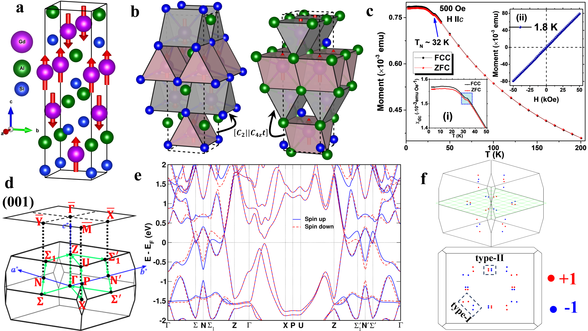
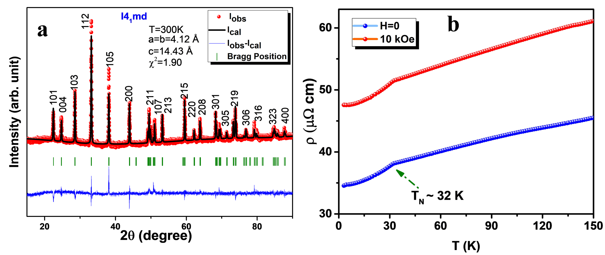
The ternary compound GdAlSi crystallizes in a body-centered tetragonal (BCT) structure (space group (), point group ) with lattice parameters Å and Å, as determined from powder XRD data (see a more detailed crystal structure analysis using Rietveld refinement along with Laue pattern and elemental analysis in Figs. S1, S2(a) and Table S1 of SM [supplement]). The structure consists of two Gd, two Al, and two Si atoms in the primitive BCT cell. Figure 1(a) displays the tetragonal conventional unit cell. An important feature of the crystal structure is the in-equivalent environments of Al and Si ions around the Gd sublattices forming a prism-like network. In particular, both GdAl6 and GdSi6 units around the two Gd sublattices are related to each other by a rotational symmetry (axis of rotation coinciding with the -axis of the tetragonal cell). More interestingly, the GdAl6 and GdSi6 units around the same Gd sublattice are also rotated with respect to each other, as depicted by pink and grey prism-like polyhedra in Fig. 1(b). These in-equivalent environments play a crucial role in driving the non-relativistic spin splitting (NRSS) as well as its manipulation in GdAlSi.
III.2 Magnetization
Figure 1(c) shows M(T) and M(H) data along with the dc magnetic susceptibility for GdAlSi. It shows a noticeable deviation at 32 K, indicated by a kink that corresponds to the onset of antiferromagnetic ordering (see the highlighted blue dashed square of inset (i)). The sharpness of the transition may indicate the collinear structure. This observation is further supported by the analysis of the resistivity data, as shown in Fig. S2 (b) of SM [supplement]. Above the Néel temperature (TN = 32 K), the resistivity and susceptibility exhibit consistent behavior [bobev2005ternary]. The Curie-Weiss law yields an effective moment of 7.95 , as expected for Gd3+, along with a Weiss constant of -103 K. Non-saturating behavior (even up to 50 kOe field) of low temperature M vs. H curve (see inset of Fig. 1(c)) indicates the presence of AFM interactions in the system.
III.3 Ab-initio results
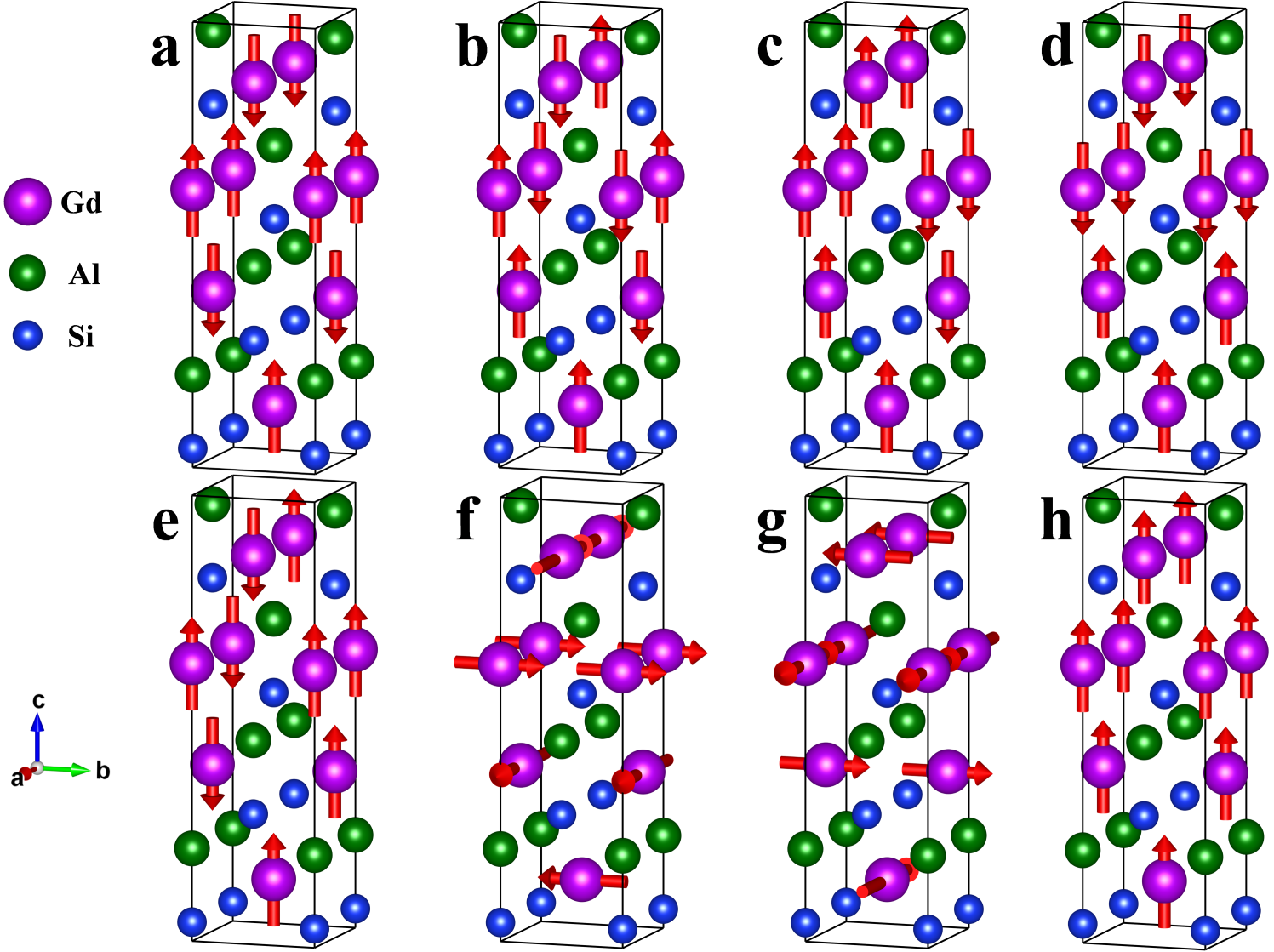
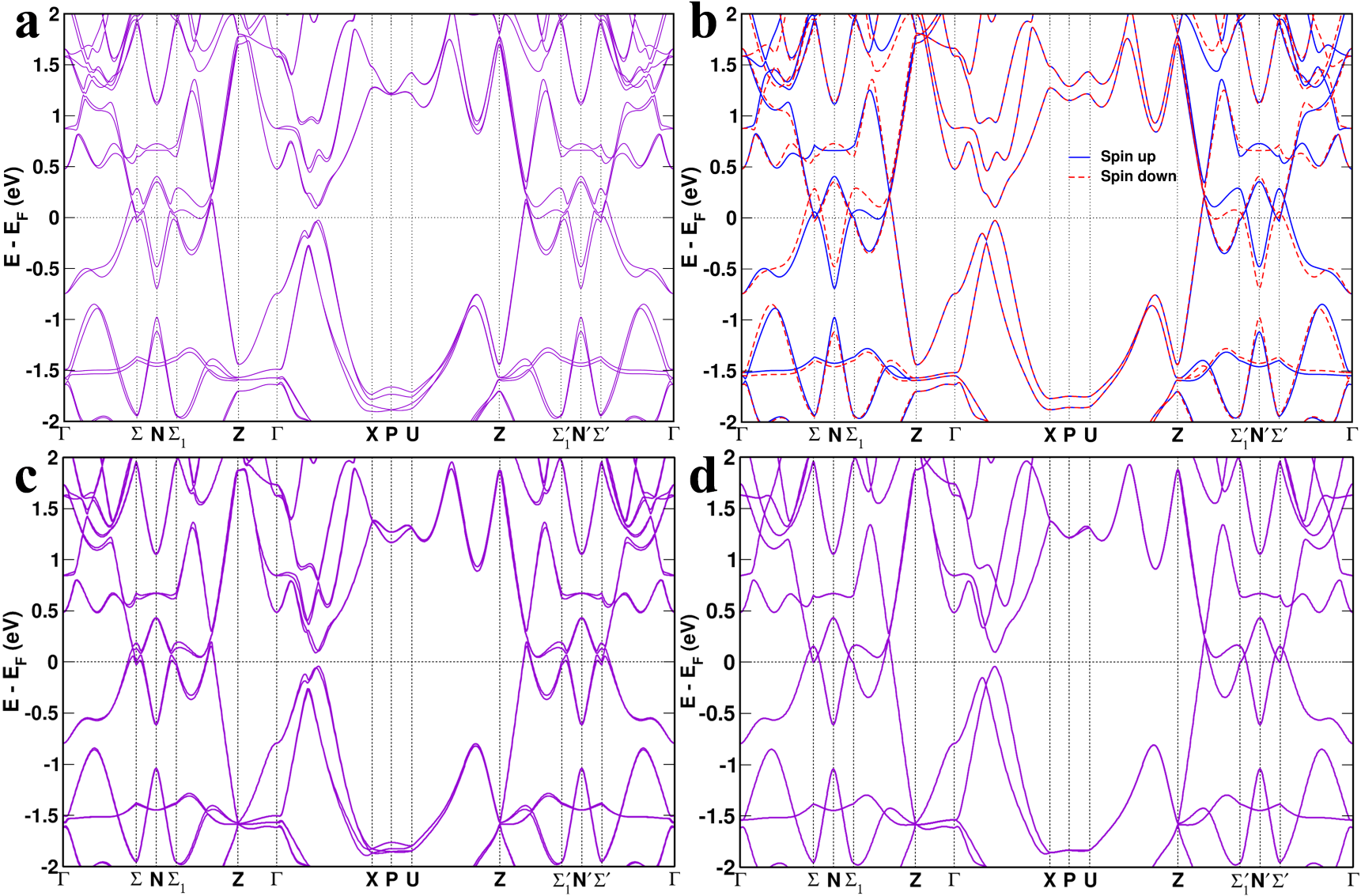
In order to investigate the electronic structure of GdAlSi, paramagnetic and various magnetic states including ferromagnetic, ferrimagnetic, antiferromagnetic, and non-collinear helical configurations (see Fig. S3 of SM [supplement]) were simulated to determine the magnetic ground state. Among these, the AFM type-I configuration (interlayer AFM ordering among Gd atoms with moments oriented along the -axis as shown in Fig. 1(a)) is found to be the energetically most favorable configuration (also see Table S2 of SM [supplement]). This corresponds to the magnetic space group . The AFM ground state arises from the alignment and coupling of localized -electrons of Gd along the -axis, leading to spin-polarization of the conduction electrons.
Figure 1(e) depicts the spin polarized electronic bulk band structure of GdAlSi without spin-orbit coupling (SOC) using theoretically optimized lattice parameters ( Å and Å). The emergence of hole pockets along and path indicates a semi-metallic nature along with a large spin splitting (230 meV at certain momenta) which is of particular interest. Interestingly this splitting is highly path-dependent (the bands along are completely degenerate) and the spin splitting flips when going from direction to direction in the BZ. These two directions are at 90∘ to each other as evident from Fig. 1(d). Presence of such alternating spin-polarization in a collinear AFM system, while absence of the same along a specific path in the BZ gives us the first hint towards a possibility of the so-called altermagnetism [Smejkal2022, PhysRevX.12.040501] in GdAlSi. Interestingly, even in the absence of Hubbard U, GdAlSi retains the AFM type-I configuration and altermagnetic band structure. This implies a spin split bulk Fermi surface with the spin-up and the spin-down being rotated by 90∘ with respect to each other (see Fig. S4 of SM [supplement]). We discuss the multipolar origin of the spin splitting and its possible manipulation later in section III.4. A projection of the bulk FS on the plane is provided in Fig. S4 of the SM [supplement] which clearly shows this. The opposite spin sublattice transformation is given by . Following the nomenclature of mejkal et al [Smejkal2022, PhysRevX.12.040501], acts on the spin-space (equivalent to leading to spin inversion) and acts on the real-space followed by a translation t. This real space transformation also acts on the reciprocal (momentum) space and leaves the momenta residing on the diagonal planes in the bulk BZ invariant leading to spin degeneracy along direction.
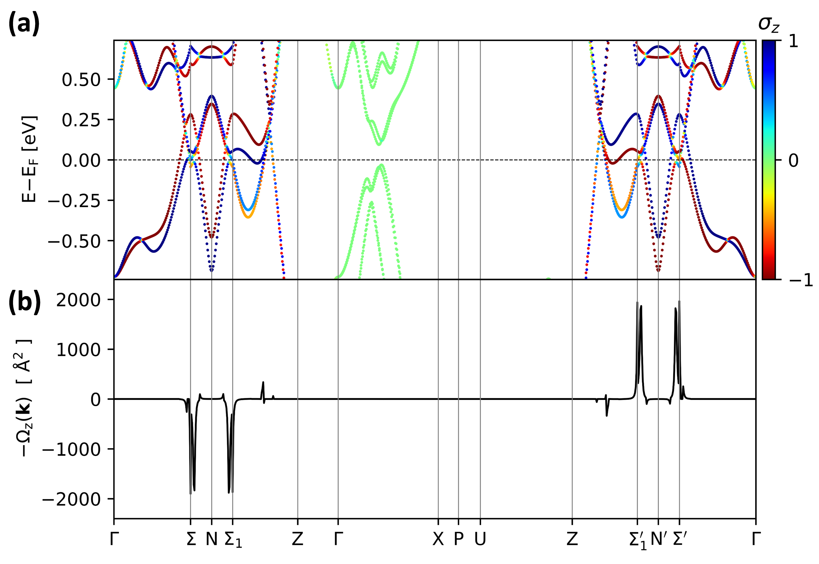
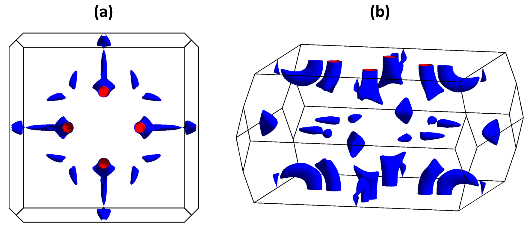
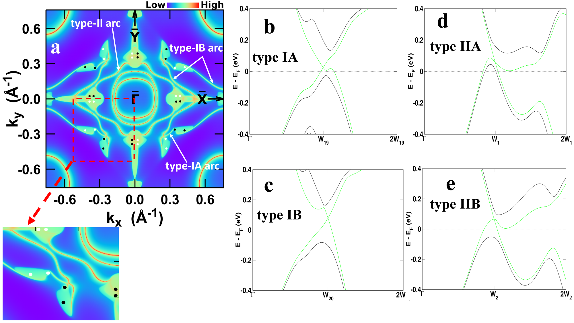
With the incorporation of SOC, although the electronic bands are slightly perturbed, the overall feature of the bands remain similar with only minor splittings (see Fig. S5 and associated discussions in section S2 of SM [supplement]) of about 70 meV at certain momenta which is relatively smaller than the non-relativistic spin splitting. The -component of spin also shows the same alternating feature seen in non-relativistic bands (see Fig. S6(a) of SM [supplement]). This can be attributed to Gd3+ being an effective -state ion (Gd, ) which implies a dominance of non-relativistic effects on the electronic properties of GdAlSi in spite of Gd3+ being a heavy ion. This also implicates the -component of spin to be a conserved quantity ( is a good quantum number) and it is further protected by symmetry of the spin-only groups [Smejkal2022, PhysRevX.12.040501] due to the collinear magnetic arrangement. Band-splitting at various crystal momenta can thus be attributed to the lack of both and symmetries along those directions in the bulk BZ. Due to SOC, avoided crossings appear near the Fermi level () along the and path leading to high intrinsic total Berry curvature. For more details, see Fig. S6(b) and associated discussions in section S2 of SM [supplement]. Further, a search of topological nodal points in the bulk BZ reveals a total of 16 pairs of Weyl points (WPs) with opposite chirality, as shown in Fig. 1(f) (top-bottom). Out of these 16 pairs, 8 pairs are of type-I while the other 8 pairs are of type-II WPs. More details of the bulk WPs can be found in Table S3 of SM [supplement]. The 3D bulk Fermi surface is shown in Fig. S7 of SM [supplement]. The type-I WPs can further be divided into 4 pairs lying at an energy meV above (referred to as type-IA) and the other 4 pairs lying at an energy meV above (referred to as type-IB). Similarly, the type-II WPs can further be divided into 4 pairs lying at an energy meV above (referred to as type-IIA) and the other 4 pairs lying at an energy meV above (referred to as type-IIB) (shown in Fig. S8 of the SM [supplement]). All the type-I WPs lie on the plane while 4 pairs of type-II WPs are distributed symmetrically above and below. Type-I WPs of the same chirality are related by inversion unlike type-II WPs. The division of the type-I and type-II WPs into sub-types is important to differentiate the nature of Fermi arcs on (001) surface. This is discussed in more details in Sec. III.5.
III.4 NRSS and the role of magnetic octupoles
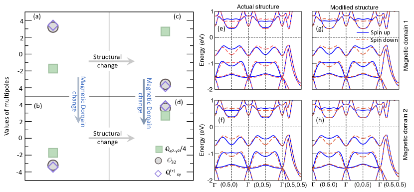
For a deeper understanding of the origin of the NRSS in GdAlSi, and to reveal its characteristics and possible manipulation, we explicitly carry out the multipole analysis. In the absence of any net magnetic dipole moment, the spin splitting has been proposed to mainly arise from higher-order magnetic multipoles [Hayami2019, HayamiPRB2020, HayamiPRB2021, Bhowal2022, Hayami2022], among which third-rank magnetic octupole, describing the anisotropy in the magnetization density, is a notable candidate. Unlike the centrosymmetric altermagnets [Smejkal2022, PhysRevX.12.040501, Mazin2022], however, GdAlSi breaks symmetry, which, in turn, also allows for ferrotype ordering of odd-parity, second-rank magnetoelectric (ME) multipole component . This leaves the origin of the NRSS in GdAlSi an open question, which we investigated here for the first time. In fact, the NRSS feature in RAlSi family, as a whole, has never been looked upon and hence might require a revisit for all those systems which are reported in the literature so far.
The computed multipoles in GdAlSi confirm the presence of a ferrotype odd-parity ME multipole component as well as ferrotype even-parity magnetic octupole components [note1] and (the latter also known as toroidal quadrupole moment), consistent with the magnetic symmetry. Interestingly, however, we find that the ferrotype has a non-zero value only in the presence of SOC, while the even-parity magnetic octupoles and exist even in the absence of SOC (see Fig. 2a). This excludes the former from being the origin of the NRSS, hinting magnetic octupoles to be the lowest-order ferroic magnetic multipole in GdAlSi in the absence of SOC.
To verify if the magnetic octupoles can describe the NRSS in GdAlSi, we analyze the corresponding reciprocal space representation. The -space representation [Watanabe2018, BhowalSpaldin2021, BhowalPRL2022] of the existing magnetic octupole components viz., with being the collinear magnetic moment along , provides the following insight into the NRSS. First of all, the representation indicates the occurrence of the spin splitting in the momentum space with non-zero and (see Fig. 2(e)), provided (see the absence of NRSS along in Fig. 2(e)). Secondly, the spin splitting is symmetric in (see the band dispersion along in Fig. 2e) as the representation is even in . We note that this is in contrast to the spin-orbit coupling driven Rashba-like spin splitting which is antisymmetric with respect to . Finally, under the rotation of the momentum direction from to , the spin splitting reverses (band dispersion along vs. in Fig. 2(e)). Thus, our computed band structure confirms all the characteristics mentioned above, predicted from the -space representation of the existing magnetic octupole moments, further supporting the magnetic octupoles to be the origin of the NRSS.
To control the NRSS, we further manipulate the magnetic octupoles. For this, we first consider the opposite magnetic domain by flipping the direction of the spins without altering the magnetic symmetry. This results in a sign-switching of the magnetic octupole as depicted in Fig. 2(b). Consequently, the spin splitting also reverses (see Fig. 2(f)). Since the inequivalent Gd ( Si, Al) environment is responsible for broken symmetry, we further artificially modify the crystal structure by interchanging the atomic positions of Al and Si to see the impact of the surrounding non-magnetic ions on the magnetic octupoles and hence the NRSS. This interchanges the inequivalent GdSi6 and GdAl6 networks, which, in turn, results in a sign change of the charge quadrupole moment (see Fig. 2(c)) with AFM ordering at the Gd ions. Interestingly, in this case, even without any change in the magnetic arrangement, we find that the magnetic octupoles change sign (see Fig. 2(c)) and, accordingly, the NRSS also reverses (see Fig. 2(g)), emphasizing the role of the surrounding non-magnetic environment on the NRSS. For this hypothetical modified structure, a change in the magnetic domain further switches the sign of the magnetic octupoles without affecting the charge quadrupole (see Fig. 2(d)). As a result, the spin splitting reverses again (see Fig. 2(h)), and we get a similar band structure as in Fig. 2(e).
III.5 Surface dispersion and Fermi surface
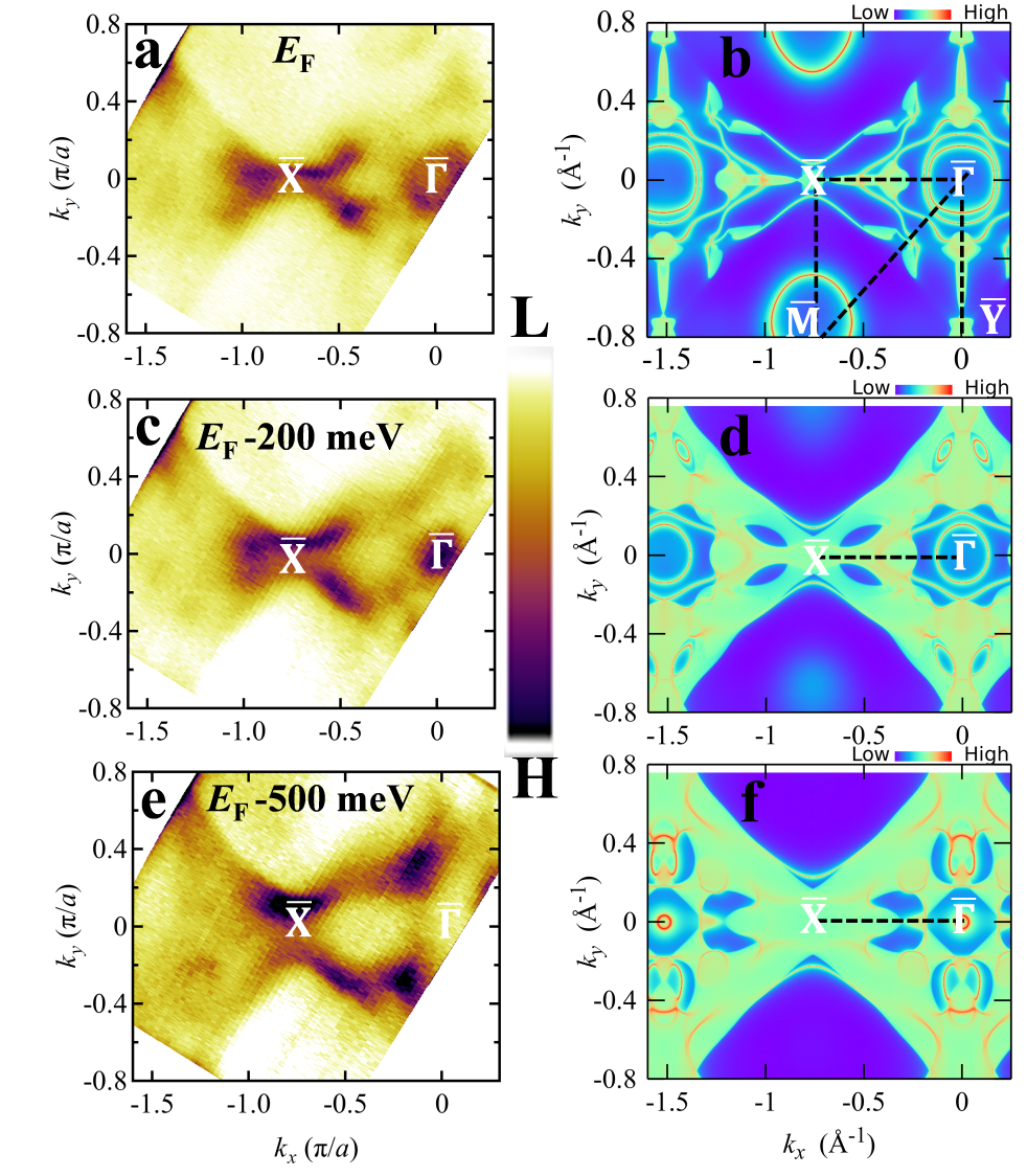
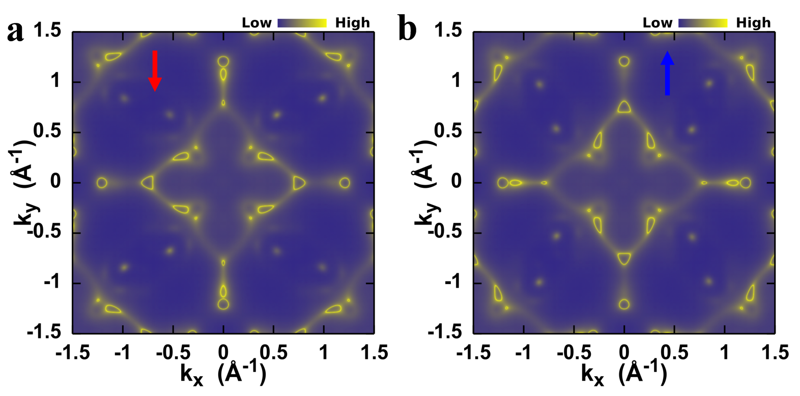
Figures 3(b) and 4(c) show the calculated Fermi surface, and band dispersion along surface high symmetry line respectively for Al-terminated (001) surface of GdAlSi. The FS is diamond-shaped with four-fold symmetry and shows several prominent features. A concentric closed contour can be seen surrounding the -point forming an electron pocket originating exclusively from the surface. Four butterfly-like surface states each containing two pairs of type-I (A,B) WPs are located along the direction. Short Fermi arcs joining the type-IA WPs and extended Fermi arcs joining the type-IB WPs can be prominently seen on the FS (shown in Fig. S8(a) of the SM [supplement]). The extended Fermi arcs also form a fish-tail like feature along the direction. There are also extended Fermi arcs joining the type-II WPs around the central pocket (shown in Fig. S8(a) of the SM [supplement]). The fish-tail like arcs along the direction persists even at deeper energies while the central pocket slowly diminishes as shown in Fig. 3 (d,f). Other surface features are masked due to emergence of bulk pockets at deeper energies. The computed FS indicates the existence of topological Fermi arcs in all four quadrants, displaying an asymmetry along the high-symmetry lines and on the surface. This asymmetry can be attributed to non-trivial band topology in GdAlSi as observed in other RAlSi/Ge compounds [sanchez2020observation, PhysRevMaterials.7.L051202]. To the best of our knowledge, AFM phase of any RAlX (X=Si,Ge) family has never been simulated in the existing literature, though few of them are experimentally confirmed to show the same. This is the first study to simulate the bulk as well as surface properties in the collinear AFM phase (magnetic ground state of GdAlSi).
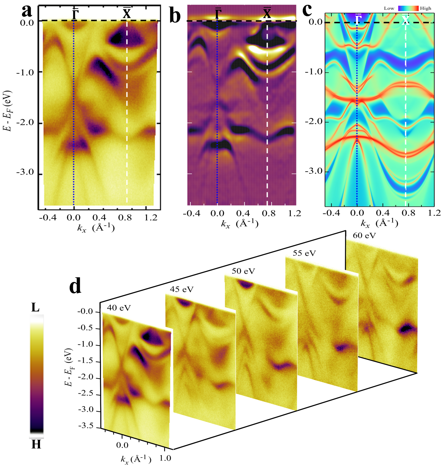
The calculated surface dispersion along path (see Fig. 4c) also shows interesting features. An electron pocket is clearly visible at -point near originating exclusively from the surface. There is a pronounced crossing at/around -1.5 eV at the edge of the bulk-energy gap and two downward parabolic band dispersion at deeper energy ( -2.0 eV, and -2.5 eV respectively) can be seen at . An upward parabolic-like band dispersion originating from the surface states at/around -1 eV and a strong surface state at/around -2.5 eV at is also visible.
III.6 VUV ARPES
Figure 3(a) displays the unsymmetrized Fermi surface derived from low-energy (VUV) ARPES measurements at 24 K, employing a photon energy of = 50 eV. Figures 3(c) and 3(e) depict the constant binding energy contours obtained at meV and meV respectively for the unsymmetrized case. Remarkably, the observed features in the FS, such as the presence of an electron pocket at , the existence of Fermi arc-like features along the - direction (diagonal) which become more pronounced at deeper energies (Fig. 3(c,e)), and a fish tail-like pattern at and a similar state at , closely resemble the features observed in the calculated Fermi surface (see Fig. 3(b)). To better understand these features, energy-momentum cuts are taken along the - direction (refer to Fig. S9 and S10 of the SM [supplement]). Further elaboration of this study can be found in the SM [supplement].
Figure 4(a) displays the intricate features observed in the band dispersion at a photon energy of 40 eV. To make the features sharper and more prominent, a second derivative image analysis was performed on Fig. 4(a), the result of which is shown in Fig. 4(b). The energy and momentum scale in the ARPES results (Fig. 4(a,b)) and the calculated results (Fig. 4(c)) are kept the same enabling a direct comparison between the measured and the simulated dispersions. To distinguish between the contributions of surface and bulk bands, photon energy dependent ARPES measurements are carried out over the photon energy range 40 to 60 eV at a temperature of 24 K, as depicted in Fig. 4(d). Notably, the ARPES measurements reveal the presence of various features, such as (i) an electron pocket-like state at (ii) a crossing-like band feature at -1.4 eV near the edge of the bulk-energy gap at (iii) two downward parabolic band dispersions at deeper energies ( -2.0 eV and -2.5 eV, respectively) at (iv) an upward parabolic-like band dispersion around -0.9 eV at , and (v) a pronounced band dispersion around -2.4 eV at . These features remain largely unchanged in terms of energy and position with respect to photon energy (see Fig. 4), confirming their origin as dominant surface states. However, some other dispersion features in close proximity to the around the point turn out to be sensitive to the photon energy, indicating their bulk nature. These observed features manifest as a continuum, providing further evidence of bulk states, which is also supported by our calculations.
III.7 Device models
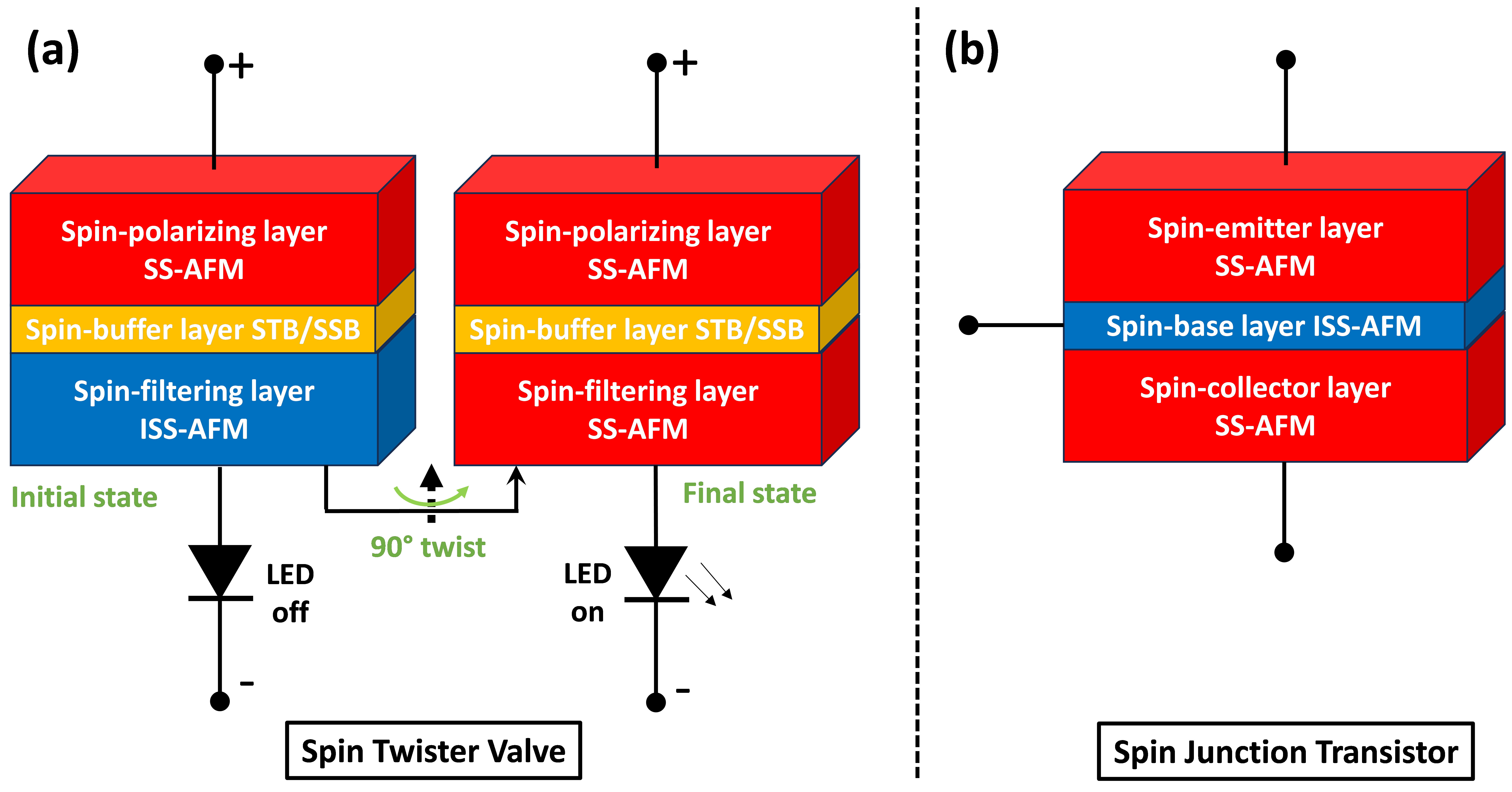
It is clearly evident that the spin polarization in GdAlSi is highly path-dependent and can be flipped by swapping the Al and Si environments around the inequivalent Gd atoms (see Sec. III.3 and III.4). This unusual feature can have interesting consequences useful for practical devices.
In case of RuO2 (another candidate for altermagnetism but centrosymmetric), it is shown that application of electric field along specific crystal directions can result in generation of highly spin polarized current [Gonzalez2021, Bai2022]. A similar response is expected in GdAlSi due to the spin anisotropy in the bulk BZ. Let us consider the Al and Si environments around the Gd atoms to have been swapped as illustrated in section III.4 such that GdAlSi now becomes the hypothetical GdSiAl. Since swapping the non-magnetic environment results in flipping of spin polarized bands (see Fig. 2(a),(c),(e),(g)), it is expected that the spin polarization in GdAlSi and GdSiAl will be opposite for a given electric field applied along a certain crystal direction.
Another interesting feature of GdAlSi and GdSiAl structures is their connection via simple crystal transformations. If one inverts the GdSiAl structure along the axis (i.e., ) and gives a transformation (rotation by 90∘ about the inverted axis) to it, one gets back the original GdAlSi structure. Our ab initio calculations show that the relative energy difference between GdAlSi and GdSiAl structures is 1 meV/atom. This implies that growing the hypothetical GdSiAl is practically feasible. Earlier studies on other RAlX family of compounds have shown a possibility of disorder among the Al and X = Si,Ge sites [bobev2005ternary, Dhar1996, Flandorfer1998, Sharma2007, Yang2020, Lyu2020].
Now if a GdAlSi layer and an inverted GdSiAl layer are sandwiched together with a spin current sensitive layer in between, one obtains what we call a spin twister valve (STV). A device architecture for the same is shown in Fig. 5(a). Here, inverted refers to inverted growth of GdSiAl layer which we believe can be achieved with current state-of-art crystal/film growth techniques. The top layer would act as a spin polarizing layer and the bottom layer as a spin filtering layer. The middle layer acts as a spin buffer layer which transfers the spin polarized current from the top to the bottom layer. This may be done in two ways. One is via a non-magnetic dielectric layer acting as a switching tunnel barrier (STB) similar to those found in magnetic tunnel junctions (MTJ). The other is via a topological insulator layer with spin polarized surface states acting as a spin-sensitive barrier (SSB). Since GdAlSi is itself a topological WSM with spin polarized Fermi arcs, this would enable surface coupling of these spin polarized states leading to ballistic spin channels and ultra-high mobility. The functioning of the device relies on the opposite spin polarizations of the top GdAlSi and the bottom inverted GdSiAl layer. When an electric field is applied across the device, initially if the top layer generates a spin-up current, then the bottom layer completely blocks it (LED off state as shown in left circuit of Fig. 5(a)). Now if the bottom layer is mechanically twisted by 90∘, it is transformed into the top layer and the spin-up current can pass through the device (LED on state as shown in right of Fig. 5(a)).
Another device architecture is possible by removing the middle layer in the proposed STV and adding another GdAlSi layer at the bottom. This would form what we call a spin junction transistor (SJT) as shown in Fig. 5(b). This would be a three-terminal device and function analogous to the semiconductor-based bipolar junction transistors (BJT) but with spin currents. The top and the bottom GdAlSi layers would behave as the spin emitter layer and the spin collector layer respectively. The sandwiched inverted GdSiAl layer would behave as the spin base layer. In a SJT, the majority and minority carriers would be spin-up and spin-down electrons (or vice-versa) respectively unlike in BJTs where the majority and minority carriers are electrons and holes (or vice-versa) respectively. The junction between the layers would act as spin depletion layers akin to depletion layers in semiconductor junctions due to the possibility of spin diffusion among the layers. When appropriately biased, one would expect SJTs to behave similar to BJTs but strictly with spin-polarized currents. The operation of such SJTs could have greater efficiency due to the presence of topological spin polarized Fermi arcs of WSMs providing spin ballistic channels. Similar to transistors which are well-known to bring technological revolution since their invention, SJTs could provide the much-awaited breakthroughs in Spintronics.
We would like to emphasize that these device architectures are entirely generic and can be extended to any spin-split antiferromagnets (SS-AFM), which in the present case is GdAlSi.
IV Conclusions
In summary, we present a comprehensive study of the electronic, magnetic and topological properties of GdAlSi employing a combined ab-initio calculations, magneto-transport and VUV ARPES measurements. This is the first system which shows the coexistence of wondrous altermagnetism feature and antiferromagnetic Weyl semimetal behavior, as confirmed by our electric/magnetic multipole analysis and ARPES measurements. Magnetic and transport measurements suggest GdAlSi to exhibit an AFM behavior below 32 K. First-principles calculations and VUV ARPES measurements confirm the presence of Fermi arc-like features, providing strong evidence of the Weyl semimetallic state. The theoretical predictions are in fair agreement with the experimental findings, further supporting the existence of Weyl points and Fermi arc-like features.
Our theoretical multipole analysis suggest the presence of altermagnetism, as indicated by significant band splitting along a specific path in the Brillouin zone. Altermagnetism has never been predicted before in rare earth materials, especially in the RAlSi family and we believe this to be the first study facilitating the same. GdAlSi has the potential to be the next promising topological/spintronic material as it offers a remarkable platform to investigate the Weyl Physics in the presence of altermagnetism and non-trivial band topology. The presence of magnetic octupoles in GdAlSi also allows for interesting physical effects such as piezomagnetism which requires future investigations. Further, we propose device models to effectively utilize this unique coexistence which can provide a new route to practical topotronic devices. Consequently, our study opens up new avenues for exploring the non-trivial band topology combined with altermagnetism with unique practical applications.
Acknowledgements.
JN acknowledges the financial support, in the form of fellowship, from IIT Bombay and MEXT Japan for MEXT fellowship 2021 (210035) for pursuing research in Hiroshima University, Japan. SB thanks ETH Zurich for financial support.References
- Inomata et al. [2008] K. Inomata, N. Ikeda, N. Tezuka, R. Goto, S. Sugimoto, M. Wojcik, and E. Jedryka, Sci. Technol. Adv. Mater. 9, 014101 (2008).
- Hirohata and Takanashi [2014] A. Hirohata and K. Takanashi, J. Phys. D: Appl. Phys. 47, 193001 (2014).
- Jungwirth et al. [2016] T. Jungwirth, X. Marti, P. Wadley, and J. Wunderlich, Nat. Nanotechnol. 11, 231 (2016).
- Baltz et al. [2018] V. Baltz, A. Manchon, M. Tsoi, T. Moriyama, T. Ono, and Y. Tserkovnyak, Rev. Mod. Phys. 90, 015005 (2018).
- Šmejkal et al. [2020] L. Šmejkal, R. González-Hernández, T. Jungwirth, and J. Sinova, Sci. Adv. 6, eaaz8809 (2020).
- Naka et al. [2019] M. Naka, S. Hayami, H. Kusunose, Y. Yanagi, Y. Motome, and H. Seo, Nat. Commun. 10, 4305 (2019).
- Ahn et al. [2019] K.-H. Ahn, A. Hariki, K.-W. Lee, and J. Kuneš, Phys. Rev. B 99, 184432 (2019).
- Hayami et al. [2019] S. Hayami, Y. Yanagi, and H. Kusunose, J. Phys. Soc. Jpn. 88, 123702 (2019).
- Yuan et al. [2020] L.-D. Yuan, Z. Wang, J.-W. Luo, E. I. Rashba, and A. Zunger, Phys. Rev. B 102, 014422 (2020).
- Yuan et al. [2021] L.-D. Yuan, Z. Wang, J.-W. Luo, and A. Zunger, Phys. Rev. Materials 5, 014409 (2021).
- Šmejkal et al. [2022a] L. Šmejkal, J. Sinova, and T. Jungwirth, Phys. Rev. X 12, 031042 (2022a).
- Yuan and Zunger [2023] L.-D. Yuan and A. Zunger, Adv. Mater. 35, 2211966 (2023).
- Yuan et al. [2023] L.-D. Yuan, X. Zhang, C. M. Acosta, and A. Zunger, Nat. Commun. 14, 5301 (2023).
- Shao et al. [2021] D.-F. Shao, S.-H. Zhang, M. Li, C.-B. Eom, and E. Y. Tsymbal, Nat. Commun. 12, 7061 (2021).
- Šmejkal et al. [2022b] L. Šmejkal, J. Sinova, and T. Jungwirth, Phys. Rev. X 12, 040501 (2022b).
- González-Hernández et al. [2021] R. González-Hernández, L. Šmejkal, K. Výborný, Y. Yahagi, J. Sinova, T. c. v. Jungwirth, and J. Železný, Phys. Rev. Lett. 126, 127701 (2021).
- Bai et al. [2022] H. Bai, L. Han, X. Y. Feng, Y. J. Zhou, R. X. Su, Q. Wang, L. Y. Liao, W. X. Zhu, X. Z. Chen, F. Pan, X. L. Fan, and C. Song, Phys. Rev. Lett. 128, 197202 (2022).
- Hayami and Yatsushiro [2022] S. Hayami and M. Yatsushiro, J. Phys. Soc. Jpn. 91, 063702 (2022).
- Karube et al. [2022] S. Karube, T. Tanaka, D. Sugawara, N. Kadoguchi, M. Kohda, and J. Nitta, Phys. Rev. Lett. 129, 137201 (2022).
- Bose and Ralph [2022] A. Bose and D. C. Ralph, Nat. Electron. 5, 263 (2022).
- Lv et al. [2015] B. Lv, N. Xu, H. Weng, J. Ma, P. Richard, X. Huang, L. Zhao, G. Chen, C. Matt, F. Bisti, et al., Nat. Phys. 11, 724 (2015).
- Weng et al. [2015] H. Weng, C. Fang, Z. Fang, B. A. Bernevig, and X. Dai, Phys. Rev. X 5, 011029 (2015).
- Xu et al. [2015] S.-Y. Xu, I. Belopolski, N. Alidoust, M. Neupane, G. Bian, C. Zhang, R. Sankar, G. Chang, Z. Yuan, C.-C. Lee, S.-M. Huang, H. Zheng, J. Ma, D. S. Sanchez, B. Wang, A. Bansil, F. Chou, P. P. Shibayev, H. Lin, S. Jia, and M. Z. Hasan, Science 349, 613 (2015).
- Soluyanov et al. [2015] A. A. Soluyanov, D. Gresch, Z. Wang, Q. Wu, M. Troyer, X. Dai, and B. A. Bernevig, Nature 527, 495 (2015).
- Deng et al. [2016] K. Deng, G. Wan, P. Deng, K. Zhang, S. Ding, E. Wang, M. Yan, H. Huang, H. Zhang, Z. Xu, et al., Nat. Phys. 12, 1105 (2016).
- Wu et al. [2016] Y. Wu, D. Mou, N. H. Jo, K. Sun, L. Huang, S. L. Bud’ko, P. C. Canfield, and A. Kaminski, Phys. Rev. B 94, 121113 (2016).
- Koepernik et al. [2016] K. Koepernik, D. Kasinathan, D. V. Efremov, S. Khim, S. Borisenko, B. Büchner, and J. van den Brink, Phys. Rev. B 93, 201101 (2016).
- Haubold et al. [2017] E. Haubold, K. Koepernik, D. Efremov, S. Khim, A. Fedorov, Y. Kushnirenko, J. van den Brink, S. Wurmehl, B. Büchner, T. K. Kim, M. Hoesch, K. Sumida, K. Taguchi, T. Yoshikawa, A. Kimura, T. Okuda, and S. V. Borisenko, Phys. Rev. B 95, 241108 (2017).
- Kuroda et al. [2017] K. Kuroda, T. Tomita, M.-T. Suzuki, C. Bareille, A. Nugroho, P. Goswami, M. Ochi, M. Ikhlas, M. Nakayama, S. Akebi, et al., Nat. Mater. 16, 1090 (2017).
- Wang et al. [2018] Q. Wang, Y. Xu, R. Lou, Z. Liu, M. Li, Y. Huang, D. Shen, H. Weng, S. Wang, and H. Lei, Nat. Commun. 9, 3681 (2018).
- Belopolski et al. [2019] I. Belopolski, K. Manna, D. S. Sanchez, G. Chang, B. Ernst, J. Yin, S. S. Zhang, T. Cochran, N. Shumiya, H. Zheng, B. Singh, G. Bian, D. Multer, M. Litskevich, X. Zhou, S.-M. Huang, B. Wang, T.-R. Chang, S.-Y. Xu, A. Bansil, C. Felser, H. Lin, and M. Z. Hasan, Science 365, 1278 (2019).
- Xu et al. [2017] S.-Y. Xu, N. Alidoust, G. Chang, H. Lu, B. Singh, I. Belopolski, D. S. Sanchez, X. Zhang, G. Bian, H. Zheng, M.-A. Husanu, Y. Bian, S.-M. Huang, C.-H. Hsu, T.-R. Chang, H.-T. Jeng, A. Bansil, T. Neupert, V. N. Strocov, H. Lin, S. Jia, and M. Z. Hasan, Sci. Adv. 3, e1603266 (2017).
- Puphal et al. [2020] P. Puphal, V. Pomjakushin, N. Kanazawa, V. Ukleev, D. J. Gawryluk, J. Ma, M. Naamneh, N. C. Plumb, L. Keller, R. Cubitt, E. Pomjakushina, and J. S. White, Phys. Rev. Lett. 124, 017202 (2020).
- Gaudet et al. [2021] J. Gaudet, H.-Y. Yang, S. Baidya, B. Lu, G. Xu, Y. Zhao, J. A. Rodriguez-Rivera, C. M. Hoffmann, D. E. Graf, D. H. Torchinsky, et al., Nat. Mater. 20, 1650 (2021).
- Li et al. [2023] C. Li, J. Zhang, Y. Wang, H. Liu, Q. Guo, E. Rienks, W. Chen, F. Bertran, H. Yang, D. Phuyal, et al., Nat. Commun. 14, 7185 (2023).
- Sanchez et al. [2020] D. S. Sanchez, G. Chang, I. Belopolski, H. Lu, J.-X. Yin, N. Alidoust, X. Xu, T. A. Cochran, X. Zhang, Y. Bian, et al., Nat. Commun. 11, 3356 (2020).
- Hohenberg and Kohn [1964] P. Hohenberg and W. Kohn, Phys. Rev. 136, B864 (1964).
- Kohn and Sham [1965] W. Kohn and L. J. Sham, Phys. Rev. 140, A1133 (1965).
- Kresse and Furthmüller [1996] G. Kresse and J. Furthmüller, Phys. Rev. B 54, 11169 (1996).
- Kresse and Furthmüller [1996] G. Kresse and J. Furthmüller, Comput. Mater. Sci. 6, 15 (1996).
- Kresse and Hafner [1993] G. Kresse and J. Hafner, Phys. Rev. B 47, 558 (1993).
- Blöchl [1994] P. E. Blöchl, Phys. Rev. B 50, 17953 (1994).
- Kresse and Joubert [1999] G. Kresse and D. Joubert, Phys. Rev. B 59, 1758 (1999).
- Perdew et al. [1996] J. P. Perdew, K. Burke, and M. Ernzerhof, Phys. Rev. Lett. 77, 3865 (1996).
- Dudarev et al. [1998] S. L. Dudarev, G. A. Botton, S. Y. Savrasov, C. J. Humphreys, and A. P. Sutton, Phys. Rev. B 57, 1505 (1998).
- Marzari and Vanderbilt [1997] N. Marzari and D. Vanderbilt, Phys. Rev. B 56, 12847 (1997).
- Souza et al. [2001] I. Souza, N. Marzari, and D. Vanderbilt, Phys. Rev. B 65, 035109 (2001).
- Marzari et al. [2012] N. Marzari, A. A. Mostofi, J. R. Yates, I. Souza, and D. Vanderbilt, Rev. Mod. Phys. 84, 1419 (2012).
- Mostofi et al. [2008] A. A. Mostofi, J. R. Yates, Y.-S. Lee, I. Souza, D. Vanderbilt, and N. Marzari, Comput. Phys. Commun. 178, 685 (2008).
- Pizzi et al. [2020] G. Pizzi, V. Vitale, R. Arita, S. Blügel, F. Freimuth, G. Géranton, M. Gibertini, D. Gresch, C. Johnson, T. Koretsune, J. Ibañez-Azpiroz, H. Lee, J.-M. Lihm, D. Marchand, A. Marrazzo, Y. Mokrousov, J. I. Mustafa, Y. Nohara, Y. Nomura, L. Paulatto, S. Poncé, T. Ponweiser, J. Qiao, F. Thöle, S. S. Tsirkin, M. Wierzbowska, N. Marzari, D. Vanderbilt, I. Souza, A. A. Mostofi, and J. R. Yates, J. Phys.: Condens. Matter 32, 165902 (2020).
- Lee and Joannopoulos [1981a] D. H. Lee and J. D. Joannopoulos, Phys. Rev. B 23, 4988 (1981a).
- Lee and Joannopoulos [1981b] D. H. Lee and J. D. Joannopoulos, Phys. Rev. B 23, 4997 (1981b).
- Sancho et al. [1984] M. L. Sancho, J. L. Sancho, and J. Rubio, J. Phys. F: Met. Phys. 14, 1205 (1984).
- Sancho et al. [1985] M. L. Sancho, J. L. Sancho, J. L. Sancho, and J. Rubio, J. Phys. F: Met. Phys. 15, 851 (1985).
- Wu et al. [2018] Q. Wu, S. Zhang, H.-F. Song, M. Troyer, and A. A. Soluyanov, Comput. Phys. Commun. 224, 405 (2018).
- Cricchio et al. [2009] F. Cricchio, F. Bultmark, O. Grånäs, and L. Nordström, Phys. Rev. Lett. 103, 107202 (2009).
- Spaldin et al. [2013] N. A. Spaldin, M. Fechner, E. Bousquet, A. Balatsky, and L. Nordström, Phys. Rev. B 88, 094429 (2013).
- [58] See the Supplementary Information (SM) for auxiliary details on experimental synthesis, different measurement tools, and ab-initio computation.
- Bobev et al. [2005] S. Bobev, P. H. Tobash, V. Fritsch, J. D. Thompson, M. F. Hundley, J. L. Sarrao, and Z. Fisk, J. Solid State Chem. 178, 2091 (2005).
- Hayami et al. [2020] S. Hayami, Y. Yanagi, and H. Kusunose, Phys. Rev. B 102, 144441 (2020).
- Hayami and Kusunose [2021] S. Hayami and H. Kusunose, Phys. Rev. B 103, L180407 (2021).
- Bhowal and Spaldin [2022] S. Bhowal and N. A. Spaldin, Magnetic octupoles as the order parameter for unconventional antiferromagnetism (2022), arXiv:2212.03756 [cond-mat.str-el] .
- Mazin [2022] I. Mazin (The PRX Editors), Phys. Rev. X 12, 040002 (2022).
- [64] For the magnetic octupoles, we followed the notation described in Refs. [Urru2022, Bhowal2022].
- Watanabe and Yanase [2018] H. Watanabe and Y. Yanase, Phys. Rev. B 98, 245129 (2018).
- Bhowal and Spaldin [2021] S. Bhowal and N. A. Spaldin, Phys. Rev. Research 3, 033185 (2021).
- Bhowal et al. [2022] S. Bhowal, S. P. Collins, and N. A. Spaldin, Phys. Rev. Lett. 128, 116402 (2022).
- Sakhya et al. [2023] A. P. Sakhya, C.-Y. Huang, G. Dhakal, X.-J. Gao, S. Regmi, B. Wang, W. Wen, R.-H. He, X. Yao, R. Smith, M. Sprague, S. Gao, B. Singh, H. Lin, S.-Y. Xu, F. Tafti, A. Bansil, and M. Neupane, Phys. Rev. Mater. 7, L051202 (2023).
- Dhar and Pattalwar [1996] S. Dhar and S. Pattalwar, J. Magn. Magn. Mater. 152, 22 (1996).
- Flandorfer et al. [1998] H. Flandorfer, D. Kaczorowski, J. Gröbner, P. Rogl, R. Wouters, C. Godart, and A. Kostikas, J. Solid State Chem. 137, 191 (1998).
- Lima Sharma et al. [2007] A. Lima Sharma, S. Bobev, and J. Sarrao, J. Magn. Magn. Mater. 312, 400 (2007).
- Yang et al. [2020] H.-Y. Yang, B. Singh, B. Lu, C.-Y. Huang, F. Bahrami, W.-C. Chiu, D. Graf, S.-M. Huang, B. Wang, H. Lin, D. Torchinsky, A. Bansil, and F. Tafti, APL Mater. 8, 011111 (2020).
- Lyu et al. [2020] M. Lyu, J. Xiang, Z. Mi, H. Zhao, Z. Wang, E. Liu, G. Chen, Z. Ren, G. Li, and P. Sun, Phys. Rev. B 102, 085143 (2020).
- Urru and Spaldin [2022] A. Urru and N. A. Spaldin, Ann. Phys. 447, 168964 (2022).
Supplementary Material for “ GdAlSi: An antiferromagnetic topological Weyl semimetal with non-relativistic spin splitting ”
Here, we present further auxiliary details of experimental synthesis, different measurement tools, and ab-initio computation. We have demonstrated the details of the Laue, XRD refinement, EDS, and resistivity for GdAlSi. We also present further results on ab-initio calculations along with the ARPES data.
S1 Structure characterization
S1.1 Elemental Analysis
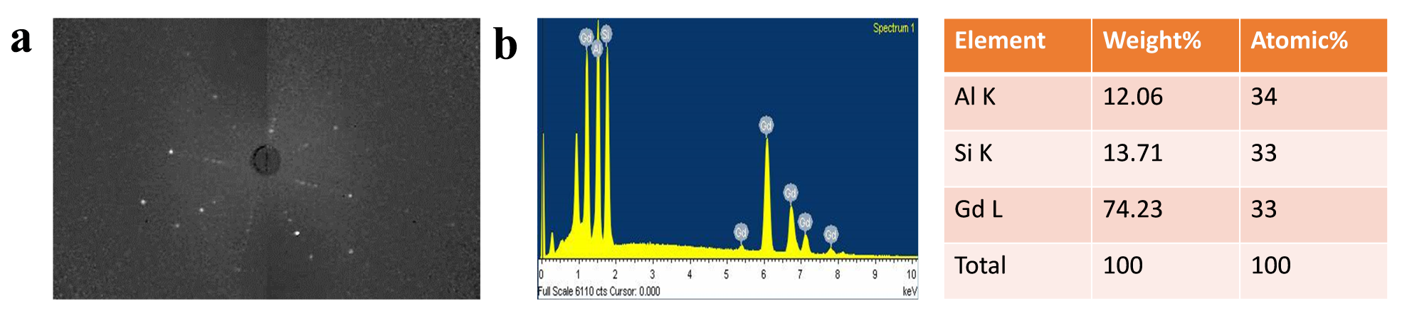
Multiple single crystals of GdAlSi were synthesized and carefully examined for elemental analysis. The rare-earth standards used in the analysis exhibited partial surface degradation, leading to a relatively broad range of total composition, approximately ranging from 97%-102%. However, despite this variation, the relative quantities of Al and Si were accurately determined. The resulting Al:Si ratios were found to be nearly 50:50 in all the samples. After conducting multiple compositional analysis, nearly 1:1:1 ratio of Gd:Al:Si were obtained by averaging the results, with normalization per rare-earth metal (see Fig. S1).
S1.2 Crystal Structure
Figure S2(a) shows the measured XRD-data along with the Rietveld refinement of GdAlSi, confirming the non-centrosymmetric nature of this compound, with the presence of broken crystal symmetry, similar to other RAlGe/Si systems. Laue pattern, as shown in Fig. S1(a)), confirms the high quality of the single crystal with tetragonal symmetry. The Rietveld refined atomic coordinates are presented in Table S1.
| Lattice parameters (Å) | Atom | Wyckoff position | Atomic coordinates | |||||
| Expt. | Optimized | |||||||
| 4.12 | 14.43 | 4.14 | 14.50 | |||||
| Al | 4a | 0.0 | 0.0 | 0.958(2) | ||||
| Gd | 4a | 0.0 | 0.0 | 0.374(2) | ||||
| Si | 4a | 0.0 | 0.0 | 0.793(2) | ||||
S1.3 Resistivity
Figure S2(b) displays the temperature-dependence of resistivity at two different magnetic fields. A distinct kink at/around 32 K confirms the antiferromagnetic (AFM) transition, which is consistent with previous magnetic and resistivity measurements [bobev2005ternary_sm].
S2 Ab-initio results
S2.1 Ground state magnetic structure
First principle calculations were performed on GdAlSi considering different magnetic configurations as shown in Fig. S3. Recently, NdAlSi has been shown to possess a commensurate ferrimagnetic (FiM) order [gaudet2021weyl_sm, li2023_sm] which has also been simulated here for GdAlSi. Among non-collinear configurations, a period-4 helical magnetic order with the magnetic moments oriented on the crystalline -plane has also been simulated. Both right-handed and left-handed helical magnetic order have been considered, denoted by “Helical ()” and “Helical ()” respectively. The simulated relative energies and Gd-projected moments for each configuration are summarized in Table S2. Out of all the configurations, AFM-I turns out to be the lowest in energy.
| Magnetic configuration | Relative total energy (meV) | Local magnetic moment on Gd atom () |
| AFM-I | 0 | 7.087 |
| AFM-II | 29 | 7.083 |
| AFM-III | 53 | 7.076 |
| AFM-IV | 137 | 7.057 |
| FiM | 82 | 7.068 |
| Helical () | 147 | 7.055 |
| Helical () | 147 | 7.055 |
| FM | 327 | 7.012 |
S2.2 Spin-polarized bulk Fermi surface
In the absence of spin-orbit coupling, the bulk Fermi surface (FS) of GdAlSi in the AFM-I configuration is spin-split which has been attributed to the presence of altermagnetism as discussed in detail in Sec. III(C) of main manuscript. The projection of the bulk FS on the plane is shown in Fig. S4. Interestingly, the bulk FS is not only spin-split but the spin up and spin down FS are rotated by 90∘ with respect to each other as a consequence of the opposite spin sublattice transformation .
| # | Cartesian coordinates of WPs | Type | Relative energy from (meV) | Chirality | ||
|---|---|---|---|---|---|---|
| (Å-1) | (Å-1) | (Å-1) | ||||
| 1 | 0.02334774 | 0.35268282 | -0.35921590 | IIA | 56.9 | -1 |
| 2 | 0.02318949 | 0.38668949 | 0.28815912 | IIB | 65.7 | -1 |
| 3 | -0.02309478 | 0.35207395 | 0.36053956 | IIA | 57.5 | 1 |
| 4 | -0.02274013 | 0.38723853 | -0.28827298 | IIB | 65.4 | 1 |
| 5 | 0.02329941 | -0.38638814 | -0.28817400 | IIB | 65.9 | 1 |
| 6 | -0.02298974 | -0.38670043 | 0.28832328 | IIB | 65.8 | -1 |
| 7 | -0.02311305 | -0.35136742 | -0.36132763 | IIA | 59.2 | -1 |
| 8 | 0.02321212 | -0.35188660 | 0.36053535 | IIA | 58.6 | 1 |
| 9 | 0.38648362 | -0.02303768 | -0.28842042 | IIB | 66.3 | -1 |
| 10 | 0.38635172 | 0.02314978 | 0.28840524 | IIB | 66.2 | 1 |
| 11 | 0.35245236 | -0.02311638 | 0.35944154 | IIA | 57.8 | -1 |
| 12 | 0.26287542 | -0.34160984 | -0.00323951 | IA | 24.8 | 1 |
| 13 | 0.26293202 | 0.34159153 | 0.00289293 | IA | 24.9 | -1 |
| 14 | 0.34155639 | 0.26296500 | 0.00269075 | IA | 24.9 | 1 |
| 15 | 0.26934249 | 0.42480217 | -0.00326708 | IB | 79.3 | -1 |
| 16 | 0.26945081 | -0.42471354 | 0.00316187 | IB | 79.5 | 1 |
| 17 | 0.35364172 | 0.02327349 | -0.35755327 | IIA | 55.6 | 1 |
| 18 | 0.34133130 | -0.26283603 | -0.00268189 | IA | 24.7 | -1 |
| 19 | -0.34141615 | -0.26279197 | 0.00290918 | IA | 24.8 | 1 |
| 20 | 0.42448142 | 0.26942807 | -0.00332700 | IB | 79.2 | 1 |
| 21 | 0.42441937 | -0.26945624 | 0.00333342 | IB | 79.0 | -1 |
| 22 | -0.42453955 | -0.26941235 | -0.00327385 | IB | 79.0 | 1 |
| 23 | -0.42460671 | 0.26936062 | 0.00325532 | IB | 79.3 | -1 |
| 24 | -0.38739632 | -0.02300432 | 0.28766724 | IIB | 65.5 | 1 |
| 25 | -0.38700553 | 0.02348663 | -0.28759203 | IIB | 65.9 | -1 |
| 26 | -0.34149597 | 0.26279987 | -0.00289444 | IA | 24.9 | -1 |
| 27 | -0.26947161 | -0.42432347 | -0.00337031 | IB | 79.4 | -1 |
| 28 | -0.35289234 | 0.02310173 | 0.35960125 | IIA | 56.6 | -1 |
| 29 | -0.35197737 | -0.02296815 | -0.36137773 | IIA | 58.3 | 1 |
| 30 | -0.26287467 | -0.34147170 | 0.00293753 | IA | 24.4 | -1 |
| 31 | -0.26947750 | 0.42445233 | 0.00343225 | IB | 79.4 | 1 |
| 32 | -0.26281726 | 0.34133262 | -0.00275370 | IA | 24.4 | 1 |
S2.3 Effect of spin-orbit coupling and bulk Weyl points
In Sec. III(C) of the main manuscript, we mentioned that incorporation of spin-orbit coupling (SOC) in the first principles calculation did not have much effect on the electronic band structure of GdAlSi. The electronic dispersion of GdAlSi with and without SOC for AFM-I magnetic configuration is shown in Fig. S5(a,b) respectively and for paramagnetic configuration (Gd -orbitals frozen in core) is shown in Fig. S5(c,d) respectively. Most notably, the spin-degeneracy along the direction is lifted due to SOC. But the spin degeneracy along remains intact which is a consequence of rotational symmetry in this system ( symmetry is contained in the little group of along ). The total magnetic moment of individual Gd atoms in this configuration remain equal in magnitude but parallel/antiparallel to the crytalline -axis. This is also seen if the spin components along the -axis (crystalline -axis), referred to as , is projected on the SOC band structure. The projected SOC band structure along with the total Berry curvature at the Fermi level is shown in Fig. S6. Since SOC perturbs the bands only slightly, the alternating nature of projections remain intact (see Fig. S6(a)) when compared with the spin-polarized band structure shown in Fig. S5. This alternating nature is further reflected in the total Berry curvature also (see Fig. S6(b)). Due to avoided crossings along the and paths, the bands along these two paths have equally large but opposite contributions to the total Berry curvature. This can lead to highly direction-dependent anomalous Hall and anomalous spin Hall effect in GdAlSi which can have practical applications in devices proposed in Sec. III(G) of the main manuscript.
Another consequence of SOC is the emergence of bulk Weyl points (WPs). The corresponding 3D bulk FS is shown in Fig. S7. The electron and hole pockets have been shown in red and blue respectively. More details about the location of bulk WPs in energy and -space are presented in Table S3. Figure S8(a) presents a symmetrized simulated Fermi surface, projected on the (001) surface of GdAlSi, along with the distribution of WPs. White arrows indicate the presence of short Fermi arcs that connect type-IA WPs, while also highlighting the extended Fermi arcs that connect the type-IB WPs (see main manuscript for details about type-IA and type-IB Weyl points). We have outlined the region of interest using a red dashed rectangle for the zoomed-in view for type-I Fermi arcs. Furthermore, we have emphasized the extended Fermi arcs that link the type-II WPs, which are found around the central pocket. The bulk band dispersion for both type-I and type-II WPs are shown in Fig. S8(b-e).
A close comparison with other non-magnetic and magnetic RAlX (X = Si,Ge) reveals certain interesting features about the surface Fermi arcs in GdAlSi. The four symmetrically placed butterfly-like bulk Fermi pockets along the direction are present in the surface Brillouin zone of all RAlX compounds studied till date [gaudet2021weyl_sm, li2023_sm, PhysRevLett.124.017202_sm, xu2017discovery_sm, Yang2020_sm, sanchez2020observation_sm]. These pockets contain projections of two pairs of WPs which reside on the plane in the bulk. One of the pairs (inner pair) is closer to the central pocket than the other (outer pair). The positive (black) and negative (white) chirality WPs within such a pair are mirror-symmetric along the surface high symmetry line and are expected to be connected via surface Fermi arcs. In non-magnetic RAlX such as LaAlGe [xu2017discovery_sm], the positive chirality WPs of the inner and outer pair are on the same side of the surface high symmetry line while the negative chirality WPs are on the opposite side. Both the inner and outer pairs are individually joined by short surface Fermi arcs crossing the surface high symmetry line. But for ferromagnetic RAlX such as PrAlGe [Yang2020_sm, sanchez2020observation_sm], the positive chirality WPs of the inner and outer pairs are on opposite sides of the surface high symmetry line. The same is true for the negative chirality WPs of both pairs. In this case, the surface Fermi arcs join opposite chirality WPs (one from inner and one from outer pair) on one side of the surface high symmetry line without crossing it. In the case of GdAlSi, the distribution of positive and negative chirality WPs is similar to the non-magnetic case and the surface Fermi arcs also cross the surface high symmetry line. But the inner pair (type-IA WPs) are joined by short Fermi arcs whereas the outer pair (type-IB WPs) are joined by extended Fermi arcs (even extending to the neigbouring surface Brillouin zone).
S3 ARPES results
S3.1 Surface Band Dispersion
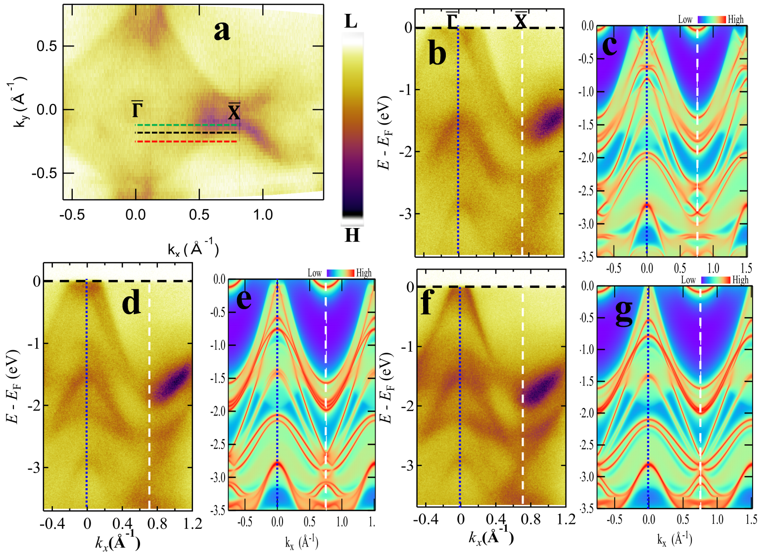
Figure S9 illustrates the Fermi surface of GdAlSi, showing a diamond-shaped structure featuring a symmetrical four-fold pattern along the (001) direction, measured using a photon energy of 50 eV. We study energy-momentum cuts of band dispersion taken at three distinct positions (cuts pass through the Fermi arcs as predicted by the calculated FS) aligned with - line. These positions are denoted by the green (lies on Å-1), black (lies on Å-1), and red (lies on Å-1) dashed lines as shown in Fig. S9(a). The corresponding ARPES band dispersion along the specified dashed lines (green, black, and red) are presented in Fig. S9(b, d, f), respectively. For a direct comparison, band structures computed along the same cuts are shown in Fig. S9(c, e, g), respectively. ARPES data reveal several interesting features, such as (i) pronounced linear band dispersion around in close proximity to , (ii) a strong, prominent band feature at -1.5 eV near the edge of the bulk-energy gap at (iii) two downward parabolic band dispersions at energies -1.5 eV and -2.5 eV, respectively near separated by the bulk energy gap (iv) A subtle downward parabolic-like band dispersion at -3.0 eV at .These significant features, particularly (i-iii), exhibit minimal variations in terms of energy and position across different energy-momentum cuts. The experimental data also clearly depict bulk energy gaps that align with the features in simulated band structure. This results in a good qualitative agreement between the experiment and theory.
S3.2 Fermi arc-like feature
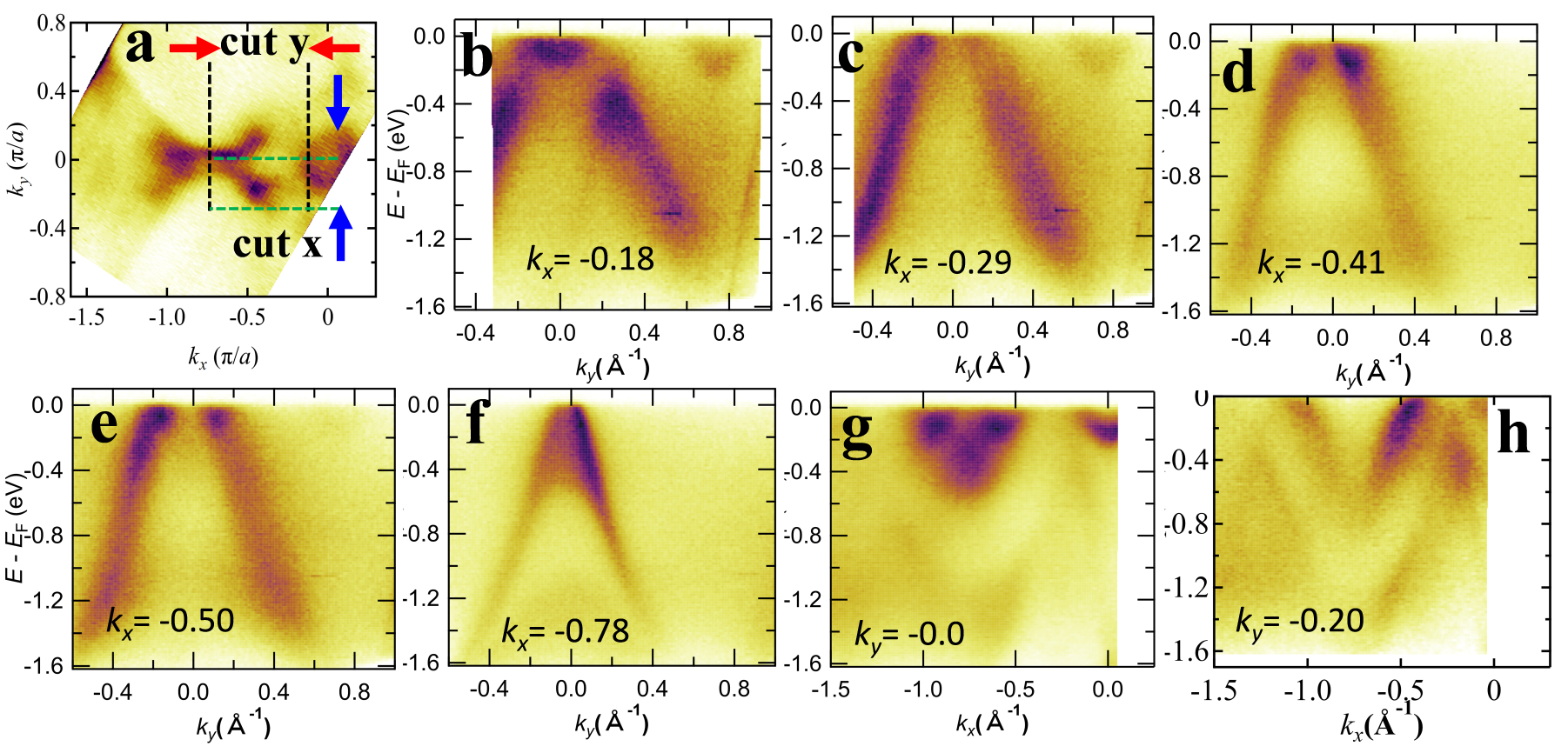
Our ab initio calculated Fermi surface indicates that type-II Fermi arcs are situated along the direction, while the type-I Fermi arcs are oriented along the direction as shown in the Fig. S8(a). To investigate the Fermi arc-like characteristics, we analyze energy-momentum cuts along both the horizontal and vertical directions to the line. Figures S10(b-f) present energy-momentum cuts along the line perpendicular to the path (cut y) at various positions, while Figs. S10(g-h) depict the horizontal cuts along the same path (cut x). The corresponding paths are shown in Fig. S10(a). ARPES measurements reveal mirror symmetric strong band dispersion features ( Å-1) around the electron pocket () for the cut y, as shown in Fig. S10(b). Mirror symmetric linear band dispersion features with negligible dispersion become more prominent for the cuts passing through type-I/II Fermi arcs as shown in Fig. S10(c-e). As observed in Fig. S10(d-e) along the cut y across the Fermi arcs (for Å-1 plane), two counter-propagating edge modes-like signatures are visible, which could be associated with opposite chiral charges (1). By comparing these experimental signatures obtained from the VUV ARPES results, with those of the predicted outcomes from our calculations, we offer an interpretation of the probable locations and existence of the predicted Weyl Fermions and potential Weyl Fermi arcs. Interestingly, a club-like feature with minimal dispersion is also observed in Fig. S10(g) for the cut x at .