Defect-driven tunable electronic and optical properties of two-dimensional silicon carbide
Abstract
Recently, an atomic-scale two-dimensional silicon carbide monolayer has been synthesized [Polley et al., Phys. Rev. Lett. 130, 076203 (2023)] which opens up new possibilities for developing next-generation electronic and optoelectronic devices. Our study predicts the pristine SiC monolayer to have an “indirect” band gap of 3.38 eV and a “direct” band gap of 3.43 eV calculated using the HSE06 functional. We performed a detailed investigation of the various possible defects (i.e., vacancies, foreign impurities, antisites, and their various combinations) on the structural stability, electronic, and optical properties of the SiC monolayer using a first-principles based density-functional theory (DFT) and molecular dynamics (MD) simulations. A number of physical quantities such as the formation energy, electronic band gap, and the effective masses of charge carriers, have been calculated. We report that the SiC monolayer has a very low formation energy of 0.57 eV and can be stabilized on TaC {111} film by performing the surface slab energy and interfacial adhesion energy calculations. Nitrogen doping is predicted to be the most favorable defect in silicon carbide monolayer due to its very low formation energy, indicating high thermodynamic stability. The analysis of the electronic band structure and the density of states shows that the additional impurity states are generated within the forbidden region in the presence of defects, leading to a significant reduction in the band gap. An interesting transition from semiconducting to metallic state is observed for and defective systems. For the pristine SiC monolayer, we find that the conduction band is nearly flat in the direction, leading to a high effective mass of . A significant red shift in the absorption edge, as well as the occurrence of additional absorption peaks due to the defects, have been observed in the lower energy range of the spectrum. The calculated absorption spectra span over the visible and ultraviolet regions in the presence of defects, indicating that the defective SiC monolayers can have potential optoelectronic applications in the UV-visible region.
I Introduction
The successful exfoliation of a graphene monolayer from graphite in 2004 [1] triggered a significant spike in the research activity of finding other possible two-dimensional (2D) materials. Due to their superior physical, chemical, and electronic properties [2, 3], 2D materials stand out as a new category when it comes to the possible commercial application [4, 5] in the manufacture of flexible electronic, nanoelectronic, and optoelectronic devices of the next generation [6, 7, 8, 9]. Their peculiar properties such as lower scattering rate of charge carriers, higher carrier mobility and conductivity [10, 11] make these materials more efficient than bulk silicon in the operation of electronic devices, which is the basis of the current semiconductor industry. However, the zero band gap of graphene [12] is the key issue which limits its potential application in nanoelectronics. Having a suitable band gap is essential for a 2D material to be a candidate for device applications. Therefore, many techniques have been employed to open the band gap of graphene, such as chemical doping, in-plane strain, functionalization with hydrogen, and molecule adsorption [13, 14, 15, 16, 17, 18, 19], etc.. Denis et al. [20] demonstrated that the band gap of monolayer and bilayer graphene can be opened with aluminum, silicon, phosphorus, and sulfur substitutional impurities. One approach to opening the band gap of graphene is to replace every second C atom with a Si atom. The resulting SiC monolayer has a stable planar structure with a band gap of 2.53 eV (using the generalized gradient approximation – Perdew-Burke-Ernzerhof functional, GGA-PBE), as reported in various density functional theory (DFT) based studies [21, 22]. The electronegativity difference between Si and C atoms causes polarization of the covalent bonds in the monolayer giving it a partly ionic character leading to the opening of the band gap. Also, the dynamical stability of the 2D-SiC monolayer has been confirmed in several previous reports [23, 24, 25]. A planar SiC monolayer sheet is formed due to the hybridization between Si and C atoms, as compared to the hybridization in bulk SiC phase [26, 27]. Theoretical studies have also confirmed that the ultrathin wurtzite structures such as SiC, BeO, GaN, ZnO, and AlN thin films can undergo phase transformation ( to ) and remain stable. Freeman et al. [28] demonstrated that wurtzite structures such as SiC and ZnO adopt a graphitic structure when thinned down to very few atomic layers, as it is the most stable structure for ultrathin materials. Later, this theoretical prediction was experimentally verified for ultrathin ZnO [29], AlN [30], and MgO films [31, 32]. Due to the phase transformation from bulk SiC to a single layer of SiC, the Si-C bond length is reduced from 1.89 Å to 1.79 Å, and the bond angle increases from 109° to 120° [33, 34, 27], consistent with its honeycomb structure. Due to the reduced dimensionality and quantum confinement along one direction, monolayer SiC is expected to exhibit exotic optical and electronic properties which may find potential application in the modern-day electronics industry [35, 36, 37]. As reported in the literature [38], the 2D-SiC has excellent mechanical properties and is found to be one of the stiffest 2D materials after graphene and h-BN. The SiC monolayer is highly suitable for its application in high-power and high-temperature devices due to its relatively wide band gap and superior physical and thermal properties [39].
In terms of experimental efforts, Lin and co-workers [40] were able to synthesize disordered quasi-2D-SiC flakes (thickness < 10 nm) through the reactive interaction between silicon quantum dots and graphene. Although these quasi-2D-SiC flakes were not atomically thin, the authors did observe changes in the electronic structure indicative of quantum confinement. Chabi et al. were able to push down the average thickness of 2D-SiC nanoflakes ( average size ) to 2-3 nm (which estimates between seven to ten atomic layers) by a catalyst-free carbothermal method [41]. Very recently, Polley et al. [42] reported to have successfully grown an atomically thin large-scale epitaxial monolayer of honeycomb SiC by employing the “bottom-up” solid state fabrication technique. They found that, unlike many other 2D materials that suffer environmental instability, this experimentally synthesized 2D-SiC monolayer is environmentally stable and does not degrade at room temperature.
It is well known that the defects (dopants, vacancies, antisites, interstitials, etc.) are unavoidable during fabrication or post-processing of materials. These defects play a crucial role in significantly tailoring the electronic and optical characteristics of the 2D material. Due to the quantum confinement effect of both host and defected wave functions in 2D materials, the impact of defects on the electronic and optical properties may considerably differ from their three-dimensional (3D) bulk counterpart. In this paper we undertake a systematic study of structural stability, electronic, and optical properties of some favorable defects in 2D-SiC monolayer utilizing first-principles-based DFT and MD simulations. We have investigated the point defects (i.e., vacancy, antisites), foreign impurity defects (i.e., boron, phosphorus, nitrogen and aluminum doping), and complex defects (i.e., doping-vacancy, antisite-vacancy), which are a combination of the aforementioned defects.
II Computational methods
All the calculations presented in this work have been performed within the framework of the first-principles DFT as implemented in the Vienna Ab initio Simulation Package (VASP) code [43, 44]. In this approach the electron-ion interactions are described using the projected augmented wave (PAW) [45] method with the energy cutoff set at 500 eV. The screened hybrid functional of Heyd–Scuseria–Ernzerhof (HSE06) [46, 47] with of the Hartree–Fock exchange and screening parameter has been employed for accurate band structure calculations. The Brillouin zone is sampled using the Monkhorst-Pack scheme, with an automatically generated k-point mesh of and for relaxation and single-point energy calculations, respectively. The convergence threshold for the forces felt by atoms is chosen to be 10-2 eV/Å, and for the total energy minimization, it is 10-5eV. For performing calculations on defective configurations, a supercell of SiC monolayer is chosen. A vacuum space of 15 Å is kept along the z-axis to eliminate the interactions between the periodic images of the supercell. The surface matching for the SiC monolayer and TaC {111} slab is performed using the Zur and McGill algorithm [48], which builds the lowest area supercell that matches the surface area of two lattices. In the slab and interface calculations, both lattice vectors and atomic positions are optimized. The van der Waals dispersion corrections are employed by using Grimme’s DFT-D3 method [49]. We have also considered dipole corrections in the calculation of the total energies of the surface slabs. The structural integrity at room temperature for the pristine as well as the defect-induced monolayer is verified by performing ab-initio molecular dynamics simulations (AIMD) [50]. The AIMD simulations are performed in two consecutive steps: First, the system is kept in a micro-canonical ensemble (NVE) for 6 ps of time duration using time steps of 1 fs each, while the temperature is raised from 0 to 300 K. Next, we kept the system in a canonical ensemble (NVT) at 300 K for 6 ps of time duration by employing a Nose–Hoover thermostat. For optical calculations, the frequency-dependent imaginary part of the dielectric function is obtained from the momentum matrix elements between the occupied valence bands and the unoccupied conduction bands, while the real part follows from Kramers-Kronig relations [51].
III Results and analysis
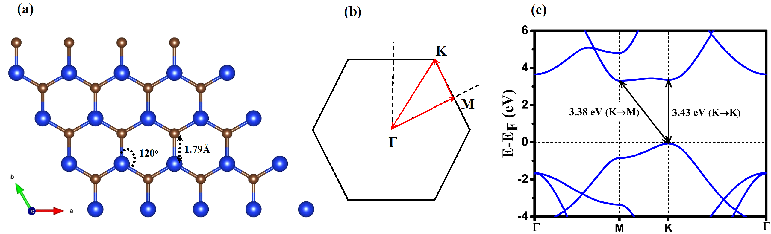
The valence shells of C and Si have electronic configurations of and , respectively. Thus, in the planar structure of the SiC monolayer, both the atoms participate in sp2–pz hybridization, so that the nearest-neighbor atoms (C and Si) are bonded together by bonds (Fig 1), while the pz orbitals of each atom give rise to the / bands corresponding to the valence/conduction bands of the system. Our calculations started by relaxing the pristine SiC monolayer, leading to the optimized bond length of 1.79 Å and optimized Si-C-Si (and C-Si-C) bond angle equal to 120° (Fig.1(a)), fully consistent with the previous theoretical studies [38, 33, 53, 27]. The nature of the band gap in SiC monolayer is debatable in the reported literature so far. The “direct” band gap has been predicted by Lin et al. [54] and Ferdous et al. [55] using SIESTA [56] and Quantum Espresso [57, 58] simulation codes, respectively, employing the GGA-PBE exchange-correlation functional. Guo et al. [22] and Hou et al. [cite-60] have also predicted a “direct” band gap for the SiC monolayer using the LDA and GGA-PW91 functional, respectively, as implemented in VASP. However, Hsueh and co-workers [24] reported that the band gap is “indirect” using the local density approximation (LDA) functional and transforms to “direct” upon employing GW self-energy corrections. Zheng et al. [62] have also claimed an “indirect” band gap using LDA and GWA functionals as implemented in the ABINIT code[63]. Ciraci et al. [38] also reported an “indirect” band gap based on their LDA calculations. It is commonly known that LDA/GGA functionals underestimate the band gaps in most materials. Therefore, to obtain a more accurate estimate of the band gap of the SiC monolayer, we decided to perform calculations using the hybrid functional HSE06. For this purpose, we used the geometry optimized using the PBE functional, and performed HSE06-based band structure calculations on the primitive cell of SiC monolayer containing two atoms. We found an “indirect” band gap of 3.38 eV and a “direct” band gap of 3.43 eV in the SiC monolayer, as demonstrated in Fig. 1(c). For the sake of comparison, we have also computed the band structure using the PBE functional (see Fig. S1 [64]), and found that the system exhibits an indirect band gap of 2.55 eV and a direct one of 2.56 eV . Upon comparing the two band structures, we conclude that they differ quantitatively with the HSE06 band gaps, being 0.8 eV larger; however, their qualitative features are very similar.
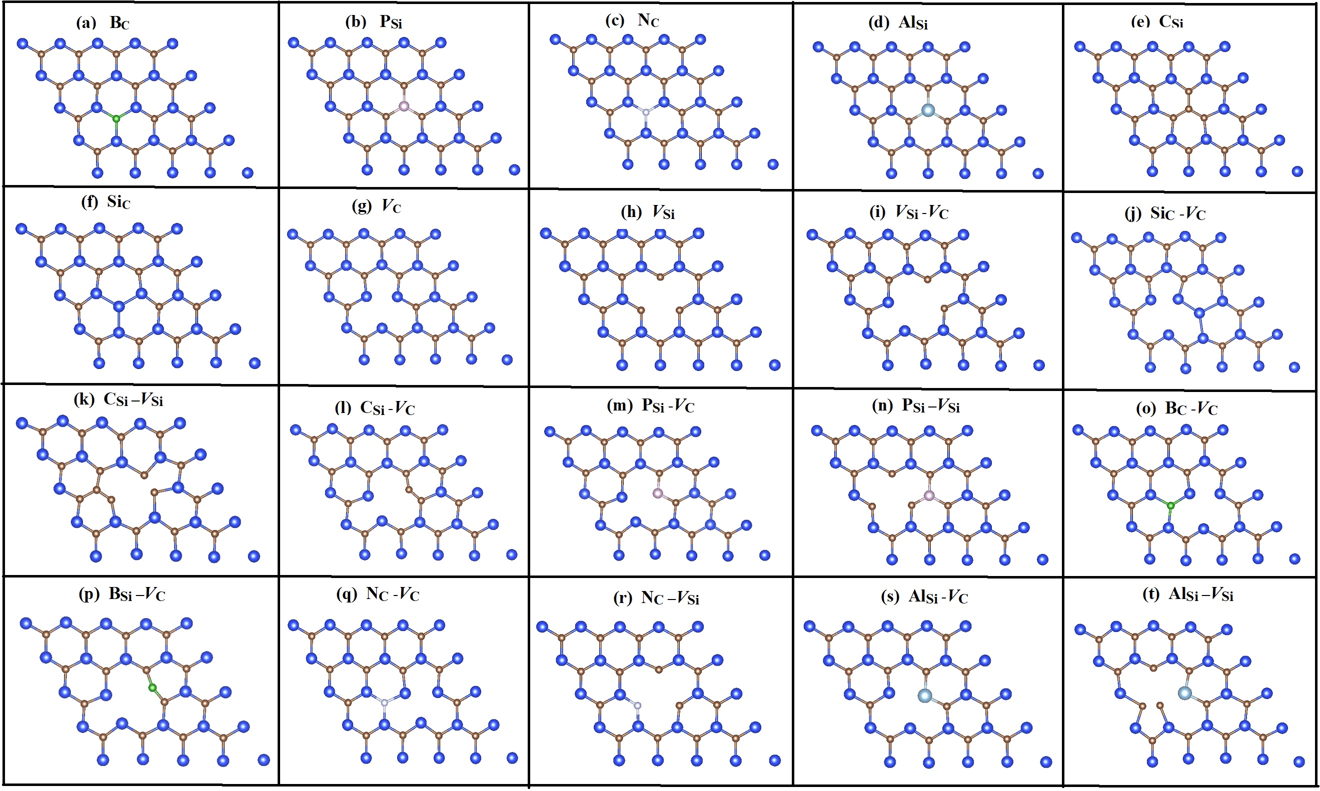
Due to the slight difference in the relative energies in the conduction band edge at the K and M points of the Brillouin zone, the nature of the band gap and the related properties can be easily tuned with the introduction of various types of defects, impurities, strains, etc.. Hassanzada et al. [65] proposed that the Stone-Wales-related defects could be promising hosts for single-photon quantum emitters. The paramagnetic color centers are connected to silicon vacancy-related defects, as reported by Mohseni and co-workers [33]. The effects of various substitutional impurities, adatoms, and vacancy defects on magnetic properties have been investigated by Ciraci et al. [66]. Despite a fair number of studies on 2D-SiC monolayer, a comprehensive study of the stability of various defective structures and their electronic and optical characteristics is still lacking. Therefore, we present here a detailed investigation of the structural stability and optoelectronic properties of SiC monolayer with following types of defects: (i) substitutional defects, where a dopant X can replace one Si atom or a dopant Y can replace one C atom, i.e. or , (ii) vacancy, where either a Si or C atom or both the atoms are missing from their respective sites i.e. or or -, (iii) antisites, where a Si atom is present at the C atom site or vice-versa i.e. or , (iv) antisite-vacancy, a combination of both (ii) and (iii), where either a C or Si atom is missing from their respective sites forming a vacancy defect, while at the same time, C atom is present at the Si-site or vice-versa, i.e., - or -; and (v) doping-vacancy, a combination of both (i) and (ii), i.e., - or -. The ground state geometries of these defects in a 44 supercell of SiC monolayer are presented in Fig 2.
We have divided the remainder of this section into four parts to discuss the effects of defects on (a) structural stability, (b) electronic structure, (c) effective mass of charge carriers, and (d) optical properties.
III.1 Stability of defects in 2D-SiC monolayer: Ab Initio Atomistic Thermodynamics and Molecular Dynamics calculations
In this section, we first probe the thermodynamics of various defect-induced SiC monolayer systems by calculating their formation energies in both Si-rich and C-rich environments, which is crucial in supporting the experimental work to improve the setup conditions during the growth of the 2D-SiC monolayer. The structural stability of the defective systems is probed by performing AIMD simulations at room temperature.
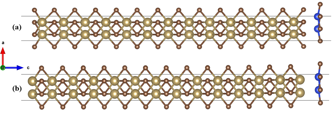
The formation energy of monolayer SiC is obtained using the formula = , where is the chemical potential of the monolayer SiC unit cell, while denote the chemical potential of the stable phase of Si (C). The calculated formation energy of the monolayer is found to be 0.57 eV, which is in excellent agreement with the values reported in the literature [65]. The low positive value of formation energy indicates that the SiC monolayer is a metastable phase of silicon carbide and hence could be stabilized experimentally. To investigate the role of substrate in the growth of SiC monolayer, we have performed substrate-film adhesion energy calculations using the first-principles DFT, combined with the substrate interface theory. Experimentally, an epitaxial monolayer of 2D SiC was recently synthesized on ultrathin rocksalt cubic TaC{111} surface of thickness 3nm, which was accommodated on a 4H-SiC substrate [42]. We have extracted a 3.3 nm thick {111} Miller surface of rocksalt cubic TaC from the bulk TaC cubic halite, and performed the full geometry optimization and self-consistent field calculations. The surface slab energies of TaC{111} slab and SiC monolayer are calculated using the Eq. (1) [cite-67, cite-68].
| (1) |
where and are the total energies of the surface slab and bulk units, , , , and are, respectively, the number of formula units, number of extra atoms in surface slab, surface area, and chemical potential of elementary atoms. , , and are calculated from their stable bulk phases under both Ta-rich and C-rich conditions, since the monolayer SiC is grown on the TaC film. The surface energy of monolayer SiC is found to be 11.55 , computed with respect to the stable 4H phase of SiC. The surface energies of the 3.3 nm thick TaC {111} slab with C and Ta-terminations are provided in Table 1. We found that Ta-terminated TaC{111} slabs have lower surface energy compared to C-terminated TaC{111}, which is consistent with the previous slab energy calculations of various rocksalt transition-metal carbide facets by Quesne et al.[69]. Next, we construct two interfaces of TaC {111} slab and SiC monolayer corresponding to the C and Ta terminations of TaC. The silicon carbide monolayer is kept at a distance 2 Å above the metal carbide’s surface, and the optimized distance between the C(Ta) terminated TaC {111} and Si atom of monolayer SiC is 2.36 Å (2.72 Å). The optimized structures of the TaC {111}-SiC interface, with the C and Ta terminations are presented in Figs. 3(a) and 3(b). We report a small lattice mismatch of 1.87 % in the interface structures composed of TaC {111} 3.3 nm thick film and SiC monolayer. Next, we calculate the bonding strengths of the atoms present at the TaC {111}-SiC interface and the interface stability by calculating the interfacial adhesion energy using Eq. (2)[70]
| (2) |
Here, , , and are the total energies of the SiC monolayer, TaC{111} slabs, and TaC{111}-SiC interfaces, respectively, and is the lateral interface area. The adhesion energy for the TaC {111}-SiC monolayer was found to be -1.44 and -2.05 for C and Ta-terminated TaC {111} facets. The negative values of adhesion energies imply that TaC {111} substrate can stabilize the SiC monolayer. The adhesive energy of the Ta-terminated TaC {111}-SiC interface is less than that of the C-terminated TaC {111}-SiC interface, because Ta-terminated TaC {111} facet is more stable than the C-terminated TaC {111}.
| Ta-termination | C-termination | Ta-termination | C-termination | ||
|---|---|---|---|---|---|
| C-rich | Ta-rich | C-rich | Ta-rich | ||
| 3.10 | 1.98 | 5.26 | 6.34 | -2.05 | -1.44 |
The cohesive energy of an isolated pristine SiC monolayer is calculated as in terms of the optimized total energy of the unit cell of SiC monolayer and total energies of isolated Si and C atoms, respectively. The calculated cohesive energy is found to be -11.87 eV, indicating the high stability of the material.
We investigated the relative stability of various possible defects under investigation by computing their formation energies. The formation energy of a neutral defect, is calculated using Eq. (3) [71, 72].
| (3) |
Above and represent the total energies of the optimized structures of the defective, and pristine monolayers, respectively. is the number of atoms removed from ( or added to () the SiC monolayer to form a defect, and is their corresponding chemical potential. The chemical potential, depends on the chemical environment of the system, therefore we have calculated the formation energies of defects in both Si-rich (C-poor) and C-rich (Si-poor) growth conditions. of the constituent atoms are calculated from their stable bulk phases. The calculated formation energies of various possible defective systems considered in this work are shown in Fig. 4 for both Si-rich (C-poor) and C-rich (Si-poor) growth conditions.
Here, the formation energy is calculated using the finite-size supercell methodology, where a defect is introduced in a suitably large simulation supercell to minimize the defect-defect interaction, which can have a significant impact on the defect formation energy. For charged defects, the interactions between the periodic images of defects are significant due to the presence of long-range electrostatic potential term that converges very slowly as a function of supercell size. However, for neutral defects, which are explored in this work, the defect-defect interactions are negligible. Therefore the formation energy converges fairly quickly with the increasing supercell size. As a result, the simulations employing smaller supercells can yield fairly precise estimates for the formation energy of the neutral defects. In this work, we have computed the defect formation energy using a (4 × 4) supercell and also compared it with the formation energy obtained using different supercell sizes, i.e., (3 × 3), (5 × 5) and (6 × 6) (Fig. 4). We found that the trend in the formation energy of various defects considered in the present study remains unaffected by the different supercell sizes (Fig. 4). Additionally, the formation energy is very well converged for the majority of the defects which makes the (4 × 4) supercell size a suitable choice to further study the defect properties.
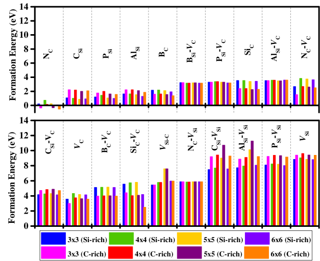
The calculated theoretical formation energy of the defect is the lowest for the C-rich growth condition, indicating that this defect is most likely to be found in the SiC monolayer. The defect formation energy of is lower than that of , which is similar to the case corresponding to the bulk 4H-SiC phase [73]. The formation energies of -, -, -, and - are greater than those of -, -, -, and - . The large formation energies associated with the Si vacancy are expected, because the Si-atom is heavier than the C-atom, and hence will be difficult to remove. Another point that can be noted is that the formation energy of the type defect is lower than the type defect because C atoms prefer the sp2 configuration more than the Si atom does. Among the dopant-type defects, and have greater formation energies than and , which can be attributed to the atomic size and electronegativity of the dopant atoms. To further reveal the thermal stability of pristine and defective systems at room temperature (300 K), we performed ab-initio molecular dynamics (AIMD) simulations. The maximum bond length variation is found to be around for a pristine SiC monolayer, which is not significant and corresponds to only 0.08 Å. It has been observed that for the doped, antisite, vacancy and complex defect cases, the maximum bond length fluctuations are and for , , , and - defects, respectively. Thus, we conclude that both the pristine as well as defective SiC monolayers are stable at room temperature.
III.2 The influence of defects on the electronic structure and magnetic properties
This section is devoted to the analysis of the electronic band structure and electronic density of states (DOS) of various structures under investigation. As a benchmark test for comparison, we first investigated the electronic band structure of a 4 × 4 supercell of the pristine SiC monolayer. Notably, more bands populate the Brillouin zone because of the band folding caused by a larger number of atoms in the supercell as compared to the primitive cell. We also examined the spin-polarized atom-projected electronic density of states (PDOS) to explore the contribution of each atom and orbital to the valence and conduction bands in the proximity of the Fermi level. The p-orbital of the C-atom clearly dominates the valence band, whereas the Si atom’s p-orbital mostly contributes to the conduction band as seen in Fig. 5(b).

To elucidate the role of defects on the electronic structure of defected 2D-SiC, we have performed band structure and PDOS calculations using hybrid HSE06 functional (refer to Figs. 6 and 7). It is interesting to note that the additional defect states are generated near the Fermi level for and type defects as compared to the pristine monolayer [see Figs. 6(a) and 6(b)]. This leads to a significant reduction in the band gap , which becomes 1.15 eV for and 0.90 eV for , respectively. The strong peak of the p-orbital of the dopant atom, i.e., B (P), is observed near the Fermi level for defected systems as shown in Figs. 7(a) and 7(b), which confirms that these additional states in the band structure are arising due to the dopant atom.
However, for defects, as shown in Figs. 6(c)– 6(d) (band structure) and Figs. 7(c)–7(d) (PDOS), the Fermi level lies near the bottom (top) of the conduction (valence) band within the continuous density of states and hence shows the interesting defect-induced transition from the semiconducting to metallic state. The metallicity is basically due to the shift of the Fermi level of the supercell caused by an extra valence electron in case of and one less electron in case as compared to the pristine supercell. From Figs. 7(c) and 7(d) it is obvious that the dominant contribution to the PDOS near the Fermi level is due to the p orbital of the Si (C) atom for defects.
For the antisite defects, i.e., and defects, only one defect state corresponding to the p orbital of C and Si, respectively, is found in the midgap region [see Figs. 6(e), 6(f) and 7(e), 7(f)]. Therefore, the system is expected to behave as n-type (p-type) semiconductor under the presence of () defects with the reduced band gap of 2.66 eV (2.58 eV).
In the case of a single C (Si)-atom vacancy, i.e., , the atoms nearest to the vacancy defect have an unpaired electron that forms an unsaturated covalent bond and causes the impurity bands to emerge in the forbidden region exhibiting a band gap of 1.40 eV (0.34 eV) [see Figs. 6(g) and 6(h)]. A detailed examination from PDOS [Figs. 7(g) and 7(h)] clearly demonstrates that the p orbital of Si (C) atoms for type defect are the primary cause of the impurity states. The result contrasts with the bulk 4H-SiC phase [73], where impurity states created due to a single Si or C atom vacancy cross the Fermi level, inducing the metallicity in the system. The mid-gap defect states are also observed in the electronic structure of the - double vacancy, mainly due to the p orbital of the C atom, as is obvious from Figs. 6(i) and 7(i). This leads to the reduced band gap of 1.90 eV.
The symmetric character of PDOS suggests the non-magnetic nature of the pristine SiC monolayer [Fig. 5(b)]. However, some defects can induce a net magnetic moment due to imbalanced up and down spin channels, as observed in Fig. 6. For BC, PSi, and NC defects, the total magnetic moment induced in the defective system is , , and , respectively (refer to Table 2), while for , and defects the system remains non-magnetic, which is consistent with the results reported by Bekaroglu et al. [66]. In the case of single defects, i.e., VC and VSi, the magnetic moment is comparatively higher, which is , and , respectively. In Table 2, we have listed the resulting net magnetic moment corresponding to various defective systems.
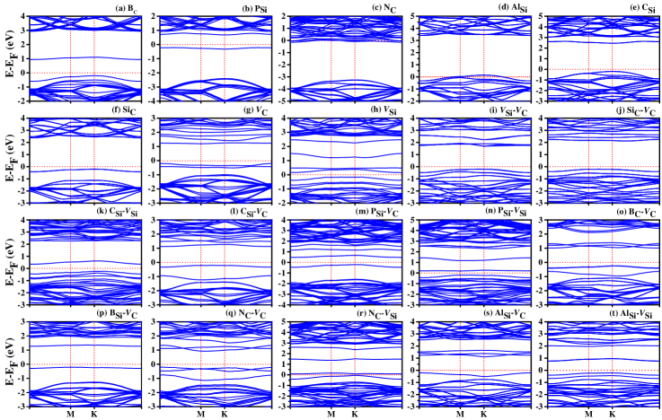
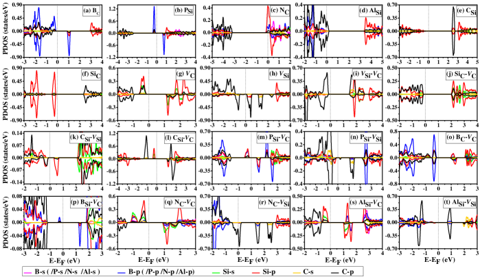
The complex defects (i.e., antisite-vacancy and dopant-vacancy) have a qualitative impact on the electronic structure of the system. The PDOS curve for the - defect indicates that the defect states hybridize with the valence and conduction bands in the system [see Fig.7 (j)], leading to a reduced band gap of 2.34 eV, while the defect states near the Fermi level for - and - [see Figs. 7(k) and 7(l)] arise mainly due to the p orbitals of the Si and C atoms, resulting in a smaller band gap value of 0.59 and 1.34 eV, respectively. An overlapping is observed between the p orbital of P and Si atoms for the - defect, which indicates a strong hybridization between them. The additional impurity states due to the p orbital of the B atom are observed for - and - defects, as shown in Figs. 6(o) and 6(p), resulting in a significant reduction in band gap to 1.26 and 1.49 eV, respectively. For - and - , the defect states arise mainly due to the p orbitals of the Si atoms, with a very small contribution from the p orbitals of the C atom, as is evident from Figs. 7(q) and 7(s). The additional impurity electronic states due to the p orbital of the C atom dominate on both sides of the Fermi level for -, - and - type defects [see Figs. 7(n), 7(r) and 7(t)] with a reduced band gap value of 0.39, 0.14, and 0.98 eV, respectively. For all the cases of complex defects considered in this article, the semiconducting nature of the material remains intact.
We observed an interesting nonmetal-to-metal transition for and defects. It is important to investigate if the metallic nature of and defective systems is sustained under different defect densities. Therefore we have performed density-of-states calculations employing the HSE06 functional using different supercell sizes, i.e., (3 × 3), (5 × 5), and (6 × 6), and compared the results with a (4 × 4) supercell. For the defect, the Fermi level crosses the conduction (valence) band for all supercell sizes, indicating the metallic nature of these materials remains intact in the relatively dense and dilute limits of such defects. We found that the conduction and valence band edges for and defects are adequately converged with different supercell sizes, as shown in Fig. S2 [64], implying a (4 × 4) supercell is an appropriate choice to study such defects in the SiC monolayer.
III.3 Effective mass of charge carriers
The effective masses of electrons and holes in semiconductors are important because they determine the mobilities of the charge carriers, subsequently influencing their photoelectric and thermoelectric properties [74]. In this section we present our results on the effective masses of charge carriers because, to the best of our knowledge, no such prior calculations on the pristine and defective SiC monolayers exist. We have computed the effective mass of electrons and holes using the parabolic approximation around the band extremas according to Eq. (4) [75]:
| (4) |
where is the rest mass of the electron, is the reduced Planck constant, is a wave vector in the first Brillouin zone, is the corresponding Kohn-Sham eigenvalue, and denotes the location of the band extremum. The calculated value of electron and hole effective masses for pristine SiC monolayer at its band extrema, i.e., and , are found to be and , respectively. However, interestingly, it can be noticed that the electron effective mass along the high-symmetry directions, i.e., and , are found to be and , respectively. This is due to the decrease in the band dispersion along the direction, which results in a higher effective mass. Furthermore, the hole effective mass is found to be and , respectively. These results suggest that the charge carriers are more mobile along the direction as compared to the direction.
| Defect-induced system | Electron effective mass | Hole effective mass | Total magnetic moment |
|---|---|---|---|
| Pristine-SiC-monolayer | |||
| BC | |||
| PSi | |||
| NC | |||
| AlSi | |||
| CSi | |||
| SiC | |||
| VC | |||
| VSi | |||
| VSi-VC | |||
| SiC-VC | |||
| CSi-VSi | |||
| CSi-VC | |||
| PSi-VC | |||
| PSi-VSi | |||
| BC-VC | |||
| BSi-VC | |||
| NC-VC | |||
| NC-VSi | |||
| AlSi-VC | |||
| AlSi-VSi |
To understand the influence of defects on the mobilities of charge carriers, we have carried out the effective mass calculation for the defected systems as well. The calculated values of the electron and hole effective masses at the band extremas for the pristine, as well as various defected systems under the scope of this work, are listed in Table 2. For defective systems, the electron and hole effective masses of and respectively, were obtained at the conduction (valence) band extrema. For the defect case, the electron effective mass is calculated to be while the hole effective mass is found to be The electron effective mass for double vacancy is , which is substantially lower than the value of the single vacancy defect. On the other hand, the value of the hole effective mass for the - defect is higher than that of the defect . Exceptionally low electron effective mass values of and are obtained for the - and - defects, respectively, which are comparable to the bulk silicon electron effective mass, estimated to be [76, 77]. A low effective mass leads to a pronounced carrier transport property, indicating the high potential of such materials in photovoltaic applications [78, 79]. For the double defects CSi-VC, PSi-VC, and BSi-VC, the electron effective masses are much higher than , suggesting their applications in thermoelectric devices aimed at converting otherwise wasted heat into electric power [80].
III.4 Influence of defects on the optical properties
In this section we present and discuss our results on the optical absorption spectra of the pristine and defective SiC monolayers with the aim of understanding the influence of defects on their optical properties. Our findings give insights into the rich electronic and optical properties of this newly synthesized SiC monolayer for its potential application in electronic and optoelectronic devices of the next generation. For this purpose we have computed the frequency-dependent real and imaginary part of the dielectric functions using the orbitals and the band structures obtained from the GGA-PBE calculations. The imaginary part was computed by performing the sum over the conduction-band states, while the real part was obtained from the imaginary part using the Kramers–Kronig (KK) relationship. Thus, these calculations were performed within the independent-electron model, ignoring the excitonic effects that arise due to the electron-hole interactions. To include the influence of excitonic effects, one must perform calculations using approaches such as the time-dependent density-functional theory (TDDFT) or the Bethe-Salpeter equation (BSE) that take into account the quantum many-particle effects. However, the purpose behind the present calculations is to obtain a semiquantitative understanding of the influence of defects on the optical properties, for which we feel that the independent-electron approach is sufficient. The following equations (5 and 6) are used to compute the relevant refractive index and optical absorption of the system with respect to the photon energy.
| (5) |
| (6) |
For the pristine SiC monolayer, absorption starts at around 2.23 eV, with its first absorption peak at 2.87 eV, followed by a second absorption peak at 3.41 eV for the light polarized in the plane (-polarized), i.e., with the electric field of the radiation or directions [8(c)]. We also note that for the -polarized light, the optical response of the pristine monolayer is fully isotropic, i.e., the same for both and polarization directions. While for the -polarized light ( , or -polarized), the absorption starts at a higher energy of 4.30 eV, followed by the first absorption peak at 4.81 eV, which is expected for two-dimensional materials since more energy is required to excite electrons in a direction perpendicular to the plane of the material because of the stronger confinement in that direction. Several other peaks are located in the ultraviolet region of the spectrum, indicating a number of transitions from the valence band to the conduction band. The dominant peak corresponding to the maximum absorption is observed at 8.09 eV (-polarized) and 10.41 eV ( -polarized). Table 3 shows the first and the most intense absorption peak values for the pristine SiC monolayer and the bands that contribute to the single electron transition corresponding to the peak. In order to determine the conduction bands involved in these transitions, we compared the excitation energies of the first and the most intense peaks of the absorption spectra with the energy difference between highest valence band and the conduction band , calculated using the PBE-GGA band structures [see Fig. S3 [64]].
We found that the transition occurs at the point for the first and most intense peaks for the -polarized light, while the transition is at K and points, respectively, for the first, and the most intense peaks in case of -polarized light.
| Peak | Peak locations (eV) | |
|---|---|---|
| -polarized | -polarized | |
| First peak | 2.87 | 4.81 |
| Most intense peak | 8.09 | 10.41 |

The static dielectric constant and the refractive index are found to be 3.85 (1.93) and 1.96 (1.39) for -polarized (-polarized) light, as shown in Figs. 8(a) and 8(b). For the photon energy ranges 3.6-5.6 eV and 8.1 eV and higher for the -polarized light, the refractive index () of SiC monolayer is found to be less than that of the glass (), indicating comparatively higher transmission and hence low absorption. While for the-polarized light, higher transmission will be observed for the energy range 0.0-4.3 eV.
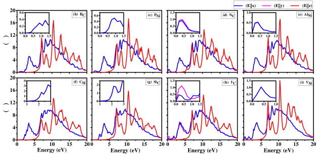
As can be seen from calculated optical absorption data (Figs. 9 and 10), the optical absorption for the defective SiC monolayers starts at much lower energies, as compared to the pristine one. The reason behind the onset of absorption at lower energies in the defective systems is the presence of defect levels in the midgap region that effectively reduce the optical gap in these materials. For the -polarized light, the absorption starts at around 0.36 eV for and defects due to the additional impurity states generated above and below the Fermi level. The first absorption peak is observed in the infrared (IR) region of the spectrum at 0.89 eV and 0.74 eV for and defects, respectively. For and , the defect states appear at the Fermi level (Fig. 7) and hence the absorption starts at 0 eV, indicative of the metallic nature of these systems. The first peak is found at 0.20 eV for and defects. Similarly, due to the impurity states being very close to the Fermi level, the onset of absorption starts again near zero photon energy for and defects, with the first absorption peak at 0.17 and 0.38 eV, respectively. A number of defect states appear above and below the Fermi level, which leads to more than one absorption peak within a small energy interval in the infrared region of the spectrum. It could be noted that a slight anisotropy in the optical absorption in the xx and yy direction is observed for the defect. For the cases of and , the defect states appear close to CBM and VBM, respectively. Thus the absorption spectrum does not change significantly as compared to the pristine monolayer, with the first absorption peaks at 2.24 and 2.17 eV, respectively. Furthermore, no significant changes are observed in the optical absorption spectrum for the -polarized light for the systems with simple defects as compared to the pristine monolayer.
Next we discuss the absorption spectra of monolayers with complex defects. For the -polarized light, the absorption starts at around 1.17 eV leading to the first absorption peak at 1.63 eV for the - defect. For -, -, and - defects, the absorption starts near 0 eV, owing to their very low band gap. Their first absorption peak is observed at 0.40, 0.36, and 0.54 eV, respectively. The absorption spectra of the - defect is similar to the pristine case with the first absorption peak shifted to 2.67 eV. A sharp absorption peak occurs at 1.13 and 1.10 eV for - and - defects. Broad absorption peaks at 1.44, 1.72, and 0.18 eV corresponding to -, -, and - defects, respectively, indicate several electronic transitions from occupied energy states to unoccupied energy states within that energy interval. - and - have new absorption peaks at 1.99 and 0.54 eV, respectively, while the second absorption peak splits into more than one peak, indicating multiple transitions. Notably, a small anisotropy in the optical absorption is observed for the -polarized light with respect to and polarization directions for all the complex defects under consideration. For the -polarized light, no additional absorption peaks or shift of absorption peaks is observed, except that a significant decrease (0.54 times) in the peak strength is noticed for the - defect.
As is known, materials which show absorption in the visible region are suitable for photocatalysis using sunlight. Thus these defective systems can be utilized for photocatalysis. Several defective systems showed absorption peaks in the infrared (IR) region of the spectrum, which makes them crucial for the rational design of IR LEDs for their application in sensing, communication devices, remote control, etc. The optical absorption spectra of defective systems also cover a wide range of visible and UV regions, indicating that these materials can have important applications in optoelectronic devices in a broad frequency range.

IV CONCLUSION
In this paper we presented a systematic and detailed first-principles DFT-based study of the stability, electronic structure, and optical properties of both pristine and defective SiC monolayers. A variety of single as well as double atom defects were considered employing supercells, and their influence on a number of properties, such as the band gap, effective electron and hole masses, and optical absorption spectra, were studied. The negative adhesion energy of SiC monolayer on C and Ta-terminated TaC {111} film indicates that SiC monolayer can be stabilized upon metal carbide film. Furthermore, by calculating the formation energies of all the defective configurations, within both the Si and C rich conditions, we demonstrated that the defective structures can be easily synthesized.
To summarize, we found that the electronic structure and optical properties of the SiC monolayer can be tuned in a variety of ways by introducing defects in a controlled manner. Analyzing the calculated theoretical formation energies of various defects, we predict that defect could be naturally present in silicon carbide monolayer even during growth due to its very low formation energy. The formation energy related to Si-vacancy defects is found to be higher as compared to C-vacancy-related defects. This behavior is expected since the Si-atom has a greater atomic mass than the C-atom and will be difficult to remove. We also verified that the trend in formation energy remains the same with different defect concentrations. The structural solidity at room temperature for defected systems has been verified by employing ab-intio molecular dynamics (AIMD) simulations. The in-depth analysis of the electronic band structures and the atom projected density of states (PDOS) showed that the additional impurity states are generated within the forbidden region of pristine silicon carbide in the presence of defects. These impurity states lead to the dramatic reduction in the band gap, which can improve the electrical conductivity of the material. An interesting transition from semiconducting to metallic is observed for and defective systems. Furthermore, we also calculated the electron and hole effective masses, which is one of the fundamental characteristics of the semiconductor. We observed that the electron effective mass for pristine silicon carbide monolayer is significantly higher along the direction, which will lead to better thermoelectric performance. Interestingly, the electron effective mass at the band extrema for - and - defects is found to be very low, which is comparable to the bulk silicon effective mass. Such low-effective mass materials are suitable for high-speed electronic devices. The real and imaginary parts of the frequency-dependent dielectric function have been used to calculate the refractive index and optical absorption coefficient. In terms of the onset of optical absorption, both the pristine and defective monolayers exhibit significant anisotropy with respect to the light polarized parallel to the plane of the monolayer as compared to the perpendicularly-polarized light. This can be seen as a structural fingerprint in the optical response, which can be used for the detection of the monolayers employing optical spectroscopy. Further, it has been found that the absorption edge shifts towards the lower energy range of the spectrum for defect-induced systems as compared to its pristine counterpart. The additional absorption peak is observed at 0.89 eV and 0.74 eV for and defects (-polarized light), respectively. While for and defects, the first absorption peak shifts to 2.24 and 2.17 eV (-polarized light), respectively, since the defect states are generated very close to the conduction band and valence band, respectively. Therefore, these nanosystems exhibit excellent ability of optical absorption in the near-infrared and visible regions of the spectrum, making them viable for future photovoltaic and optical devices. Our results will help to speed up the understanding of defects in 2D SiC monolayer to be realized experimentally in the near future.
References
- Geim and Novoselov [2007] A. K. Geim and K. S. Novoselov, Nature materials 6, 183 (2007).
- Partoens and Peeters [2006] B. Partoens and F. M. Peeters, Phys. Rev. B 74, 075404 (2006).
- Bostwick et al. [2009] A. Bostwick, J. McChesney, T. Ohta, E. Rotenberg, T. Seyller, and K. Horn, Progress in Surface Science 84, 380 (2009).
- Hicks and Dresselhaus [1993] L. D. Hicks and M. S. Dresselhaus, Physical Review B 47, 12727 (1993).
- Liu and Zhou [2019] B. Liu and K. Zhou, Progress in Materials Science 100, 99 (2019).
- Wang et al. [2012] Q. H. Wang, K. Kalantar-Zadeh, A. Kis, J. N. Coleman, and M. S. Strano, Nature nanotechnology 7, 699 (2012).
- Mak and Shan [2016] K. F. Mak and J. Shan, Nature Photonics 10, 216 (2016).
- Zeng et al. [2012] H. Zeng, J. Dai, W. Yao, D. Xiao, and X. Cui, Nature nanotechnology 7, 490 (2012).
- Schedin et al. [2007] F. Schedin, A. K. Geim, S. V. Morozov, E. W. Hill, P. Blake, M. I. Katsnelson, and K. S. Novoselov, Nature materials 6, 652 (2007).
- Morozov et al. [2008] S. V. Morozov, K. S. Novoselov, M. I. Katsnelson, F. Schedin, D. C. Elias, J. A. Jaszczak, and A. K. Geim, Phys. Rev. Lett. 100, 016602 (2008).
- Ferrari et al. [2006] A. C. Ferrari, J. C. Meyer, V. Scardaci, C. Casiraghi, M. Lazzeri, F. Mauri, S. Piscanec, D. Jiang, K. S. Novoselov, S. Roth, and A. K. Geim, Phys. Rev. Lett. 97, 187401 (2006).
- Novoselov et al. [2005] K. S. Novoselov, A. K. Geim, S. V. Morozov, D. Jiang, M. I. Katsnelson, I. V. Grigorieva, S. Dubonos, and a. Firsov, nature 438, 197 (2005).
- Boukhvalov and Katsnelson [2008] D. Boukhvalov and M. Katsnelson, Physical Review B 78, 085413 (2008).
- Cocco et al. [2010] G. Cocco, E. Cadelano, and L. Colombo, Physical Review B 81, 241412 (2010).
- Chang et al. [2012] C.-H. Chang, X. Fan, L.-J. Li, and J.-L. Kuo, The Journal of Physical Chemistry C 116, 13788 (2012).
- Park and Choi [2015] J.-S. Park and H. J. Choi, Physical Review B 92, 045402 (2015).
- Ni et al. [2008] Z. H. Ni, T. Yu, Y. H. Lu, Y. Y. Wang, Y. P. Feng, and Z. X. Shen, ACS Nano 2, 2301 (2008), pMID: 19206396, https://doi.org/10.1021/nn800459e .
- Sahu and Rout [2017] S. Sahu and G. Rout, International Nano Letters 7, 81 (2017).
- Strek et al. [2015] W. Strek, B. Cichy, L. Radosinski, P. Gluchowski, L. Marciniak, M. Lukaszewicz, and D. Hreniak, Light: Science & Applications 4, e237 (2015).
- Denis et al. [2016] P. Denis, C. Huelmo, and A. Martins, The Journal of Physical Chemistry C 120 (2016).
- Alaal et al. [2016] N. Alaal, V. Loganathan, N. Medhekar, and A. Shukla, Journal of Physics D: Applied Physics 49, 105306 (2016).
- Wu and Guo [2007a] I. J. Wu and G. Y. Guo, Phys. Rev. B 76, 035343 (2007a).
- Shi et al. [2015] Z. Shi, Z. Zhang, A. Kutana, and B. I. Yakobson, ACS nano 9, 9802 (2015).
- Hsueh et al. [2011a] H. C. Hsueh, G. Y. Guo, and S. G. Louie, Phys. Rev. B 84, 085404 (2011a).
- Fan et al. [2017] D. Fan, S. Lu, Y. Guo, and X. Hu, Journal of Materials Chemistry C 5, 3561 (2017).
- Chabi et al. [2021] S. Chabi, Z. Guler, A. J. Brearley, A. D. Benavidez, and T. S. Luk, Nanomaterials 11, 1799 (2021).
- Susi et al. [2017a] T. Susi, V. Skákalová, A. Mittelberger, P. Kotrusz, M. Hulman, T. J. Pennycook, C. Mangler, J. Kotakoski, and J. C. Meyer, Scientific reports 7, 4399 (2017a).
- Freeman et al. [2006] C. L. Freeman, F. Claeyssens, N. L. Allan, and J. H. Harding, Physical review letters 96, 066102 (2006).
- Tusche et al. [2007] C. Tusche, H. Meyerheim, and J. Kirschner, Physical review letters 99, 026102 (2007).
- Tsipas et al. [2013] P. Tsipas, S. Kassavetis, D. Tsoutsou, E. Xenogiannopoulou, E. Golias, S. Giamini, C. Grazianetti, D. Chiappe, A. Molle, M. Fanciulli, et al., Applied Physics Letters 103, 251605 (2013).
- Goniakowski et al. [2004] J. Goniakowski, C. Noguera, and L. Giordano, Physical review letters 93, 215702 (2004).
- Goniakowski et al. [2007] J. Goniakowski, C. Noguera, and L. Giordano, Physical review letters 98, 205701 (2007).
- Mohseni et al. [2023] M. Mohseni, I. A. Sarsari, S. Karbasizadeh, Q. Hassanzada, T. Ala-Nissila, and A. Gali, Vacancy-related color centers in two-dimensional silicon carbide monolayers (2023), arXiv:2208.09120 [cond-mat. mtrl-sci] .
- Zhang et al. [2020] G. Zhang, Y. Cheng, J.-P. Chou, and A. Gali, Applied Physics Reviews 7, 031308 (2020).
- Eddy Jr and Gaskill [2009] C. Eddy Jr and D. Gaskill, Science 324, 1398 (2009).
- Castelletto et al. [2014] S. Castelletto, B. Johnson, V. Ivády, N. Stavrias, T. Umeda, A. Gali, and T. Ohshima, Nature materials 13, 151 (2014).
- Chabi and Kadel [2020] S. Chabi and K. Kadel, Nanomaterials 10, 2226 (2020).
- Şahin et al. [2009] H. Şahin, S. Cahangirov, M. Topsakal, E. Bekaroglu, E. Akturk, R. T. Senger, and S. Ciraci, Phys. Rev. B 80, 155453 (2009).
- Choyke et al. [2003] W. J. Choyke, H. Matsunami, and G. Pensl, Silicon carbide: recent major advances (Springer Science & Business Media, 2003).
- Lin et al. [2015] S. Lin, S. Zhang, X. Li, W. Xu, X. Pi, X. Liu, F. Wang, H. Wu, and H. Chen, The Journal of Physical Chemistry C 119, 19772 (2015), https://doi.org/10.1021/acs.jpcc.5b04113 .
- Chabi et al. [2016] S. Chabi, H. Chang, Y. Xia, and Y. Zhu, Nanotechnology 27, 075602 (2016).
- Polley et al. [2023] C. M. Polley, H. Fedderwitz, T. Balasubramanian, A. A. Zakharov, R. Yakimova, O. Bäcke, J. Ekman, S. P. Dash, S. Kubatkin, and S. Lara-Avila, Phys. Rev. Lett. 130, 076203 (2023).
- Kresse and Furthmüller [1996] G. Kresse and J. Furthmüller, Computational materials science 6, 15 (1996).
- Kresse and Joubert [1999] G. Kresse and D. Joubert, Physical review b 59, 1758 (1999).
- Blöchl [1994] P. E. Blöchl, Phys. Rev. B 50, 17953 (1994).
- [46] J. G. Heyd, G. Scuseria, and M. Ernzerhof, J. Chem. Phys 124, 219906.
- Krukau et al. [2006] A. V. Krukau, O. A. Vydrov, A. F. Izmaylov, and G. E. Scuseria, The Journal of chemical physics 125 (2006).
- Zur and McGill [1984] A. Zur and T. McGill, Journal of applied physics 55, 378 (1984).
- Grimme et al. [2010] S. Grimme, J. Antony, S. Ehrlich, and H. Krieg, The Journal of chemical physics 132 (2010).
- Nosé [1984] S. Nosé, Molecular Physics 52, 255 (1984), https://doi.org/10.1080/00268978400101201 .
- Kronig [1926] R. d. L. Kronig, Josa 12, 547 (1926).
- Susi et al. [2017b] T. Susi, V. Skákalová, A. Mittelberger, P. Kotrusz, M. Hulman, T. J. Pennycook, C. Mangler, J. Kotakoski, and J. C. Meyer, Scientific Reports 7, 4399 (2017b).
- Lin [2012] S. Lin, The Journal of Physical Chemistry C 116 (2012).
- Lin et al. [2013] X. Lin, S. Lin, Y. Xu, A. A. Hakro, T. Hasan, B. Zhang, B. Yu, J. Luo, E. Li, and H. Chen, Journal of Materials Chemistry C 1, 2131 (2013).
- Ferdous et al. [2019] N. Ferdous, M. S. Islam, J. Park, and A. Hashimoto, AIP Advances 9, 025120 (2019).
- Soler et al. [2002] J. M. Soler, E. Artacho, J. D. Gale, A. García, J. Junquera, P. Ordejón, and D. Sánchez-Portal, Journal of Physics: Condensed Matter 14, 2745 (2002).
- Giannozzi et al. [2017] P. Giannozzi, O. Andreussi, T. Brumme, O. Bunau, M. B. Nardelli, M. Calandra, R. Car, C. Cavazzoni, D. Ceresoli, M. Cococcioni, et al., Journal of physics: Condensed matter 29, 465901 (2017).
- Giannozzi et al. [2009] P. Giannozzi, S. Baroni, N. Bonini, M. Calandra, R. Car, C. Cavazzoni, D. Ceresoli, G. L. Chiarotti, M. Cococcioni, I. Dabo, et al., Journal of physics: Condensed matter 21, 395502 (2009).
- Wu and Guo [2007b] I. Wu and G. Guo, Physical Review B 76, 035343 (2007b).
- Sun et al. [2008] L. Sun, Y. Li, Z. Li, Q. Li, Z. Zhou, Z. Chen, J. Yang, and J. Hou, The Journal of chemical physics 129 (2008).
- Hsueh et al. [2011b] H. Hsueh, G. Guo, and S. G. Louie, Physical Review B 84, 085404 (2011b).
- Lü et al. [2012] T.-Y. Lü, X.-X. Liao, H.-Q. Wang, and J.-C. Zheng, Journal of Materials Chemistry 22, 10062 (2012).
- Gonze et al. [2002] X. Gonze, J.-M. Beuken, R. Caracas, F. Detraux, M. Fuchs, G.-M. Rignanese, L. Sindic, M. Verstraete, G. Zerah, F. Jollet, et al., Computational Materials Science 25, 478 (2002).
- [64] See Supplemental Material at [URL to be inserted by publisher] for the PBE band structure of the pristine and defective SiC monolayers; HSE band structure of NC and AlSi defects with respect to different supercell sizes.
- Hassanzada et al. [2020] Q. Hassanzada, I. A. Sarsari, A. Hashemi, A. Ghojavand, A. Gali, and M. Abdi, Phys. Rev. B 102, 134103 (2020).
- Bekaroglu et al. [2010] E. Bekaroglu, M. Topsakal, S. Cahangirov, and S. Ciraci, Phys. Rev. B 81, 075433 (2010).
- Jin et al. [2014] N. Jin, Y. Yang, J. Li, X. Luo, B. Huang, Q. Sun, and P. Guo, Journal of Applied Physics 115 (2014).
- Wang et al. [2019a] Y. Wang, X. Liu, Q. Yang, Y. Liu, Z. Li, B. Guo, H. Mao, R. Misra, and H. Xu, AIP Advances 9 (2019a).
- Quesne et al. [2018] M. G. Quesne, A. Roldan, N. H. de Leeuw, and C. R. A. Catlow, Physical Chemistry Chemical Physics 20, 6905 (2018).
- Restuccia et al. [2023] P. Restuccia, G. Losi, O. Chehaimi, M. Marsili, and M. C. Righi, ACS Applied Materials & Interfaces 15, 19624 (2023).
- Zhang and Northrup [1991] S. B. Zhang and J. E. Northrup, Phys. Rev. Lett. 67, 2339 (1991).
- Freysoldt et al. [2014] C. Freysoldt, B. Grabowski, T. Hickel, J. Neugebauer, G. Kresse, A. Janotti, and C. G. Van de Walle, Rev. Mod. Phys. 86, 253 (2014).
- Jiang et al. [2022] S. Jiang, Y. Li, Z. Chen, W. Zhu, Q. Wu, H. He, and X. Wang, AIP Advances 12, 065311 (2022).
- Wang et al. [2019b] B. Wang, J. Iocozzia, M. Zhang, M. Ye, S. Yan, H. Jin, S. Wang, Z. Zou, and Z. Lin, Chemical Society Reviews 48, 4854 (2019b).
- Feng and Xiao [2014] J. Feng and B. Xiao, The Journal of Physical Chemistry C 118, 19655 (2014).
- Sabbah and Riffe [2002] A. J. Sabbah and D. M. Riffe, Phys. Rev. B 66, 165217 (2002).
- Riffe [2002] D. M. Riffe, J. Opt. Soc. Am. B 19, 1092 (2002).
- Zhang et al. [2014] Q. Zhang, L. Cheng, W. Liu, Y. Zheng, X. Su, H. Chi, H. Liu, Y. Yan, X. Tang, and C. Uher, Physical Chemistry Chemical Physics 16, 23576 (2014).
- Yue et al. [2018] G. Yue, W. Wu, X. Liu, and H. Zheng, Solar Energy 167, 137 (2018).
- Bhattacharya et al. [2014] S. Bhattacharya, A. Mehdizadeh Dehkordi, S. Tennakoon, R. Adebisi, J. Gladden, T. Darroudi, H. N. Alshareef, and T. Tritt, Journal of Applied Physics 115, 223712 (2014).