Electronic and optical properties of ternary kagome Rb2Ni3S4
Abstract
The application of semiconductors with optical properties has grown significantly in the development of semiconductor photovoltaics. In this study, the electronic and optical properties of ternary transition metal sulfide Rb2Ni3S4 is studied by means of density functional theory calculation within the framework of generalized gradient approximation. From the structural perspective, Ni atoms is found to form a kagome-like lattice in a two-dimensional plane of Rb2Ni3S4. From the electronic structure calculations, the material is found to be a semiconductor with an indirect band gap of 0.67 eV. The orbital contributions to the density of states and band structure around the Fermi level are from the Ni- and S- states. Significant hybridization was observed between the S- and S- with the Ni-3 and Ni-3 orbitals. Interestingly, flat band was noticed below the Fermi level demonstrating one significant feature of kagome lattice. From the optical calculations, Rb2Ni3S4 is found to exhibit optical activity in both the visible and ultraviolet regions of the incident photon energies. This optical response suggests that the material as a potential candidate for opto-electronic device application, given its ability to interact with light across a broad range of wavelengths. This work is expected to motivate experimental group for transport measurements and may provide a new foundation for the development of opto-electronic applications.
Keywords: Density functional theory, Kagome Lattice, Electronic structure, Semiconductor, Optoelectronic applications \ioptwocol
1 Introduction
The family of ternary transition metal chalcogenides represented by the molecular formula A2M3X4 (where A includes K, Rb, Cs; M includes Ni, Pd, Pt; and X includes S, Se) demonstrates diverse crystal symmetries [1]. These compounds possess unique properties, featuring a quasi-two dimensional (2D) layered structure, where the transition metal elements create kagome nets together with chalcogenide atoms. Kagome compounds are widely recognized as excellent platforms for exploring novel topological properties. The specific arrangement of atoms in a kagome pattern leads to remarkable transport characteristics, including negative magneto-resistance, anomalous Hall conductivity, and Fermi arc surface states [2, 3, 4, 5, 6, 7, 8, 9].
Recently, a kagome CsV3Sb5 was reported to exhibit efficient absorption of ultraviolet radiation and has a strong reflectivity for visible light [10] by means of density functional theory (DFT) calculations. In the family of ternary chalcogenides Rb2Pd3Se4, Li et al. predicted the superconductivity by applying pressure wherein Lifshitz transition was observed [11]. Elder et al. performed the magnetic and transport measurements in K2Ni3S4 suggesting the possibility of co-existence of Ni1+ and Ni2+ in the crystal [12]. Likewise, we recently studied the electronic and optical properties of Cs2Ni3S4 in addition to the effect of vacancy defects in the crystal. Our study suggest this material to be a suitable candidate for optoelectronic device [13].
Few literatures were found for Rb2Ni3S4 which suggest this material to be interesting. For instance, Bronger et al. first synthesized and carried out the magnetic susceptibility measurements above 90 K to explore magnetism in Rb2Ni3S4. There did not find any evidence of magnetism [14]. Fukamachi et al. reported the observation of weak ferromagnetism and semi-conducting characteristics in Rb2Ni3S4. However, their findings, based on both nuclear magnetic resonance and magnetic measurements, led them to propose that Rb2Ni3S4 is a band insulator. Consequently, they suggested that the intrinsic property of this system to be non-magnetic [15]. Later in 2002, Hondou et al. performed the DFT calculations and this material to be a band gap semiconductor, featuring flat bands below the Fermi level (E) [16]. Additional investigations using photoemission spectroscopy have unveiled the moderate electron correlation and substantial hybridization between Ni-3d and S-3p orbitals, in agreement with the results from the band structure calculations [17]. Because of the presence of a planar sulfur coordination around Ni2+, results in a low spin state with Ni in its 3d8 configuration. This is suggested to be a non-magnetic semiconductor.
Despite a number of studies, there are no reports on optical properties of Rb2Ni3S4. With an aim to fill this gap and to show the interesting behaviour of this material, we explore the detailed electronic structure and optical properties of Rb2Ni3S4. Our calculations suggest this material to be a non-magnetic semiconductor with an indirect band gap of 0.67 eV. The optical property shows that optical activity is prominent within the visible and lower ultraviolet spectrum.
2 Computational and structural details
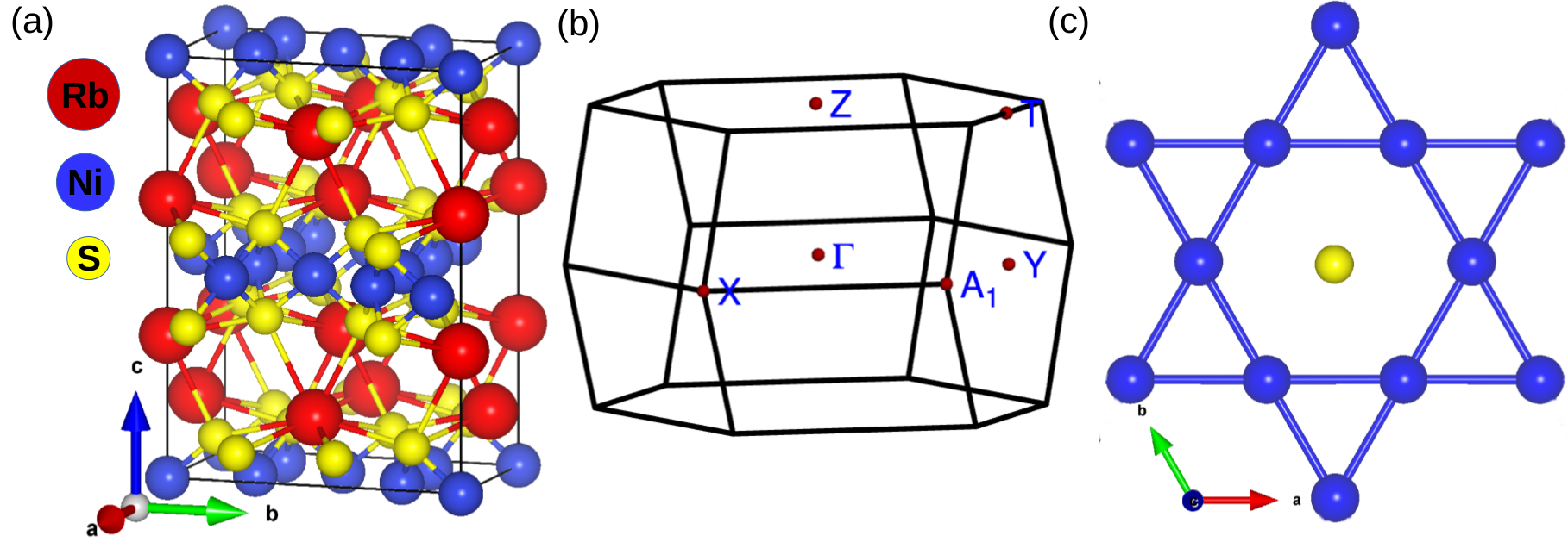
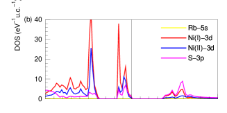
Rb2Ni3S4 crystallizes in an orthorhombic crystal structure with space group Fmmm (no. 69) and belongs to the point group D2h. The experimental lattice parameters used in this study are = 5.862 Å, = 9.937 Å and = 13.758 Å [1]. The crystal system consists of four in-equivalent atoms labeled as Rb, Ni(I), Ni(II), and S, respectively. In Rb2Ni3S4, Rb1+ ions are surrounded by eight equivalent S2- ions in an 8-coordinate geometry. The Rb–S bond distances exhibit a range from 3.38 Å to 3.45 Å. All Ni2+ ions are coordinated by four equivalent S2- ions, adopting a square co-planar arrangement [see Fig. 1(a)]. At the first and second Ni2+ site, the Ni–S bond length measured are 2.22 Å. Furthermore, Rb2Ni3S4 exhibits symmorphic crystal symmetry, and due to the presence of a center of inversion, they are considered centrosymmetric crystal. Table 1 presents the fully relaxed atomic coordinates for Rb2Ni3S4.
In order to investigate the electronic and optical characteristics of selected compound, we employed the DFT approach using the full potential local orbital (FPLO) code [18], version 18.00. The standard generalized gradient approximation (GGA) with the Perdew, Burke, and Ernzerhof (PBE-96) [19] parameterization was taken into the exchange and correlation energy. Both, scalar-relativistic (without spin-orbit coupling) and full-relativistic (with spin-orbit coupling) modes were considered for the self-consistent calculations. However, since the inclusion of spin-orbit coupling did not significantly impact the electronic properties, we focus our discussion only on the outcomes from the scalar-relativistic calculations. For the optical property calculations, we used the FOPTICS module of the FPLO. In the electronic structure calculations, a k-mesh subdivision of was used to cover the full Brillouin zone. As for the optical property calculations, a finer k-mesh subdivision of was employed. To ensure the accuracy of the energy, the convergence criteria for self-consistency as set to 10-8 Hartree. During the structural optimization, a force convergence of 10-3 eV/Å was applied.
| Atom | Point location | x | y | z |
|---|---|---|---|---|
| Rb | 8i | 0 | 0 | 0.3425 |
| Ni(I) | 8e | -1/4 | -1/4 | 0 |
| Ni(II) | 4a | 0 | 0 | 0 |
| S | 16m | 0 | 0.1677 | 0.1061 |
3 Results and discussion
3.1 Electronic properties
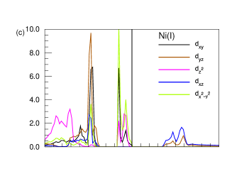
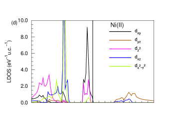
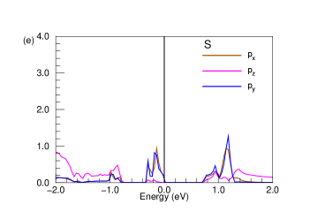
To understand the electronic properties, we performed the density of states (DOS) and band structure calculation. Based on the total and partial DOS analysis, as shown in Fig. 2, it is evident that 3d orbital of Ni and 3p orbital of S atoms contribute significantly to the DOS, while Rb has minor contributions (see Fig. 2(b)). This difference is due to the presence of only one electron in the outermost 5s orbital of Rb atom. To enhance clarity, we display the local DOS projections individually, focusing on Ni(I)-3d as depicted in Figure 2(c), and of Ni(II)-3d as shown in Figure 2(d). The analysis of the local DOS (LDOS) projection (see Fig. 2(c-e)) reveals that the insulating behavior originates from the splitting of energy bands due to the crystal field effect. It is well-established that each nickel (Ni) ion is surrounded by four S ions, forming a tetrahedral square planar coordination arrangement (see Fig. 1(a)). In this scenario, the S2- ions act as strong ligand for the central Ni2+ metal, which leads to crystal field splitting. Consequently, specific d-orbitals (, , ), known as the t2g state, possess higher energy levels compared to and orbitals, referred to as the eg state. Furthermore, below the E, a pronounced hybridization occurs between the S-3px and S-3py orbitals with the Ni-3, , and orbitals in the energy range spanning from 0 to -0.035 eV. Conversely, above E, S-3px and S-3py orbitals exhibit significant hybridization with the Ni-3 and Ni-3 orbitals within the energy range from 0.7 to 1.2 eV (see Fig. 2(c-e)).
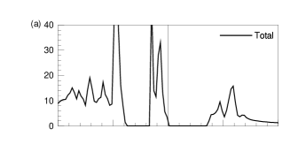
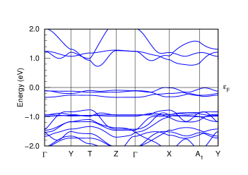
Additionally, the kagome lattice of Ni2+ leads to the formation of flat bands below E, which is mainly contributed by 3dxy orbital of Ni atom. Theoretical studies have suggested that such flat band systems in a kagome lattice can give rise to various exotic many-body phenomena [20, 16, 21, 22, 23]. Based on the analysis of the electronic band structure, Rb2Ni3S4 exhibit semiconducting behavior with an energy band gap of 0.67 eV. These findings are consistent with the previously reported DFT value of 0.66 eV [24] and the experimental value of 0.8 eV deduced from a transport study [16]. The nature of the band gap is indirect. This is attributed to the occurrence of the VBM at the high symmetry point X and the CBM at the T-Z line in the momentum space (see Fig. 3).
3.2 Optical properties
The linear response of the system to electromagnetic radiation, which is associated to the interaction of photons with electrons, can be defined using the complex dielectric function, .
| (3.1) |
where, and are the real and imaginary part of the dielectric function, respectively [25, 26].
In accordance with the selection criteria, the momentum matrix elements between the occupied and unoccupied state are used to calculate the imaginary component of the dielectric function, which is given by the following equation [27, 28],
| (3.2) |
where p is the momentum operator. The Fermi distribution function is indicated by f(kg), and Ekg is the eigenvalue associated with eigenfunction . The real part is given by Kramers-Kronig relationship [29],
| (3.3) |
The optical conductivity and electron loss function is given by following the equation,
| (3.4) |
| (3.5) |
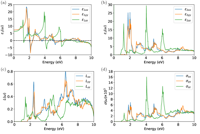
As already observed from electronic structure calculations, Rb2Ni3S4 exhibits a semiconducting nature with a band gap of 0.67 eV. Thus when exposed to incident photons, transitions can be possible at arbitrarily high photon energy. In such transitions, photons excite electrons from occupied states in the valence band region to unoccupied states in the conduction band region known as interband transition [30]. To understand these phenomena, to study the underlying optical properties, we consider the polarization components along the x, y, and z directions due to an orthorhombic crystal structure. To understand the electronic polarizability of the material under an applied electric field, we analyze the real part of the dielectric function [31], as depicted in Fig. 4(a). along x, y and z direction denoted by , , and , respectively. The real part of the dielectric function at zero frequency, (which is connected to the material’s band gap is known as static dielectric constants (0)) are found to be 7.5 along both the x and y directions, while it is 6.2 along the z direction. Correspondingly, the refractive index was determined using the established Penn Relation n(0) = [32] gives the static refractive index as 2.74 along x and y direction while 2.49 along z direction. The obtained value shows that the material has optical anisotropy. In the energy range 0 to 1.3 eV for the x, y direction, and 0 to 1 eV for the z direction, we observe a gradual increase in , which indicates that the material interaction effectively with photons. Notably, at 1.63 eV, 1.60 eV, and 1.16 eV for , , and , respectively, sharp peaks are observed. These peaks correspond to the inter-band transition, indicating the photon-induced electron transitions from occupied valence bands to the unoccupied conduction bands. This means that the material can absorb light particularly well at that specific energy. Within the photon energy range exceeding 1.16 eV, the real part of the dielectric function exhibits a remarkable characteristic: it adopts a negative value. This phenomenon is indicative of incident light being reflected by the medium. Consequently, the material demonstrates metallic attributes in this specific energy range [33, 34]. Furthermore, we also observe sharp peaks at approximately 2.01 eV, 1.96 eV, and 3.93 eV for x, y and z direction, respectively. , the imaginary part of the dielectric function, reveals details about optical absorption in crystal. The absorption begins at 0.84 eV for the imaginary part of the dielectric function, which act as the threshold energy associated with the occurrence of an optical band gap (see Fig. 4(b)). Beyond the threshold point, curve increases rapidly. Notably, sharp peaks are seen along the x, y, and z directions, respectively, at 2.02 eV, 1.97 eV, and 1.22 eV. These absorption peaks may clearly be associated with transitions from the Ni(3d) valence band to the S(3p) conduction band based on the predicted PDOS (see Fig. 2(b)). Additionally, within the energy range of 2.83 eV to 6.05 eV, various significant peaks are observed. These peaks correspond to inter-band transitions from the valence band to the conduction band [35, 36]. However, beyond the energy of 6.05 eV, the peaks begin to diminish, eventually disappearing at higher energy ranges. Another important optical property calculated in this work is the electron energy loss function L(). Fig 4(c) shows the variation of L() with photon energy. The L() provides the information about the energy loss of a fast-moving electron traversing in the material, and is reciprocal of the imaginary part of the complex dielectric function [37, 38]. The visible area of the loss spectrum exhibits a slight energy loss, which rises as photon energy increases. The identified peaks in the L() spectra provide information about the material’s plasma frequency. The nature of the material, i.e., whether it exhibits metallic properties or dielectric behavior, is known to be described by the plasma frequency. It is well known that materials exhibit metallic [ 0] behavior below the plasma resonance frequency and dielectric [ 0] behavior above this frequency [34, 39, 40, 41]. The maximal peaks for Lxx, Lyy, and Lzz are clearly visible in the energy loss spectra at approximately 6.44 eV, 6.41 eV, and 4.91 eV, respectively. The resonant energy loss is seen at 6.44 eV along x direction with a maximum value of 0.8. After these peaks, the spectrum starts to decline. In Fig. 4(d), show the optical conductivity which depend on photon energy. This indicating that the Rb2Ni3S4 exhibits optical activity in the range from 1.25 eV to 8.60 eV. The edge starts 0.84 eV, which corresponds to the calculated optical band gap of the material, and numerous peaks are observed in the spectrum. Maximum optical conductivity, , and was found to be 6.5103 Ohm-1cm-1, 16103 Ohm-1cm-1 and 5.9103 Ohm-1cm-1, respectively at photon energy of 2.02 eV to 4.05 eV. These findings are consistent with the imaginary part of the dielectric function, results obtained in Fig. 4(b).
4 Conclusions
We have investigated the electronic structure and optical properties of Rb2Ni3S4 by means of density functional theory approach. The studied material is found to be nonmagnetic semiconductor with an indirect band gap of 0.67 eV. The Ni atoms form a kagome lattice in a two-dimensional plane resulting in a flat band located below the Fermi energy. From the optical properties calculations, the dielectric function including its real and imaginary parts, the loss function, and the optical conductivity has been obtained. We found that the material is optically active in the visible and lower ultraviolet region. We predicti that Rb2Ni3S4 could be a promising candidate for optoelectronic device fabrication.
Acknowledgments
M.P.G. was supported by a grant from UNESCO-TWAS and the Swedish International Development Cooperation Agency (SIDA). The views expressed herein do not necessarily represent those of UNESCO-TWAS, SIDA or its Board of Governors. M.P.G. acknowledges IFW-Dresden for providing the large-scale compute nodes to Tribhuvan University for scientific computations. G.B.A. thanks Nepal Academy of Science and Technology (NAST) for the PhD fellowship. The author thanks Manuel Richter, IFW-Dresden for careful reading of the manuscripts and suggestions. M.P.G. and G.B.A. thanks Ulrike Nitzsche for the technical assistance.
References
- [1] Bronger W, Rennau R and Schmitz D 1991 Z. fur Anorg. Allg. Chem. 597 27–32
- [2] Kang M, Ye L, Fang S, You J S, Levitan A, Han M, Facio J I, Jozwiak C, Bostwick A, Rotenberg E et al. 2020 Nat. Mater. 19 163–169
- [3] Chen D, Le C, Fu C, Lin H, Schnelle W, Sun Y and Felser C 2021 Phys. Rev. B 103 144410
- [4] Liu E, Sun Y, Kumar N, Muechler L, Sun A, Jiao L, Yang S Y, Liu D, Liang A, Xu Q et al. 2018 Nat. Phys. 14 1125–1131
- [5] Ghimire M P, Facio J I, You J S, Ye L, Checkelsky J G, Fang S, Kaxiras E, Richter M and Van Den Brink J 2019 Phys. Rev. Res. 1 032044
- [6] Yang H, Sun Y, Zhang Y, Shi W J, Parkin S S and Yan B 2017 New J. Phys. 19 015008
- [7] Kübler J and Felser C 2018 Europhys. Lett. 120 47002
- [8] Liu J and Balents L 2017 Phys. Rev. Lett. 119 087202
- [9] Ren Z, Li H, Sharma S, Bhattarai D, Zhao H, Rachmilowitz B, Bahrami F, Tafti F, Fang S, Ghimire M P et al. 2022 npj Quantum Mater. 7 109
- [10] Naher M, Ali M A, Hossain M, Uddin M and Naqib S 2023 arXiv preprint arXiv:2304.07669
- [11] Li Q, Wu Y, Fan X, Zhang Y J, Zhu X, Zhu Z, Li Y and Wen H H 2022 Phys. Rev. B 106 214501
- [12] Elder S H, Jobic S, Brec R, Gelabert M and DiSalvo F J 1996 J. Alloys Compd. 235 135–142
- [13] Acharya G B, Belbase B P and Ghimire M P 2023 Electronic Structure URL :DOI 10.1088/2516-1075/ad0951
- [14] Bronger W, Eyck J, Rüdorff W and Stöussel A 1970 Z. fur Anorg. Allg. Chem. 375 1–7
- [15] Fukamachi T, Kobayashi Y, Nakamura A, Harashina H and Sato M 1999 J. Phys. Soc. Japan 68 3668–3672
- [16] Hondou K, Fujiwara Y, Kato T, Iio K, Saiki A, Usuda M and Hamada N 2002 J. Alloys Compd. 333 274–281
- [17] Nawai S, Okazaki K, Mizokawa T, Fujimori A, Hondou K, Fujiwara Y, Iio K, Usuda M and Hamada N 2004 Phys. Rev. B 69 045103
- [18] Koepernik K and Eschrig H 1999 Phys. Rev. B 59 1743
- [19] Perdew J P, Burke K and Ernzerhof M 1996 Phys. Rev. Lett. 77 3865
- [20] Hondou K and Chikazawa S 2007 J. Magn. Magn. Mater. 310 1815–1817
- [21] Kang M, Fang S, Ye L, Po H C, Denlinger J, Jozwiak C, Bostwick A, Rotenberg E, Kaxiras E, Checkelsky J G et al. 2020 Nat. Commun. 11 1–9
- [22] Wang W S, Li Z Z, Xiang Y Y and Wang Q H 2013 Phys. Rev. B 87 115135
- [23] Yu S L and Li J X 2012 Phys. Rev. B 85 144402
- [24] Nawai S, Okazaki K, Mizokawa T, Fujimori A, Hondou K, Fujiwara Y, Iio K, Usuda M and Hamada N 2004 Phys. Rev. B 69(4) 045103
- [25] He H, Orlando R, Blanco M A, Pandey R, Amzallag E, Baraille I and Rérat M 2006 Phys. Rev. B 74 195123
- [26] Ghosh A and Thangavel R 2017 Ind. J. Phys. 91 1339–1344
- [27] Ambrosch-Draxl C and Sofo J O 2006 Comput. Phys. Commun. 175 1–14
- [28] Hoat D 2019 J. Mol. Graph. 90 153–160
- [29] Toll J S 1956 Phys. Rev. 104 1760
- [30] Stepanjuga A, Ray R, Richter M, Carrocci S, Hampel S, Galle L, Grafe H J and Valldor M 2022 New J. Chem. 46 4900–4910
- [31] Hoat D, Silva J R and Blas A M 2019 J. Solid State Chem. 270 85–91
- [32] Penn D R 1962 Phys. Rev. 128 2093
- [33] Shore A 2019 RSC Adv. 9 12813–12813
- [34] Kumar M, Raj A, Kumar A, Sharma S, Bherwani H, Gupta A and Anshul A 2021 Optik 242 166764
- [35] Kumar A and Ahluwalia P 2012 Mater. Chem. Phys. 135 755–761
- [36] Belbase B P, Jaishi D R, Adhikari R P and Ghimire M P 2023 Solid State Commun. 361 115085
- [37] Wang C and Klein B 1981 Phys. Rev. B 24 3417
- [38] Zhang X, Chen Z, Zhang S, Liu R, Zong H, Jing Q, Li G, Ma M and Wang W 2007 J. Condens. Matter Phys. 19 425231
- [39] Hu J M, Huang S P, Xie Z, Hu H and Cheng W D 2007 J. Condens. Matter Phys. 19 496215
- [40] Kumar P, Soni A, Bhamu K and Sahariya J 2017 Mater. Res. Bull. 86 131–138
- [41] Sun J, Zhou X F, Fan Y X, Chen J, Wang H T, Guo X, He J and Tian Y 2006 Phys. Rev. B 73 045108