Cryogenic hybrid magnonic circuits based on spalled YIG thin films
Abstract
Yttrium iron garnet (YIG) magnonics has sparked extensive research interests toward harnessing magnons (quasiparticles of collective spin excitation) for signal processing. In particular, YIG magnonics-based hybrid systems exhibit great potentials for quantum information science because of their wide frequency tunability and excellent compatibility with other platforms. However, the broad application and scalability of thin-film YIG devices in the quantum regime has been severely limited due to the substantial microwave loss in the host substrate for YIG, gadolinium gallium garnet (GGG), at cryogenic temperatures. In this study, we demonstrate that substrate-free YIG thin films can be obtained by introducing the controlled spalling and layer transfer technology to YIG/GGG samples. Our approach is validated by measuring a hybrid device consisting of a superconducting resonator and a spalled YIG film, which gives a strong coupling feature indicating the good coherence of our system. This advancement paves the way for enhanced on-chip integration and the scalability of YIG-based quantum devices.
The field of YIG magnonics [1] is a rapidly evolving research area dedicated to studying the collective spin excitations (magnons) in YIG (yttrium iron garnet) crystals. In recent years, it has shown extensive potential in hybrid information systems [2, 3, 4, 5]. Thanks to its low magnetic damping, high spin density, and excellent compatibility with various physical platforms, YIG has been considered as an ideal magnonic platform for hybrid quantum information processing. Researchers are actively exploring various YIG-based hybrid systems such as electromagnonics [6, 7, 8, 9, 10, 11, 12, 13], optomagnonics [14, 15, 16], and magnomechanics [17, 18, 19, 20] for different applications. As demand grows for scalable quantum systems, thin-film YIG devices are highly desired for on-chip integration over bulk YIG spheres used in earlier research.
However, the development of thin film YIG devices at cryogenic temperature regimes has been severely limited. One major obstacle is the undesirable properties of the substrate used for the growth of YIG thin film. The best growth method for high quality single crystalline YIG films is epitaxial growth on gadolinium gallium garnet (GGG) substrates which has a matched lattice constant with YIG, yielding a room-temperature magnon linewidth close to that of single-crystal YIG spheres. However, at cryogenic temperatures such YIG films exhibit very high microwave losses because the host substrate GGG undergoes a phase transition into a geometrically frustrating spin-liquid state below 5 Kelvin [21]. In this state, the short-range ordered spins in the GGG substrate shows strong absorption to external energy, a property that has found application in commercial adiabatic demagnetization cooling [22, 23]. The presence of this spin-liquid state in GGG degrades the lifetime of spin excitations in the YIG layer, as indicated by the larger FMR linewidth [24, 25, 26] compared with spheres made of pure YIG, posing a significant impediment to its integration in cryogenic quantum systems. For instance, electromagnonic systems involving strongly coupled microwave photons and magnons have been extensively studied in the past few years [6, 7, 8, 9, 10, 11, 12, 13, 27, 28, 29], which have enabled advanced functionalities such as entanglement with superconducting qubits [30, 31, 32], but most of previous demonstrations are based on YIG spheres while YIG thin films have been rarely used.
One promising solution to this grand challenge is using YIG thin films without the GGG substrate, which includes two technical approaches. The first approach is to grow YIG thin films on substrates other than GGG such as silicon [33, 34, 25, 35]. This approach is straightforward and more favorable from the aspect of device integration; however, the quality of YIG thin films are usually low because of the lattice mismatch between YIG and the new substrate. The second approach involves growth of YIG on GGG substrates with post-processing to detach YIG from the GGG substrate [36, 37, 38, 39]. This method produces high quality YIG but the separation processes for YIG are usually challenging due to the similar physical and chemical properties of YIG and GGG, hindering wide application of such technologies. In this work, we show our investigation on a new method that can simplify the YIG detaching process, providing a new direction for the development of YIG thin film devices.
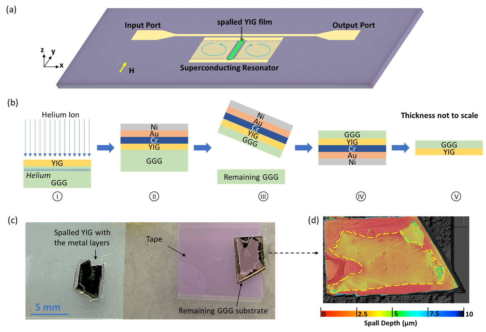
The approach we used for detaching YIG from GGG is based on controlled mechanical spalling [40], as shown by the procedures in 1(b). The substrate we used is a commercially available single-crystal YIG film [200 nm thick, (111)-oriented] grown on a 500 m-thick GGG substrate by liquid phase epitaxy (LPE). After cleaning the sample, a layer of 10-nm-thick chromium followed by 70-nm-thick gold are deposited on the YIG surface through magnetron sputtering. Using the gold layer as a seed layer, a thick layer of Ni is electroplated with a final thickness of 7 m using the electroplating conditions in reference [41], which yields an intrinsic tensile stress of 700 MPa. The tensile stress and thickness of the Ni defines an equilibrium depth within the YIG/GGG substrate at which steady state crack propagation can take place [42]. Using a thermal release tape, the top layer stack (Ni/Au/Cr/YIG/GGG) is carefully spalled, resulting in a continuous substrate-free film, as shown in Figure 1(c). Considering that this depth is larger than the thickness of the YIG layer, the spalled YIG is still attached to a thin layer of GGG. However, by choosing YIG wafers with larger YIG thickness (e.g., 10 ) and optimizing the thickness and tensile stress of the YIG layers, it is possible to obtain a spalled layer of pure YIG without any residual GGG. The final substrate-free device is obtained by removing the nickel, gold, and chromium layers with appropriate wet chemical etchants.
We noticed that with our current conditions, the spalling process is also largely affected by ion implantation in the substrate. When the substrate is intrinsic YIG/GGG sample, the resulting spalling depth is typically 5-10 um, whereas if the YIG/GGG sample is treated with helium ion implantation (following the conditions from Refs. [36, 43]), thinner spalling depths are obtained with smoother surfaces, as shown by height scan of the remaining GGG substrate using a 3D laser scanning confocal microscope [1(d)] which reveals a spalling depth of around 2-3 m. This may be attributed to the fact that the GGG layer above the ion implantation depth (7 m) is damaged by the high-energy helium ions during the implanting process and becomes easier to break under the elastic stress from the Ni layer, resulting in a shallower spalling depth.
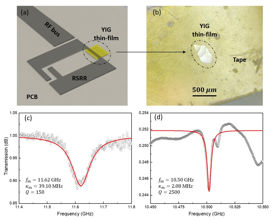
To characterize the microwave performance of the spalled YIG thin film at room temperature, it is flip-bonded to a rectangle split ring resonator (RSRR) made of copper [13] to test the ferromagnetic resonance (FMR) response, as schematically illustrated by Fig. 2(a). The reflection spectrum of the RSRR is obtained using a vector network analyzer. When an out-of-plane bias magnetic field is tuned to sweep the FMR frequency, it is expected that the magnon mode becomes visible in the spectrum when it is tuned very close to the microwave resonator frequency. However, when a flake from the spalled YIG film (which has been treated with helium ion implantation) is bonded on the RSRR, no magnon modes can be observed from the RSRR reflection spectra. This is speculated as the result of the large magnon linewidth in the YIG flake and the small volume of the YIG flake (accordingly small coupling with the RSRR resonator). To verify this speculation, we tested a larger piece (roughly 5mm lateral size) of unspalled YIG that was treated through the same ion implantation process, using the same RSRR reflection measurement. With the increased YIG volume, the magnon mode is successfully observed, but the measured data [Fig. 2(c)] shows a notably high dissipation rate MHz at 11.6 GHz, which is one order of magnitude higher than previously reported values on single-crystal YIG thin films [13]. Such elevated disspation rates can be attributed to two possible sources of dissipation: (1) The damage to the crystalline structure caused by the high-energy ions penetrating the YIG layer, and (2) The accumulated helium ions in the YIG layer. Both effects can be mitigated using an annealing process, which will restore the damaged lattice structure and repel the accumulated helium ions from YIG. We carried out an annealing process for multiple flakes of the substrate-free YIG film in ambient air, reaching a maximum temperature of 850 ∘C. The samples is gradually heated from room temperature to 850 ∘C over a period of 6 hours, followed by a 3-hour hold at the maximum temperature, and then a slow cooling process over a span of 14 hours to room temperature, providing ample time for the repair of the YIG crystalline lattice. After the annealing process, the magnon mode shows up on a device with a small YIG flake (around ), as shown in Fig. 2(d). Numerical fitting shows a dissipation rage of MHz at 10.5 GHz, which is comparable with those of high-quality LPE YIG thin films reported in previous articles [24, 44, 13].
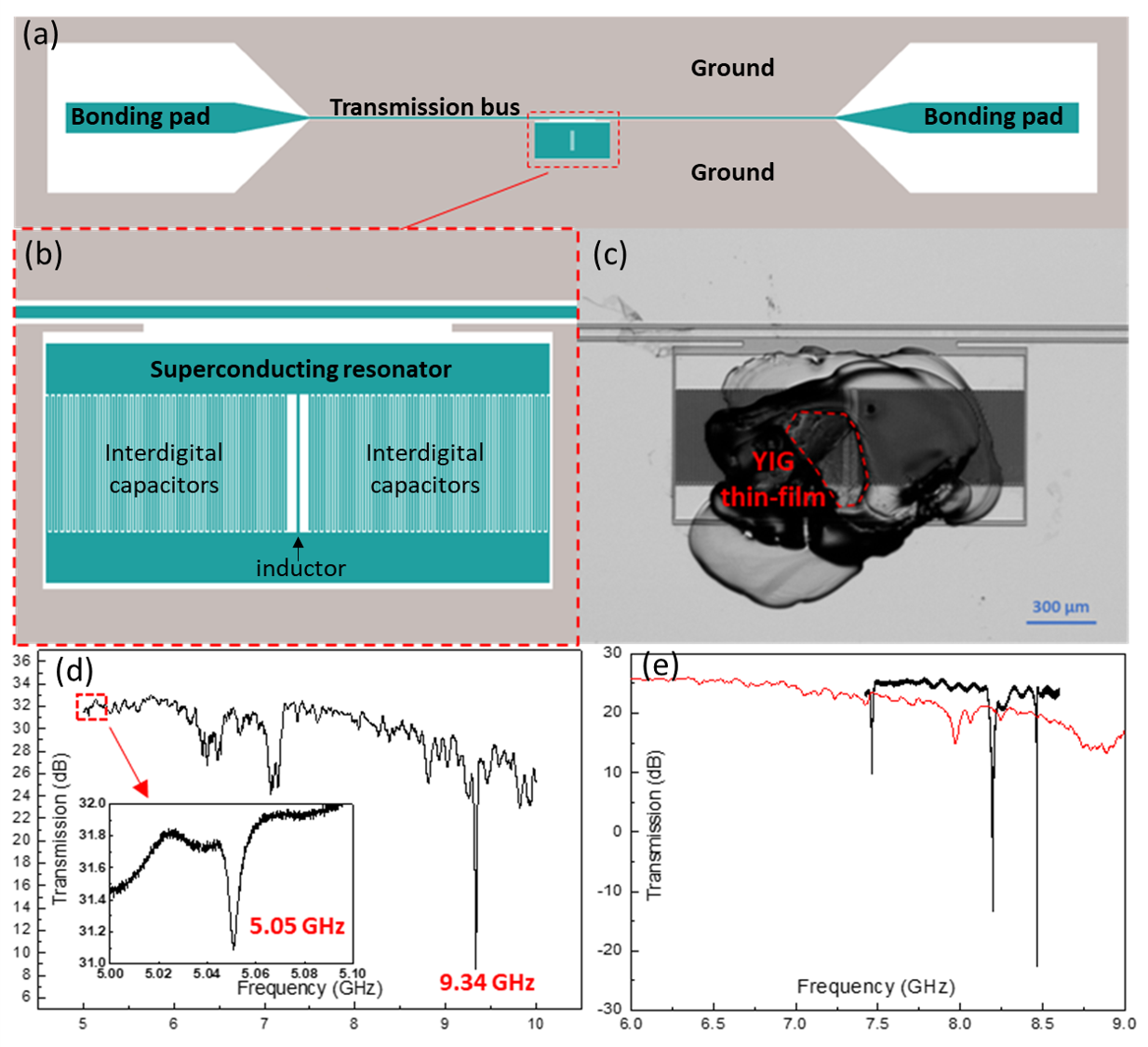
To further demonstrate its potential for cryogenic quantum operations, the spalled YIG thin films are further characterized at millikelvin (mk) temperature. A superconducting resonator is used to couple with the YIG flake, which is fabricated using 100-nm-thik niobium through photolithography and dry etching. To enhance the magnon-photon coupling, a lumped-element resonator with interdigital capacitors is used, which is inductively couples to a bus transmission line, as shown by the layout plot in Figs. 3(a) and (b). The YIG flake is flip-bonded using GE varnish to cover the center inductor line where the microwave magnetic field is the strongest, which further enhances the coupling strength between the magnon and photon modes. An optical image of the assembled device is shown in Fig. 3(c)], where the position of the spalled YIG flake is outlined by the red dashed curve.
Figure 3(d) depicts the measured microwave transmission of our device at a temperature of 200 millikelvin performed within an adiabatic demagnetization refrigerator (ADR). Two resonance modes can be observed as the two sharp dips in the transmission spectrum, similar to what is observed in Ref.[28]. The inset highlights the fundamental mode at 5.05 GHz which has a lower damping rate and smaller extinction ratio. The higher-order mode at 9.34 GHz has a larger extinction ratio and larger dissipation rate but it couples weakly with the YIG magnon mode and thus will not be discussed further. Importantly, the clear observation of two high-quality resonances on the YIG-loaded superconducting resonator indicates that the effect of the GGG substrate has been significantly suppressed. As a comparison, we measured another superconducting resonator device at the same temperature (200 mK), which is loaded with a regular YIG thin film with the m-thick GGG substrate still attached. From the measurement results in Fig. 3(e) (red curve), no clear microwave resonances can be observed, indicating the significantly increased loss on the superconducting resonator, while prior to the YIG/GGG bonding two resonances (at 7.4 GHz and 8.5 GHz) are clearly visible [black curve in Fig. 3(e)].
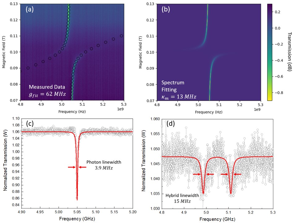
To further investigate the performance of the device shown in Fig. 3(c), a series of transmission spectra are collected while a magnetic field is swept to tune the magnon frequency. The magnetic field is applied parallel to the surface of the superconducting resonator chip, aligning with the direction of the inductor wire. A clear avoid-crossing feature is observed in the measured spectra, as shown in Fig. 4(a), indicating that our device has entered the strong coupling regime, where the magnon-photon coupling strength exceeds the dissipation rate of each individual mode.
Using numerical fitting based on rotating-wave approximation (RWA) [45], the magnon-photon coupling strength is extracted as 62 MHz, with detailed procedures described in Section II of the supplemental material [46]. The two branches of the calculated magnon-photon mode frequencies, represented by the red dots in Fig. 4(a), match well with the measured spectrum. At a magnetic field of 1300 G where the magnon mode is large detuned from the microwave resonance, the dissipation rate of the microwave modeis extracted as MHz, which leads to a quality factor . Considering that the YIG flake is positions sufficiently far from the bus transmission line, its direct coupling with the bus waveguide is negligible. Therefore, the magnon mode is observed only when its frequency is close to or on-resonance with the microwave resonance. We can estimate the magnon dissipation rate using the relation when the two modes are maximally hybridized (when magnon and photon modes are on resonance). Here is the on-resonance linewidth of the hybrid mode, which is fitted to be 15 MHz as presented in Fig. 4(d). Accordingly, the dissipation rate of the magnon mode is determinate to be MHz. Compared with previous devices which have YIG on the 500-m-thick GGG, the linewidth of the magnon has been significantly reduced. Although it is still higher than the linewidths measured on bulk YIG samples, it may be attributed to residual GGG layer attached to the YIG thin film which can be removed through futher optimization. Such calculation result is consistent with our fitting results based on the input-output theory [47, 48, 49], as described by equation
| (1) |
where represent the magnon-photon coupling strength, represents the external coupling rate between the microwave resonator and the bus feeding line, () represents the total dissipation rate of the resonator (magnon) mode, and represent the detuning of the driving frequency from the microwave resonance and magnon frequency, respectively. The calculated spectra using Eq. 1 are plotted in Fig. 4(b), which match well with the measured result in Fig. 4(a). For a comprehensive exploration of the fitting procedures and detailed results, we direct readers to the Supplemental Material [46].
In conclusion, we have demonstrated a new approach for developing substrate-free YIG thin films, and validated the our method by measuring the strong magnon-photon coupling on a hybrid device. The direct comparison with conventional YIG/GGG devices confirmed the effectiveness of our approach. Our discovery represents the first application of the spalling technology on magnetic garnets, which have been known as very strong and hard to process. Compared with other approaches, our spalling-based method offers distinct advantages including reduced material contamination and flexible thickness control. Although the linewidth of our measured device at cryogenic temperatures is still higher compared with bulk YIG, it can be further improved by completely removing the GGG substrate. Upon further optimization, including the thickness of the original YIG film as well as the stress and thickness of the Ni layer, our approach is promising for wafer-scale production of magnonic devices for quantum applications and beyond. In particular, when combined with recent experimental techniques [16, 50, 13] for YIG magnonic devices, our substrate-free YIG thin films may offer unique properties for magnons to couple with a broad range of degrees of freedom, including optics, mechanics, and magnetics.
Acknowledgements.
The authors thank R. Divan, L. Stan, C. Miller, and D. Czaplewski for support in the device fabrication. X.Z. acknowledges support from ONR YIP (N00014-23-1-2144). Contributions by C.H. and S.G. were supported by the Vannevar Bush Fellowship received by S.G. under the program sponsored by the Office of the Undersecretary of Defense for Research and Engineering and in part by the Office of Naval Research as the Executive Manager for the grant. Work performed at the Center for Nanoscale Materials, a U.S. Department of Energy Office of Science User Facility, was supported by the U.S. DOE Office of Basic Energy Sciences, under Contract No. DE-AC02-06CH11357.† guha@uchicago.edu
‡ xu.zhang@northeastern.edu
∗ J. Xu and C. Horn contributed equally to this work.
References
- Serga et al. [2010] A. A. Serga, A. V. Chumak, and B. Hillebrands, YIG magnonics, J. Phys. D: Appl. Phys. 43, 264002 (2010).
- Awschalom et al. [2021] D. D. Awschalom, C. R. Du, R. He, F. J. Heremans, A. Hoffmann, J. Hou, H. Kurebayashi, Y. Li, L. Liu, V. Novosad, et al., Quantum engineering with hybrid magnonic systems and materials, IEEE Transactions on Quantum Engineering 2, 1 (2021).
- Li et al. [2020] Y. Li, W. Zhang, V. Tyberkevych, W.-K. Kwok, A. Hoffmann, and V. Novosad, Hybrid magnonics: Physics, circuits, and applications for coherent information processing, Journal of Applied Physics 128, 130902 (2020).
- Zhang [2023] X. Zhang, A review of common materials for hybrid quantum magnonics, Materials Today Electronics 5, 100044 (2023).
- Lachance-Quirion et al. [2019] D. Lachance-Quirion, Y. Tabuchi, A. Gloppe, K. Usami, and Y. Nakamura, Hybrid quantum systems based on magnonics, Applied Physics Express 12, 070101 (2019).
- Zhang et al. [2014] X. Zhang, C.-L. Zou, L. Jiang, and H. X. Tang, Strongly coupled magnons and cavity microwave photons, Phys. Rev. Lett. 113, 156401 (2014).
- Bai et al. [2015] L. Bai, M. Harder, Y. P. Chen, X. Fan, J. Q. Xiao, and C.-M. Hu, Spin pumping in electrodynamically coupled magnon-photon systems, Phys. Rev. Lett. 114, 227201 (2015).
- Harder and Hu [2018] M. Harder and C.-M. Hu, Cavity spintronics: an early review of recent progress in the study of magnon–photon level repulsion, Solid State Physics 69, 47 (2018).
- Bhoi and Kim [2020] B. Bhoi and S.-K. Kim, Roadmap for photon-magnon coupling and its applications, in Solid State Physics, Vol. 71 (Elsevier, 2020) pp. 39–71.
- Hu [2020] C.-M. Hu, The 2020 roadmap for spin cavitronics, in Solid State Physics, Vol. 71 (Academic Press, Cambridge, MA, USA, 2020) pp. 117–121.
- Rameshti et al. [2022] B. Z. Rameshti, S. V. Kusminskiy, J. A. Haigh, K. Usami, D. Lachance-Quirion, Y. Nakamura, C.-M. Hu, H. X. Tang, G. E. Bauer, and Y. M. Blanter, Cavity magnonics, Physics Reports 979, 1 (2022).
- Rao et al. [2019] J. W. Rao, S. Kaur, B. M. Yao, E. R. J. Edwards, Y. T. Zhao, X. Fan, D. Xue, T. J. Silva, Y. S. Gui, and C.-M. Hu, Analogue of dynamic Hall effect in cavity magnon polariton system and coherently controlled logic device, Nat. Commun. 10, 1 (2019).
- Xu et al. [2021a] J. Xu, C. Zhong, X. Han, D. Jin, L. Jiang, and X. Zhang, Coherent Gate Operations in Hybrid Magnonics, Phys. Rev. Lett. 126, 207202 (2021a).
- Zhang et al. [2016a] X. Zhang, N. Zhu, C.-L. Zou, and H. X. Tang, Optomagnonic Whispering Gallery Microresonators, Phys. Rev. Lett. 117, 123605 (2016a).
- Bi et al. [2011] L. Bi, J. Hu, P. Jiang, D. H. Kim, G. F. Dionne, L. C. Kimerling, and C. A. Ross, On-chip optical isolation in monolithically integrated non-reciprocal optical resonators, Nat. Photonics 5, 758 (2011).
- Zhu et al. [2020] N. Zhu, X. Zhang, X. Zhang, X. Han, X. Han, C.-L. Zou, C.-L. Zou, C. Zhong, C. Zhong, C.-H. Wang, C.-H. Wang, L. Jiang, L. Jiang, and H. X. Tang, Waveguide cavity optomagnonics for microwave-to-optics conversion, Optica 7, 1291 (2020).
- Seo et al. [2017] Y.-J. Seo, K. Harii, R. Takahashi, H. Chudo, K. Oyanagi, Z. Qiu, T. Ono, Y. Shiomi, and E. Saitoh, Fabrication and magnetic control of Y3Fe5O12 cantilevers, Appl. Phys. Lett. 110, 10.1063/1.4979553 (2017).
- An et al. [2020] K. An, A. N. Litvinenko, R. Kohno, A. A. Fuad, V. V. Naletov, L. Vila, U. Ebels, G. de Loubens, H. Hurdequint, N. Beaulieu, J. Ben Youssef, N. Vukadinovic, G. E. W. Bauer, A. N. Slavin, V. S. Tiberkevich, and O. Klein, Coherent long-range transfer of angular momentum between magnon Kittel modes by phonons, Phys. Rev. B 101, 060407 (2020).
- Zhang et al. [2016b] X. Zhang, C.-L. Zou, L. Jiang, and H. X. Tang, Cavity magnomechanics, Sci. Adv. 2, 10.1126/sciadv.1501286 (2016b).
- Xu et al. [2021b] J. Xu, C. Zhong, X. Zhou, X. Han, D. Jin, S. K. Gray, L. Jiang, and X. Zhang, Coherent Pulse Echo in Hybrid Magnonics with Multimode Phonons, Phys. Rev. Appl. 16, 024009 (2021b).
- Petrenko et al. [1997] O. A. Petrenko, C. Ritter, M. Yethiraj, and D. M. Paul, Spin-liquid behavior of the gadolinium gallium garnet, Physica B 241-243, 727 (1997).
- Hepburn et al. [1994] I. D. Hepburn, A. Smith, and I. Davenport, Adiabatic Demagnetisation Refrigerators for Space Applications on JSTOR (1994), [Online; accessed 19. Oct. 2023].
- Kwon et al. [2022] D. Kwon, J. Bae, and S. Jeong, Development of the integrated sorption cooler for an adiabatic demagnetization refrigerator (ADR), Cryogenics 122, 103421 (2022).
- Kosen et al. [2019] S. Kosen, A. F. van Loo, D. A. Bozhko, L. Mihalceanu, and A. D. Karenowska, Microwave magnon damping in YIG films at millikelvin temperatures, APL Mater. 7, 10.1063/1.5115266 (2019).
- Guo et al. [2022] S. Guo, B. McCullian, P. Chris Hammel, and F. Yang, Low damping at few-K temperatures in Y3Fe5O12 epitaxial films isolated from Gd3Ga5O12 substrate using a diamagnetic Y3Sc2.5Al2.5O12 spacer, J. Magn. Magn. Mater. 562, 169795 (2022).
- Jermain et al. [2017] C. L. Jermain, S. V. Aradhya, N. D. Reynolds, R. A. Buhrman, J. T. Brangham, M. R. Page, P. C. Hammel, F. Y. Yang, and D. C. Ralph, Increased low-temperature damping in yttrium iron garnet thin films, Phys. Rev. B 95, 174411 (2017).
- Li et al. [2019] Y. Li, T. Polakovic, Y.-L. Wang, J. Xu, S. Lendinez, Z. Zhang, J. Ding, T. Khaire, H. Saglam, R. Divan, J. Pearson, W.-K. Kwok, Z. Xiao, V. Novosad, A. Hoffmann, and W. Zhang, Strong Coupling between Magnons and Microwave Photons in On-Chip Ferromagnet-Superconductor Thin-Film Devices, Phys. Rev. Lett. 123, 107701 (2019).
- Hou and Liu [2019] J. T. Hou and L. Liu, Strong Coupling between Microwave Photons and Nanomagnet Magnons, Phys. Rev. Lett. 123, 107702 (2019).
- Xu et al. [2021c] J. Xu, C. Zhong, X. Han, D. Jin, L. Jiang, and X. Zhang, Coherent Gate Operations in Hybrid Magnonics, Phys. Rev. Lett. 126, 207202 (2021c).
- Tabuchi et al. [2015] Y. Tabuchi, S. Ishino, A. Noguchi, T. Ishikawa, R. Yamazaki, K. Usami, and Y. Nakamura, Coherent coupling between a ferromagnetic magnon and a superconducting qubit, Science 349, 405 (2015).
- Lachance-Quirion et al. [2020] D. Lachance-Quirion, S. P. Wolski, Y. Tabuchi, S. Kono, K. Usami, and Y. Nakamura, Entanglement-based single-shot detection of a single magnon with a superconducting qubit, Science 367, 425 (2020).
- Xu et al. [2023] D. Xu, X.-K. Gu, H.-K. Li, Y.-C. Weng, Y.-P. Wang, J. Li, H. Wang, S.-Y. Zhu, and J. Q. You, Quantum Control of a Single Magnon in a Macroscopic Spin System, Phys. Rev. Lett. 130, 193603 (2023).
- Bi et al. [2013] L. Bi, J. Hu, P. Jiang, H. S. Kim, D. H. Kim, M. C. Onbasli, G. F. Dionne, and C. A. Ross, Magneto-Optical Thin Films for On-Chip Monolithic Integration of Non-Reciprocal Photonic Devices, Materials 6, 5094 (2013).
- Onbasli et al. [2014] M. C. Onbasli, T. Goto, X. Sun, N. Huynh, and C. A. Ross, Integration of bulk-quality thin film magneto-optical cerium-doped yttrium iron garnet on silicon nitride photonic substrates, Opt. Express 22, 25183 (2014).
- Guo et al. [2023] S. Guo, D. Russell, J. Lanier, H. Da, P. C. Hammel, and F. Yang, Strong on-Chip Microwave Photon–Magnon Coupling Using Ultralow-Damping Epitaxial Y3Fe5O12 Films at 2 K, Nano Lett. 23, 5055 (2023).
- Levy et al. [1998a] M. Levy, R. M. Osgood, A. Kumar, and H. Bakhru, Crystal ion slicing of single-crystal magnetic garnet films, J. Appl. Phys. 83, 6759 (1998a).
- Heyroth et al. [2019] F. Heyroth, C. Hauser, P. Trempler, P. Geyer, F. Syrowatka, R. Dreyer, S. G. Ebbinghaus, G. Woltersdorf, and G. Schmidt, Monocrystalline Freestanding Three-Dimensional Yttrium-Iron-Garnet Magnon Nanoresonators, Phys. Rev. Appl. 12, 054031 (2019).
- Haigh et al. [2020] J. A. Haigh, R. A. Chakalov, and A. J. Ramsay, Subpicoliter Magnetoptical Cavities, Phys. Rev. Appl. 14, 044005 (2020).
- Baity et al. [2021] P. G. Baity, D. A. Bozhko, R. Macêdo, W. Smith, R. C. Holland, S. Danilin, V. Seferai, J. Barbosa, R. R. Peroor, S. Goldman, U. Nasti, J. Paul, R. H. Hadfield, S. McVitie, and M. Weides, Strong magnon–photon coupling with chip-integrated YIG in the zero-temperature limit, Appl. Phys. Lett. 119, 10.1063/5.0054837 (2021).
- Bedell et al. [2012] S. W. Bedell, D. Shahrjerdi, B. Hekmatshoar, K. Fogel, P. A. Lauro, J. A. Ott, N. Sosa, and D. Sadana, Kerf-Less Removal of Si, Ge, and III–V Layers by Controlled Spalling to Enable Low-Cost PV Technologies, IEEE J. Photovoltaics 2, 141 (2012).
- Bedell et al. [2017] S. W. Bedell, P. Lauro, J. A. Ott, K. Fogel, and D. K. Sadana, Layer transfer of bulk gallium nitride by controlled spalling, J. Appl. Phys. 122, 10.1063/1.4986646 (2017).
- Suo and Hutchinson [1989] Z. Suo and J. W. Hutchinson, Steady-state cracking in brittle substrates beneath adherent films, Int. J. Solids Struct. 25, 1337 (1989).
- Levy et al. [1998b] M. Levy, R. M. Osgood, R. Liu, L. E. Cross, G. S. Cargill, A. Kumar, and H. Bakhru, Fabrication of single-crystal lithium niobate films by crystal ion slicing, Appl. Phys. Lett. 73, 2293 (1998b).
- Castel et al. [2016] V. Castel, A. Manchec, and J. B. Youssef, Control of Magnon-Photon Coupling Strength in a Planar Resonator/Yttrium-Iron-Garnet Thin-Film Configuration, IEEE Magn. Lett. 8, ArticleSequenceNumber:3703105 (2016).
- Boyd [2008] R. W. Boyd, Nonlinear Optics (Elsevier, Academic Press, 2008).
- [46] Supplemental material .
- Schuster et al. [2010] D. I. Schuster, A. P. Sears, E. Ginossar, L. DiCarlo, L. Frunzio, J. J. L. Morton, H. Wu, G. A. D. Briggs, B. B. Buckley, D. D. Awschalom, and R. J. Schoelkopf, High-Cooperativity Coupling of Electron-Spin Ensembles to Superconducting Cavities, Phys. Rev. Lett. 105, 140501 (2010).
- Walls and Milburn [2008] D. Walls and G. J. Milburn, Quantum Optics (Springer, Berlin, Germany, 2008).
- Chen et al. [2022] Q.-M. Chen, M. Pfeiffer, M. Partanen, F. Fesquet, K. E. Honasoge, F. Kronowetter, Y. Nojiri, M. Renger, K. G. Fedorov, A. Marx, F. Deppe, and R. Gross, Scattering coefficients of superconducting microwave resonators. I. Transfer matrix approach, Phys. Rev. B 106, 214505 (2022).
- Heinz et al. [2020] B. Heinz, T. Brächer, M. Schneider, Q. Wang, B. Lägel, A. M. Friedel, D. Breitbach, S. Steinert, T. Meyer, M. Kewenig, C. Dubs, P. Pirro, and A. V. Chumak, Propagation of Spin-Wave Packets in Individual Nanosized, Nano Lett. 20, 4220 (2020).