Also at ]State Key Laboratory of Terahertz and Millimeter Waves, City University of Hong Kong, Kowloon, Hong Kong, China.
Advancing large-scale thin-film PPLN nonlinear photonics with segmented tunable micro-heaters
Abstract
Thin-film periodically poled lithium niobate (TF-PPLN) devices have recently gained prominence for efficient wavelength conversion processes in both classical and quantum applications. However, the patterning and poling of TF-PPLN devices today are mostly performed at chip scales, presenting a significant bottleneck for future large-scale nonlinear photonic systems that require the integration of multiple nonlinear components with consistent performance and low cost. Here, we take a pivotal step towards this goal by developing a wafer-scale TF-PPLN nonlinear photonic platform, leveraging ultraviolet stepper lithography and an automated poling process. To address the inhomogeneous broadening of the quasi-phase matching (QPM) spectrum induced by film thickness variations across the wafer, we propose and demonstrate segmented thermal optic tuning modules that can precisely adjust and align the QPM peak wavelengths in each section. Using the segmented micro-heaters, we show the successful realignment of inhomogeneously broadened multi-peak QPM spectra with more than doubled peak second-harmonic generation efficiency. The advanced fabrication techniques and segmented tuning architectures presented herein pave the way for wafer-scale integration of complex functional nonlinear photonic circuits with applications in quantum information processing, precision sensing and metrology, and low-noise-figure optical signal amplification.
I INTRODUCTION
Thin-film periodically poled lithium niobate (TF-PPLN) devices, renowned for their strong optical nonlinearity and excellent light confinement, are essential nonlinear photonic building blocks for the next generation of optical communication and quantum information processing systems [1]. Due to the substantially enhanced optical intensity in tightly confined waveguides, TF-PPLN wavelength convertors exhibit more than one order of magnitude higher normalized conversion efficiencies compared to their bulk counterparts[2, 3, 4]. These highly efficient TF-PPLN waveguides have enabled many high-performance nonlinear devices, including resonator-based ultra-efficient wavelength converters [5, 6], broadband optical parametric amplifiers [7, 8] and entangled photon-pair sources [9, 10]. Moreover, TF-PPLN devices enjoy excellent compatibility with other on-chip functional photonic devices available on the thin-film lithium niobate (TFLN) platform, such as integrated EO modulators [11, 12], acousto-optic modulators [13], frequency combs [14, 15, 16], as well as heterogeneously integrated lasers [17] and photodetectors [18, 19, 20]. By now, this integration compatibility has empowered chip-scale nonlinear and quantum photonic systems with unprecedented performances, including efficient quantum squeezers [21, 22], femtosecond all-optical switches [23], octave-spanning optical parametric oscillators [24], and integrated Pockels lasers co-lasing at infrared and visible wavelengths [25]. Additionally, to facilitate the active control of quasi-phase-matching (QPM) wavelength, thermally tunable TF-PPLN waveguides with high tuning efficiencies have also been developed [26]. Despite the remarkable achievements of TF-PPLN devices, their fabrication today still relies on waveguide patterning and crystal poling processes performed on individually centimeter-sized chips based on electron-beam lithography and manual poling. In recent years, wafer-scale fabrication techniques have been developed for TFLN devices with passive or electro-optic functionalities [27]; however, these processes have not yet been extended to include nonlinear photonic devices like TF-PPLN waveguides. This limitation persists mainly due to repeatability and throughput issues of the manual periodic poling processes, as well as the technical challenges of reliably achieving multiple aligned lithography steps on a wafer scale. Another key challenge that arises when moving towards larger-scale integration and fabrication is the distortion of QPM spectra at extended PPLN waveguide lengths, since TF-PPLN waveguides are highly sensitive to variations in the optical waveguide dimensions due to their strong geometric dispersion. Among various factors, e.g. etching depth, top width and film thickness [28, 29, 30, 31], our previous study has concluded that film thickness variation is the predominant cause for the QPM spectrum degradation in TF-PPLN, which often leads to broadened or multi-peak QPM profiles and decreased conversion efficiencies [32]. Our simulation results indicate that for 600nm thick MgO-doped TF-PPLN waveguides, the QPM peak wavelength for second-harmonic generation (SHG) shifts by 6 nm when the film thickness changes by merely 1 nm. This is particularly problematic for a wafer-scale process where the film thickness variation across a lithium niobate on insulator (LNOI) wafer is typically ±10 nm, leading to significant distortion of the QPM spectrum within each PPLN device and inconsistent peak QPM wavelengths across different PPLN devices in a larger nonlinear photonic circuit. To address the QPM inhomogeneous broadening issue, it has been proposed that by fine-tuning the geometric parameters, an optimal noncritical phase-matching configuration can be achieved, rendering the PPLN waveguide less susceptible to variations in thickness [33]. This method however requires a thicker film of 900nm and a large etching depth, which is challenging in fabrication and not compatible with other commonly used devices in the TFLN platform. More recently, a novel approach has been introduced that leverages pre-fabrication mapping of the film thickness to design customized poling electrodes with domain inversion periods that are adapted to the local film thicknesses [34]. This method effectively suppresses the QPM inhomogeneous broadening and enables a record-high overall conversion efficiency of 10,000W-1 for PPLN waveguides [34]. However, this technique relies on time-consuming two-dimensional thickness mapping and requires a unique poling electrode design for each chip, thus still face challenges in achieving high-throughput and cost-effective fabrication of future TF-PPLN nonlinear photonic circuits. In this work, we tackle these challenges by developing a wafer-scale TF-PPLN nonlinear photonic platform with segmented thermal-optic (TO) tuning modules. We demonstrate reliable fabrication of TF-PPLN devices on a 4-inch TFLN wafer utilizing ultraviolet stepper lithography and an automated poling process. To counteract the inhomogeneous broadening effects resulting from film thickness variations across the wafer, we design and fabricate segmented micro-heaters that are capable of locally fine-tuning and aligning the QPM spectral peaks within each individual sections to achieve optimal wavelength conversion efficiencies. We show the successful recovery of a sinc-like QPM spectrum, with up to 108 improved peak SHG efficiency compared with the as-fabricated devices.
II DEVICE DESIGN AND OPERATION PRINCIPLE
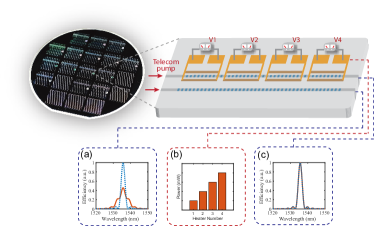
Figure 1 presents a conceptual schematic of a wafer-scale nonlinear photonic platform based on TF-PPLN waveguides integrated with segmented TO tuning modules. Without micro-heaters, the QPM spectra of TF-PPLN waveguides typically see broadened or multi-peak profiles due to variations in film thickness and other geometric parameters (e.g., etching depth or top width), as shown in Fig. 1(a). By individually controlling the thermal power applied to each micro-heater [Fig. 1(b)], we can precisely adjust and align the QPM peaks to converge on the desired target peak wavelength, as shown in Fig. 1(c). The segmented micro-heaters essentially fine tune the effective film thickness in each section to enhance the global flatness of the TF-PPLN chip. Under this circumstance, the peak conversion efficiency of the PPLN waveguides could be recovered to approach the ideal level, depending on the remaining un-compensated film thickness variations.
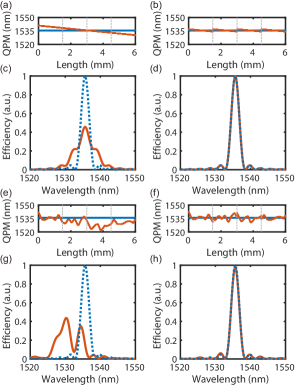
To validate our concept, we simulate the QPM spectra with thickness variation and those after optimized local thermal tuning, as illustrated in Fig. 2. Here we consider two scenarios: i) a hypothetical scenario where the film thickness linearly increases from the input to the output port; ii) a realistic scenario based on actually mapped thickness data from our recent research. In the first case, the film thickness linearly increases from 600nm to 602nm over a 6-mm device length, which corresponds to a linearly chirped peak QPM wavelength from 1529nm to 1541nm, as shown in Fig. 2(a). This leads to significant degradation in the peak conversion efficiency and deviation from the ideal QPM spectrum [Fig. 2(c), blue dashed curve denotes the ideal spectrum]. However, when we equip this inhomogeneously broadened TF-PPLN waveguide with four segmented TO tuning modules that align the center QPM wavelengths in each section [Fig. 2(b)], the normalized conversion efficiency is restored to 98 of the ideal value with a nearly perfect QPM spectrum, as shown in Fig. 2(d). To investigate the performance of our segmented tuning scheme in a more realistic scenario (second case), we use the mapped thickness data from our previous study [Fig. 2(e)] [17], which lead to a multi-peak QPM spectrum with a peak conversion efficiency 45.2 of the ideal case [Fig. 2(g)]. Similar to the first case, by aligning the local effective film thickness using micro-heaters, the normalized conversion efficiency could be enhanced by a factor of 2.2, to 97 of the ideal case, as shown in Fig. 2(h). Moreover, the QPM spectrum is successfully recovered to a single main peak with a standard sinc profile.
III DEVICE FABRICATION AND CHARACTERIZATION
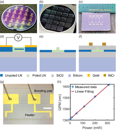
We perform wafer-scale fabrication of the TF-PPLN devices using a process detailed in Fig. 3. The device is fabricated on a commercial 4-inch LNOI wafer supplied by NANOLN Ltd., comprising a 600nm MgO-doped LN thin-film layer, a 2µm oxide buffer layer, and a 500µm silicon substrate. Firstly, the poling finger electrodes are patterned using an i-line UV stepper lithography (ASML), followed by thermal evaporation of nichrome (NiCr) and gold (Au) and a standard lift-off process, as shown in Fig. 3(a). Secondly, we employ a home-built automated probe station that is programmable to precisely position the probes on the poling electrodes sequentially and apply the necessary poling voltage pulses [35, 36, 37]. This automation facilitates the reliable periodic poling of an entire 1.5 cm × 1.5 cm die without manual control or intervention, significantly reducing the workload of wafer-scale periodic poling. Thirdly, after removal of all metal electrodes, a second aligned stepper lithography is carried out to define the patterns of optical waveguides in the poled regions. The exposed photoresist patterns are then transferred to the LN layer using a reactive ion etching (RIE) process [Fig. 3(b)]. Subsequently, the fabricated TF-PPLN waveguides are cladded in silicon dioxide (SiO2) using a plasma-enhanced chemical vapor deposition (PECVD) system. Fourthly, another two aligned photolithography processes are employed to fabricate the NiCr heaters in the vicinity of the optical waveguides, as well as the Au electrodes and bonding pads for wire bonding, similar to the process described in Ref. [26]. Finally, the fabricated device undergoes cleaving and facet polishing to ensure good end-fire optical coupling. The Au electrode pads, consisting of 4 or 8 pairs of anodes and cathodes, are wire-bonded to a printed circuit board (PCB) to facilitate independent control of each segmented micro-heater [Fig. 3(c)]. The full device fabrication flow is illustrated in the cross-sectional schematics in Fig. 3(d)-(f). Figure 3(g) shows a close-up microscope image of the fabricated segmented micro-heaters. To evaluate the tuning efficiency of our segmented micro-heaters, uniformly increasing DC currents are applied simultaneously to all electrodes. As depicted in Fig. 3(h), the peak QPM wavelength exhibits a red shift in response to the incremental heating power, which indicates a thermal tuning efficiency of 50 pm/mW, which could be further improved by reducing the thermal power leakage using a suspended structure [26].
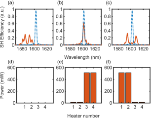
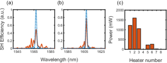
Finally, we demonstrate the effective recovery of distorted QPM spectra using our segmented TO tuning modules, as shown in Figs. 4-5. The TF-PPLN devices follow a similar design to our previous work [2], targeting SHG from telecom to near-visible bands. A telecom tunable light source (Santec TSL-550) is coupled into and out of the fabricated devices utilizing two optical lensed fibers. A fiber polarization controller is used to maintain a fundamental transverse-electric (TE) mode input. The measured SHG efficiency as a function of pump wavelength, also known as the QPM spectrum, is acquired by sweeping the input wavelength and simultaneously recording the output SHG power using a visible-band photodetector (Newport 1801). For a 6mm long device in Fig. 4(a), the QPM profile without thermal tuning features four main peaks, including two dominant ones at 1585 nm and 1593 nm. The peak conversion efficiency clearly falls short of the theoretical optimum ( 29.6 compared with ideal QPM peak, blue dashed curve) due to the inhomogeneous broadening of the QPM spectrum. We subsequently apply DC currents to the 4 segmented micro-heaters integrated with this TF-PPLN waveguide, and by monitoring the QPM spectra, fine-tune the heating powers to re-align the scattered QPM peaks. After a few iterations, we achieve an optimized set of tuning powers for the micro-heaters [Fig. 4(e)], leading to a single-peak QPM spectrum as depicted in Fig. 4(b). The measured peak SH conversion efficiency is increased by 108 from the un-optimized value, which corresponds to 61.7 of the ideal scenario. Moreover, it is also feasible to further re-shape the QPM spectra by applying another set of tuning currents, as exhibited in Fig. 4(c).
We further fabricate and test a 1cm long TF-PPLN optical waveguide with 8 segmented micro-heaters, which ideally features a higher absolute conversion efficiency but is more prone to film thickness variations. As shown in Fig. 5(a), before the thermal tuning of micro-heaters, the QPM spectrum exhibits many unwanted sidelobes, which degrades the SHG conversion efficiency from the ideal value. Similar to the case above, by applying appropriate DC powers [as indicated in Fig. 5(c)], we achieved a 57 enhancement of peak SH conversion efficiency, with significantly suppressed sidelobes, as the measured QPM spectrum in Fig. 5(b) shows. By carefully calibrating the visible and telecom coupling losses of the chip, we estimate an on-chip SHG efficiency of 1153 for the device with optimized thermal tuning parameters (734 before tuning).
IV CONCLUSIONS
In conclusion, we have demonstrated the wafer-scale production of TF-PPLN optical waveguides leveraging UV stepper lithography and an automated poling probe station. We address the degradation of conversion efficiency due to inhomogeneous film thickness by employing a segmented thermal tuning scheme. We show the successful recovery of single-peak QPM spectral profiles with up to 108 enhancement of the peak conversion efficiency without the need of pre-fabrication thickness mapping or design compensation, which is highly appealing for high-volume and low-cost wafer-scale production. The thermal tuning efficiency can be further enhanced by incorporating local air trenches to minimize heat leakage [26]. Even higher peak conversion efficiencies and better QPM spectral shapes could be achieved by implementing more thermal tuning modules and an automated control algorithm for optimizing the tuning parameters. This will enable faster searching for optimal working points, simultaneous control over multiple TF-PPLN devices, and real-time adaptation to environmental drifts. The scalable fabrication and tuning methodologies presented in this work mark an important step towards future large-scale nonlinear photonic integrated circuits with high efficiencies, versatile functionalities, and excellent reconfigurability, unlocking new opportunities for future quantum and classical photonic applications.
Acknowledgements.
The author would like to thank Dr. Wing-Han Wong, Mr. Hanke FENG, and Dr. Baojie CHEN for his kind help and guidance in the fabrication process. This work is supported by Research Grants Council, University Grants Committee (CityU 11204820, NCityU113/20); Croucher Foundation (9509005). Xiaoting Li acknowledge support form Hong Kong PhD Fellowship Scheme (PF18-17958). The authors declare no conflicts of interest.References
- Boes et al. [2023] A. Boes, L. Chang, C. Langrock, M. Yu, M. Zhang, Q. Lin, M. Lončar, M. Fejer, J. Bowers, and A. Mitchell, Lithium niobate photonics: Unlocking the electromagnetic spectrum, Science 379, eabj4396 (2023).
- Wang et al. [2018a] C. Wang, C. Langrock, A. Marandi, M. Jankowski, M. Zhang, B. Desiatov, M. M. Fejer, and M. Lončar, Ultrahigh-efficiency wavelength conversion in nanophotonic periodically poled lithium niobate waveguides, Optica 5, 1438 (2018a).
- Zhao et al. [2020a] J. Zhao, M. Rüsing, U. A. Javid, J. Ling, M. Li, Q. Lin, and S. Mookherjea, Shallow-etched thin-film lithium niobate waveguides for highly-efficient second-harmonic generation, Optics Express 28, 19669 (2020a).
- Rao et al. [2019] A. Rao, K. Abdelsalam, T. Sjaardema, A. Honardoost, G. F. Camacho-Gonzalez, and S. Fathpour, Actively-monitored periodic-poling in thin-film lithium niobate photonic waveguides with ultrahigh nonlinear conversion efficiency of 4600 %W -1 cm -2, Optics Express 27, 25920 (2019).
- Lu et al. [2019] J. Lu, J. B. Surya, X. Liu, A. W. Bruch, Z. Gong, Y. Xu, and H. X. Tang, Periodically poled thin-film lithium niobate microring resonators with a second-harmonic generation efficiency of 250,000%/W, Optica 6, 1455 (2019).
- Chen et al. [2019] J.-Y. Chen, Z.-H. Ma, Y. M. Sua, Z. Li, C. Tang, and Y.-P. Huang, Ultra-efficient frequency conversion in quasi-phase-matched lithium niobate microrings, Optica 6, 1244 (2019).
- Ledezma et al. [2022] L. Ledezma, R. Sekine, Q. Guo, R. Nehra, S. Jahani, and A. Marandi, Intense optical parametric amplification in dispersion-engineered nanophotonic lithium niobate waveguides, Optica 9, 303 (2022).
- Jankowski et al. [2022] M. Jankowski, N. Jornod, C. Langrock, B. Desiatov, A. Marandi, M. Lončar, and M. M. Fejer, Quasi-static optical parametric amplification, Optica 9, 273 (2022).
- Zhao et al. [2020b] J. Zhao, C. Ma, M. Rüsing, and S. Mookherjea, High Quality Entangled Photon Pair Generation in Periodically Poled Thin-Film Lithium Niobate Waveguides, Physical Review Letters 124, 163603 (2020b).
- Xue et al. [2021a] G.-T. Xue, X.-H. Tian, C. Zhang, Z. Xie, P. Xu, Y.-X. Gong, and S.-N. Zhu, Effect of thickness variations of lithium niobate on insulator waveguide on the frequency spectrum of spontaneous parametric down-conversion*, Chinese Physics B 30, 110313 (2021a).
- Wang et al. [2018b] C. Wang, M. Zhang, X. Chen, M. Bertrand, A. Shams-Ansari, S. Chandrasekhar, P. Winzer, and M. Lončar, Integrated lithium niobate electro-optic modulators operating at CMOS-compatible voltages, Nature 562, 101 (2018b).
- He et al. [2019a] M. He, M. Xu, Y. Ren, J. Jian, Z. Ruan, Y. Xu, S. Gao, S. Sun, X. Wen, L. Zhou, L. Liu, C. Guo, H. Chen, S. Yu, L. Liu, and X. Cai, High-performance hybrid silicon and lithium niobate Mach–Zehnder modulators for 100 Gbit s-1 and beyond, Nature Photonics 13, 359 (2019a).
- Wan et al. [2022] L. Wan, Z. Yang, W. Zhou, M. Wen, T. Feng, S. Zeng, D. Liu, H. Li, J. Pan, N. Zhu, W. Liu, and Z. Li, Highly efficient acousto-optic modulation using nonsuspended thin-film lithium niobate-chalcogenide hybrid waveguides, Light: Science & Applications 11, 145 (2022).
- Wang et al. [2019] C. Wang, M. Zhang, M. Yu, R. Zhu, H. Hu, and M. Loncar, Monolithic lithium niobate photonic circuits for Kerr frequency comb generation and modulation, Nature Communications 10, 978 (2019).
- He et al. [2019b] Y. He, Q.-F. Yang, J. Ling, R. Luo, H. Liang, M. Li, B. Shen, H. Wang, K. Vahala, and Q. Lin, Self-starting bi-chromatic LiNbO 3 soliton microcomb, Optica 6, 1138 (2019b).
- Bruch et al. [2021] A. W. Bruch, X. Liu, Z. Gong, J. B. Surya, M. Li, C.-L. Zou, and H. X. Tang, Pockels soliton microcomb, Nature Photonics 15, 21 (2021).
- Op De Beeck et al. [2021] C. Op De Beeck, F. M. Mayor, S. Cuyvers, S. Poelman, J. F. Herrmann, O. Atalar, T. P. McKenna, B. Haq, W. Jiang, J. D. Witmer, G. Roelkens, A. H. Safavi-Naeini, R. Van Laer, and B. Kuyken, III/V-on-lithium niobate amplifiers and lasers, Optica 8, 1288 (2021).
- Desiatov and Lončar [2019] B. Desiatov and M. Lončar, Silicon photodetector for integrated lithium niobate photonics, Applied Physics Letters 115, 121108 (2019).
- Guo et al. [2022a] X. Guo, L. Shao, L. He, K. Luke, J. Morgan, K. Sun, J. Gao, T.-C. Tzu, Y. Shen, D. Chen, B. Guo, F. Yu, Q. Yu, M. Jafari, M. Lončar, M. Zhang, and A. Beling, High-performance modified uni-traveling carrier photodiode integrated on a thin-film lithium niobate platform, Photonics Research 10, 1338 (2022a).
- Zhu et al. [2023] S. Zhu, Y. Zhang, Y. Ren, Y. Wang, K. Zhai, H. Feng, Y. Jin, Z. Lin, J. Feng, S. Li, Q. Yang, N. H. Zhu, E. Y.-B. Pun, and C. Wang, Waveguide-Integrated Two-Dimensional Material Photodetectors in Thin-Film Lithium Niobate, Advanced Photonics Research 4, 2300045 (2023).
- Nehra et al. [2022] R. Nehra, R. Sekine, L. Ledezma, Q. Guo, R. M. Gray, A. Roy, and A. Marandi, Few-cycle vacuum squeezing in nanophotonics, Science 377, 1333 (2022).
- Stokowski et al. [2023] H. S. Stokowski, T. P. McKenna, T. Park, A. Y. Hwang, D. J. Dean, O. T. Celik, V. Ansari, M. M. Fejer, and A. H. Safavi-Naeini, Integrated quantum optical phase sensor in thin film lithium niobate, Nature Communications 14, 3355 (2023).
- Guo et al. [2022b] Q. Guo, R. Sekine, L. Ledezma, R. Nehra, D. J. Dean, A. Roy, R. M. Gray, S. Jahani, and A. Marandi, Femtojoule femtosecond all-optical switching in lithium niobate nanophotonics, Nature Photonics 16, 625 (2022b).
- Ledezma et al. [2023] L. Ledezma, A. Roy, L. Costa, R. Sekine, R. Gray, Q. Guo, R. Nehra, R. M. Briggs, and A. Marandi, Octave-spanning tunable infrared parametric oscillators in nanophotonics, Science Advances 9, eadf9711 (2023).
- Li et al. [2022] M. Li, L. Chang, L. Wu, J. Staffa, J. Ling, U. A. Javid, S. Xue, Y. He, R. Lopez-rios, T. J. Morin, H. Wang, B. Shen, S. Zeng, L. Zhu, K. J. Vahala, J. E. Bowers, and Q. Lin, Integrated Pockels laser, Nature Communications 13, 5344 (2022).
- Liu et al. [2022] X. Liu, C. Zhang, Y. Pan, R. Ma, X. Zhang, M. Chen, L. Liu, Z. Xie, S. Zhu, S. Yu, and X. Cai, Thermally tunable and efficient second-harmonic generation on thin-film lithium niobate with integrated micro-heater, Optics Letters 47, 4921 (2022).
- Luke et al. [2020] K. Luke, P. Kharel, C. Reimer, L. He, M. Loncar, and M. Zhang, Wafer-scale low-loss lithium niobate photonic integrated circuits, Optics Express 28, 24452 (2020).
- Fejer et al. [1992] M. Fejer, G. Magel, D. Jundt, and R. Byer, Quasi-phase-matched second harmonic generation: Tuning and tolerances, IEEE Journal of Quantum Electronics 28, 2631 (Nov./1992).
- Tian et al. [2021] X.-H. Tian, W. Zhou, K.-Q. Ren, C. Zhang, X. Liu, G.-T. Xue, J.-C. Duan, X. Cai, X. Hu, Y.-X. Gong, Z. Xie, and S.-N. Zhu, Effect of dimension variation for second-harmonic generation in lithium niobate on insulator waveguide [Invited], Chinese Optics Letters 19, 060015 (2021).
- Xue et al. [2021b] G.-T. Xue, Y.-F. Niu, X. Liu, J.-C. Duan, W. Chen, Y. Pan, K. Jia, X. Wang, H.-Y. Liu, Y. Zhang, P. Xu, G. Zhao, X. Cai, Y.-X. Gong, X. Hu, Z. Xie, and S. Zhu, Ultrabright Multiplexed Energy-Time-Entangled Photon Generation from Lithium Niobate on Insulator Chip, Physical Review Applied 15, 064059 (2021b).
- Santandrea et al. [2019] M. Santandrea, M. Stefszky, G. Roeland, and C. Silberhorn, Characterisation of fabrication inhomogeneities in Ti:LiNbO 3 waveguides, New Journal of Physics 21, 123005 (2019).
- Zhao et al. [2023] J. Zhao, X. Li, T.-C. Hu, A. A. Sayem, H. Li, A. Tate, K. Kim, R. Kopf, P. Sanjari, M. Earnshaw, N. K. Fontaine, C. Wang, and A. Blanco-Redondo, Unveiling the origins of quasi-phase matching spectral imperfections in thin-film lithium niobate frequency doublers, APL Photonics 8, 126106 (2023).
- Kuo [2022] P. S. Kuo, Noncritical phasematching behavior in thin-film lithium niobate frequency converters, Optics Letters 47, 54 (2022).
- Chen et al. [2023] P.-K. Chen, I. Briggs, C. Cui, L. Zhang, M. Shah, and L. Fan, Adapted poling to break the nonlinear efficiency limit in nanophotonic lithium niobate waveguides, Nature Nanotechnology 10.1038/s41565-023-01525-w (2023).
- Zhao et al. [2019] J. Zhao, M. Rüsing, and S. Mookherjea, Optical diagnostic methods for monitoring the poling of thin-film lithium niobate waveguides, Optics Express 27, 12025 (2019).
- Nagy and Reano [2020] J. T. Nagy and R. M. Reano, Submicrometer periodic poling of lithium niobate thin films with bipolar preconditioning pulses, Optical Materials Express 10, 1911 (2020).
- Niu et al. [2020] Y. Niu, C. Lin, X. Liu, Y. Chen, X. Hu, Y. Zhang, X. Cai, Y.-X. Gong, Z. Xie, and S. Zhu, Optimizing the efficiency of a periodically poled LNOI waveguide using in situ monitoring of the ferroelectric domains, Applied Physics Letters 116, 101104 (2020).