Reducing strain fluctuations in quantum dot devices by gate-layer stacking
Abstract
Nanofabricated metal gate electrodes are commonly used to confine and control electrons in electrostatically defined quantum dots. However, these same gates impart a complicated strain pattern that affects the confinement potential and potentially impairs device functionality. Here we investigate strain-induced fluctuations of the potential energy in Si/SiGe heterostructures, caused by (i) lattice mismatch, (ii) materials-dependent thermal contraction, and (iii) depositional stress in the metal gates. By simulating different gate geometries, ranging from simple to realistically complicated, and including features like overlapping metal and oxide layers, we can explain most observed strain features. In particular, we show that strain-induced potential fluctuations can be suppressed by employing overlapping gates that cover the whole active region, when the oxide layers are thin. These results suggest that strain effects should not present a serious challenge to qubit uniformity when following simple design rules.
I Introduction
Gate-defined quantum dots in Si/SiGe quantum wells are a promising platform for large-scale quantum computation [1, 2, 3], where recent demonstrations of single and two qubit gates have exceeded error correction thresholds [4, 5, 6]. While these achievements represent important milestones, useful quantum hardware will require vast arrays of reliable, low-error qubits. Scaling up will require a level of qubit reproducibility and uniformity on par with transistors in modern integrated circuits [7, 8]. Such uniformity has been achieved for certain dot properties like orbital and charging energies [9], but remains a challenge for properties like the valley energy splitting [10], due to the inherent atomistic disorder of the SiGe random alloy [11, 12]. Some types of non-uniformity are potentially reconfigurable, such as interfacial trapped charge [13, 14], which can modify the local electrostatics [15] and cause the formation of unintentional quantum dots [16, 17, 18]. Other sources of variability (e.g., valley splitting) are immutable, and are prescribed during heterostructure growth or device fabrication.
Local strain fields can significantly affect the in-plane confinement potential of quantum dots [19, 20]. These strains arise from the structural or geometrical features of a device, such as metal electrodes or etched regions, which are intentionally patterned atop the quantum well that houses the qubits 111Strain fluctuations also arise from misfit locations in plastically relaxed virtual substrates [39]; however, we do not consider such effects here.. Such structures are carefully designed to provide electrostatic control of the qubit environment. However, the strains arising from these gates can have a very different effect on the confinement potential than the intended one, resulting in energy variations on the order of meV [22, 23], which is comparable to the electrostatic confinement. Such fluctuations can cause unintentional quantum dots [19], and can affect exchange interactions between electrons in neighboring dots [3, 24, 25, 26]. Despite such compelling arguments to treat the strain and electrostatics on equal footing, this is seldom done in experiments or simulations.
In this work, we numerically investigate strain effects arising from three main sources: (i) lattice mismatch between the Si in the quantum well and the SiGe alloy of the barriers [27], (ii) unequal contractions of different materials as the device is cooled [19], and (iii) depositional stress, which occurs in a metal when it is deposited on a semiconductor or an oxide [28]. These strain calculations are used to estimate conduction-band energies in the Si quantum well, as explained in Methods, from which we deduce the locally varying confinement potential. (In Supplementary Fig. S3, we also include the corresponding electrostatic potential.) Beginning with simple gate structures, we work our way up to realistic devices measured in qubit experiments [29, 30]. Due to the long-range nature of the strain fields, our simulations exhibit both short-range variations that mirror the locally varying gate structure, as well as smoother, averaged behavior arising from multiple gates, which is manifested (for example) as edge effects.
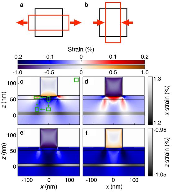
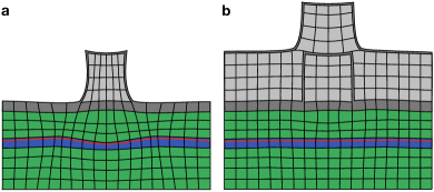
By exploring gate designs commonly used in experiments, we can draw some practical conclusions for designing future experiments. Most notably, we find that undesirable strain fluctuations can be greatly suppressed by tightly stacking multiple layers of gates. To illustrate this point, in Fig. 1a, we depict the strong, locally varying strain found in the plane of the quantum well, directly below an isolated, narrow gate. In contrast, it is clear that a wide gate will produce a relatively uniform strain in the quantum well below, except near the edges of the gate. Now if we consider several closely space gates, or an overlapping geometry like the one shown in Fig. 1b, the strain will be nearly uniform, similar to the situation for a wide gate. We note that this result cannot hold for a thick oxide layer, because the overlapping gate will be too far away to have an effect, resulting in a strain response more similar to Fig. 1a. We also observe more subtle behaviors from gate stacking, including a change of sign in the strain (for the cases of individual, overlapping gates vs a global gate), and the formation of a double-well (or double-barrier) feature on either side of a wire. In the following discussion, we elaborate on these and other phenomena, and provide additional numerical details.
II Results
To study the physics of strain fluctuations under top gates, and particularly, the effect of gate-layer stacking, we simulate four systems of varying complexity. The first system consists of a long metal gate fabricated atop an otherwise uniform Si/SiGe heterostructure, as shown in Fig. 2, which serves as a minimal model for describing the effects of local strain. The second system considers the effects of several closely spaced gates, with or without a narrow crossing gate, as shown in Fig. 3. Figures 4 and 5 correspond to the experimental devices in Refs. [29] and [30], respectively. Here, the effects of gate-layer stacking are studied by including different subsets of overlapping gates in the simulations. Figure 5 also demonstrates the importance of oxide-layer thickness. All results shown here make use of the Solid Mechanics module of COMSOL Multiphysics [31], as described in Methods. The simulations incorporate all three sources of strain described above, with the materials parameters described in Methods. For the thermal contraction simulations, we assume the devices are cooled from to .
II.1 Single wire
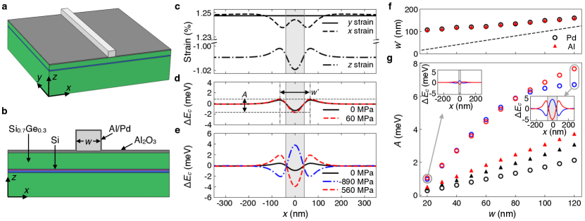
We first consider the simple wire geometry shown in Fig. 2a, where the wire is uniform along the direction. The corresponding cross section is shown in Fig. 2b. From bottom to top, the heterostructure in our simulations consists of a 2 m layer of strain-relaxed SiGe, a 9 nm Si quantum well, another 30 nm spacer layer of SiGe, and a 10 nm insulating layer of Al2O3. We assume that all interfaces in this structure are grown epitaxially, and that the quantum well is fully strained. The Si layer therefore experiences biaxial tensile strain due to the larger bulk lattice constant of SiGe. Except where noted (Fig. 5), we use this same heterostructure in all simulations reported below. Moreover the strain, and the energy variations it causes, are always evaluated in the plane of the two-dimensional electron gas (2DEG), which we take to lie 1.5 nm below the top quantum-well interface.
We first simulate just the heterostructure geometry, without any top gate. Here, the strain is caused by a combination of lattice mismatch and thermal contraction, giving the following diagonal strain results in the plane of the 2DEG: and . The strain causes an energy shift of the conduction band, as described in Methods, which accounts (in part) for the vertical confinement potential of the quantum well. We take as a reference point the conduction-band minimum at a point far away from the region of interest. Since the strain and the conduction-band minimum are both uniform in this geometry, the energy shift compared to the reference point, , is zero across the whole sample.
For the wire geometry of Figs. 2a and 2b, we consider an Al metal wire formed directly atop the oxide layer as shown, with a fixed height of 60 nm and a variable width . The wire causes local strain fluctuations, due to a combination of depositional stress and thermal contractions, with results shown in Fig. 2c. Here all three diagonal strain-tensor components are plotted (, , and ). The corresponding conduction-band energy shifts are shown in Fig. 2d, for cases with and without depositional stress, as indicated. Similarly, Fig. 2e shows results for a Pd wire. In this case, different values (and signs) of the depositional stress are reported in the literature; we therefore consider two different values, as well the case of no depositional stress. (The latter results differ from those in the Al wire because of the different thermal contractions.) For both sets of simulations, the energy shift converges to its asymptotic value far from the wire, such that . Near the gates, has strong variations on the scale of several meV. For the Al wire, the depositional stress is low, and we see that its contribution to is small. For the Pd wire, the opposite is true, and the depositional stress is seen to dominate over the thermal stress. Here, changes sign for the case of depositional tensile stress () vs compressive stress (). Supplementary Fig. S1 provides further insight into the specific shape of the strain profiles.
The dependence of strain effects on wire width is shown in Figs. 2f and 2g. We now introduce two parameters to characterize the variations, as defined in Fig. 2d: the peak-to-peak width and the trough-to-peak amplitude . These two parameters are plotted in Figs. 2f and 2g, respectively. The width parameter is found to be essentially universal, with no significant dependence on materials or strain parameters. Interestingly, asymptotes to a nonzero value for small , and to (with ), for large . Both effects can be understood in terms of an approximate “45∘ rule,” in which the strain fields extend out at an angle from the gates, with details depending slightly on the wire width. We note that there is no contradiction that remains nonzero as , since also in this limit. However, there is an interesting dependence of on the strain parameters and on . We see that initially follows a linear dependence on in all cases. For the case of the red and blue circle data, this behavior changes at around -90 nm, where begins to plateau as the two edges of the wire no longer affect each other’s local strain field. Such plateaus are generally expected for large .
II.2 Parallel wires
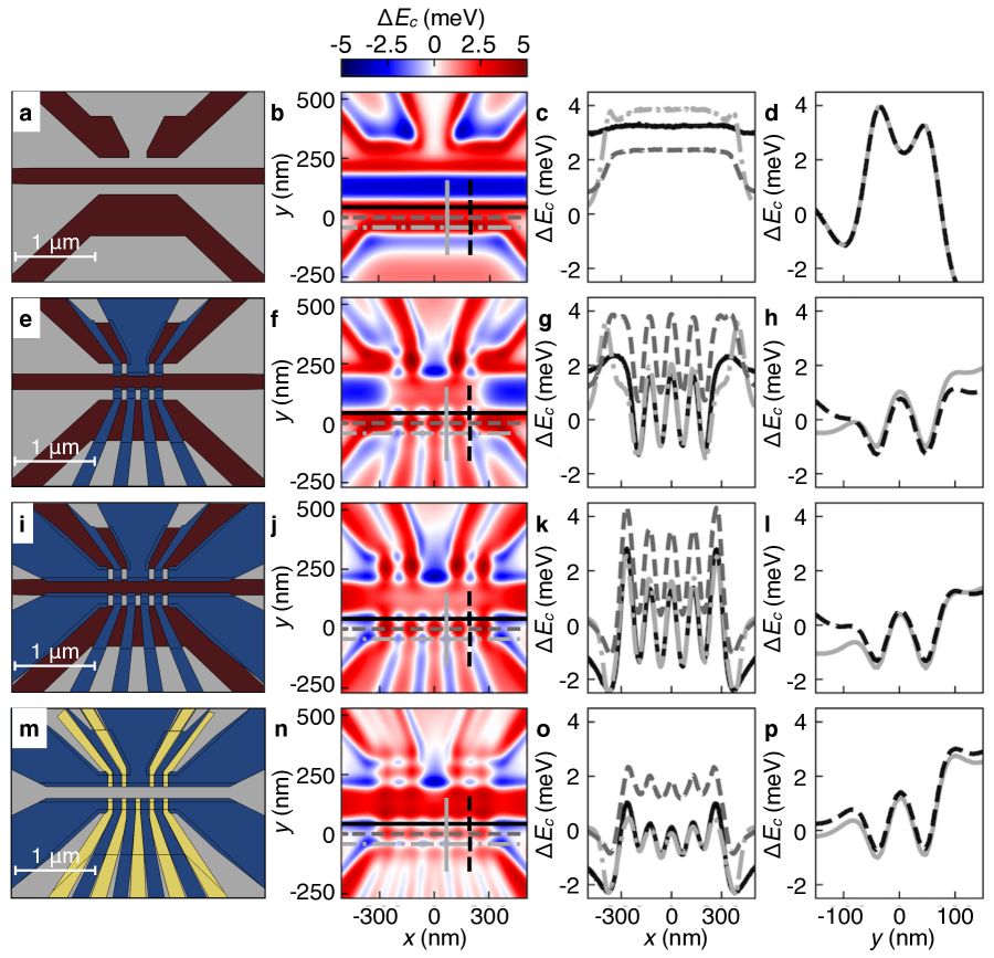
We now study how the single-wire picture is modified in the presence of additional wires, spaced closely enough that their strain fields overlap. We consider the geometries shown in Figs. 3a and 3b, comprising five parallel Al wires of width and height , with gaps of between the wires, representing a typical gate pitch for quantum-dot qubits [29]. In addition to these five gates, the first device also includes a crossing gate with the same cross-section dimensions, oriented perpendicular to the wires and separated from those wires by a 2 nm insulating layer of Al2O3. The second device has a gap in place of the crossing gate, but also includes a 2 nm conformal oxide layer covering the whole surface. All the wires in these simulations are taken to be very long, to suppress potential edge effects. The strains are computed, as described above, and the resulting conduction-band minima are plotted as a function of lateral position in Figs. 3c and 3d. Several cuts are taken in the plane of the 2DEG, along the indicated lines, yielding the results shown in Figs. 3e and 3f.
In these multigate devices, exhibits short-range variations that mirror the local gate structure, and a slowly varying envelope arising from long-range strain fields. differs in interesting ways for the two geometries, especially near the crossing regions (). The trough-to-peak amplitudes are similar to those observed in Fig. 2, indicating that the short-range features are mainly governed by the gate structure right above the 2DEG. It is important to note that the amplitudes of these oscillations are large enough to produce unintentional dots. For example, the series of dips along the gray dashed line in Fig. 3d are 3 meV deep, compared to orbital excitation energies of 1-3 meV in typical dots. Such potential fluctuations are also large enough to affect exchange interactions, which are used to construct two-qubit gates. For example, it has been shown that a useful exchange interaction of strength requires having a tunnel barrier between two Si/SiGe dots with a height less than 1 meV [3]. If necessary, such strain-induced variations could potentially be compensated electrostatically; however, for complicated gate geometries, the competition between short- and long-range strain features could make this challenging. A desirable approach is therefore to compensate some of the fluctuation through gate design, as discussed below. Finally, we note that the envelope of the potential variations can also vary by several meV, even across a series of identical wires. This is particularly evident in the dot-dashed linecuts of Figs. 3e and 3f, where the roughly 1 meV difference in between neighboring wires can be viewed as an effective detuning shift between quantum dots.
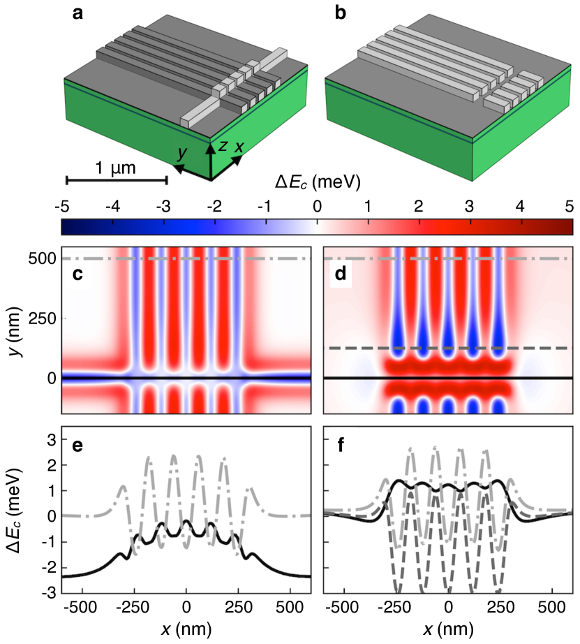
We now study the effect of overlapping gates in Fig. 3e by comparing results directly underneath the crossing gate (solid line) to those far away from the gate (dot-dashed line). While the envelopes of the two curves appear similar, the amplitudes of their short-range oscillations differ by a factor of six. Moreover, the oscillations are seen to have opposite sign.
One would like to understand and potentially predict such interesting behavior. Indeed, for simple geometries, with only a few materials layers (e.g., Fig. 2, or the dot-dashed line in Fig. 3c), this is often possible. However more-complicated geometries, particularly those with nontrivial three-dimensional (3D) features, can give rise to unexpected behavior, like the sign change of the short-range oscillations. In Methods, we note that is dominated by the component of the strain, , which depends on multiple factors, including locally varying interface profiles, the specific values of thermal expansion coefficients, and the various layer thicknesses. In fact, in Sec. II.4 below, we study a geometry where simply changing the oxide thickness, keeping everything else fixed, causes a similar sign change in the short-range oscillations. Notwithstanding these challenges, we can make some general observations. For example, in Fig. 3e, the oscillations change sign, moving from the dot-dashed to solid linecuts, indicating that a different linecut, placed somewhere between these two lines, should provide more-strongly suppressed oscillations. Similarly, modifying the gate geometry could also reduce the oscillation amplitude. For example, a narrower crossing gate, or more-closely spaced parallel gates could both produce the desired smoothing effect. These results demonstrate that gate-layer stacking can provide an effective strategy for reducing short-range strain variations.
An alternative scheme for suppressing short-range oscillations is simply to remove the top gates (solid line in Figs. 3d and 3f). In this case, the strain fields are mainly long-range, as desired; however, as a result, short-range electrostatic control is also sacrificed. While relatively smooth potentials can be achieved along the lines of both geometries in Fig. 3, we note that their qualitative behaviors differ. The dip features in along the gray dashed line in Fig. 3f are especially prominent, indicating that edge effects (e.g., caused by the terminal ends of wires) have a particularly strong effect on both short- and long-range behaviors.
II.3 Quadruple-quantum-dot device
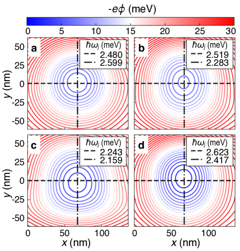
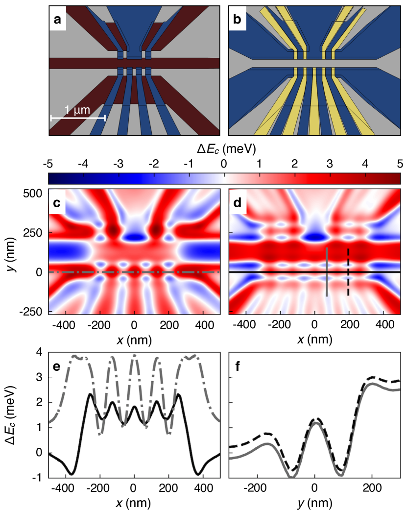
We now consider gate-layer stacking in realistic and commonly used overlapping gate geometries, like the quadruple quantum dot shown in Fig. 4 [29]. For the simulations, we assume the same heterostructure as in Fig. 2 — now with three overlapping layers of Al metal gates. From bottom to top, these correspond to screening gates (maroon), plunger or reservoir gates (blue), and tunnel-barrier gates (yellow). We also include 2 nm Al2O3 insulating layers between each of the metal layers. In the lower portion of the image, the plunger gates define four quantum dots and two 2DEG reservoirs, on either side of the dots. In the upper portion of the image, the plungers define two charge-sensing dots, surrounded by three 2DEG reservoirs. To avoid edge effects, we use a full simulation cell of size m2 in the - plane and 2 m in the direction. We have checked that this system size yields converged results.
To disentangle the effects of the different gate layers in our simulations, we begin with a smaller set of gates, and progressively add more gates until reaching a complete set. Figure 4 shows results for the geometries shown in panels a and b. Figure 4a includes only the screening, plunger, and upper-middle reservoir gates, while Fig. 4b includes all the gates. (Two intermediate gate sets are also considered in Supplementary Fig. S2.) The linecuts indicated in Figs. 4c and 4d are plotted in Figs. 4e and 4f. The effectiveness of gate-layer stacking is seen most clearly by comparing the horizontal lines in Figs. 4c and 4d. In Fig. 4c, this cut crosses just the four plunger gates, which are separated by gaps. In Fig. 4d, the gaps are all filled by overlapping tunnel-barrier gates, and reservoir gates are also present on either side, such that the whole cut is covered by metal. As consistent with Fig. 3, the case with gaps between the gates (dot-dashed line in Fig. 4e) has short-range oscillations of about 3 meV. Moreover, in the fully covered case (solid line), the short-range oscillations are suppressed by a factor of three. However, the oscillations have the same sign for these two geometries, in contrast with the results observed in Fig. 3d. A notable difference between these two devices is that the crossing gate in Fig. 3a covers the parallel gates globally, as opposed to the tunnel-barrier gates in Fig. 4b, which just fill in the gaps, locally, between the plunger gates.
The oscillation envelopes in Fig. 4e also show interesting behavior. We observe that neighboring dots can have confinement potentials of different depths, representing built-in, fixed detuning parameters on the order of 0.25-0.35 meV. Moreover, the envelopes for the two geometries have opposite curvature, which we attribute to the presence of side-reservoir gates for the full gate geometry. The different curvature signs suggest that alternative gate geometries could be used to reduce the detuning shifts, for example, by moving the side-reservoir gates further away from the dots.
Finally, we note that strain from the screening gates can have unexpected effects on quantum-dot confinement in the direction, as demonstrated in Fig. 4f. Here, the combination of screening and plunger gates produces a double-dip feature on either side of the dot, which is weakly affected by the presence of the tunnel-barrier or reservoir gates. The peak between the dips has the opposite sign as the electrostatic dot confinement. To estimate its effect, we fit the peak to the upside-down confinement potential , yielding a characteristic orbital energy of meV, where is the transverse effective mass of silicon. Comparing this with typical dot orbital energies of -3 meV (see Supplementary Fig. S3) suggests that the strain-induced effect is not likely to produce a double-dot along ; however, it can strongly affect the dot shape — effectively flattening and widening the bottom of the confinement potential. For weaker electrostatic confinements, the strain-induced effect will eventually dominate.
II.4 Effect of oxide-layer thickness
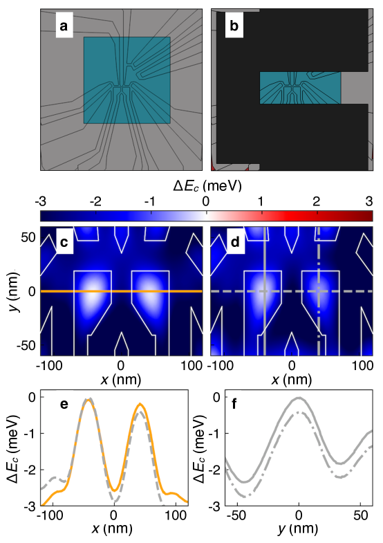
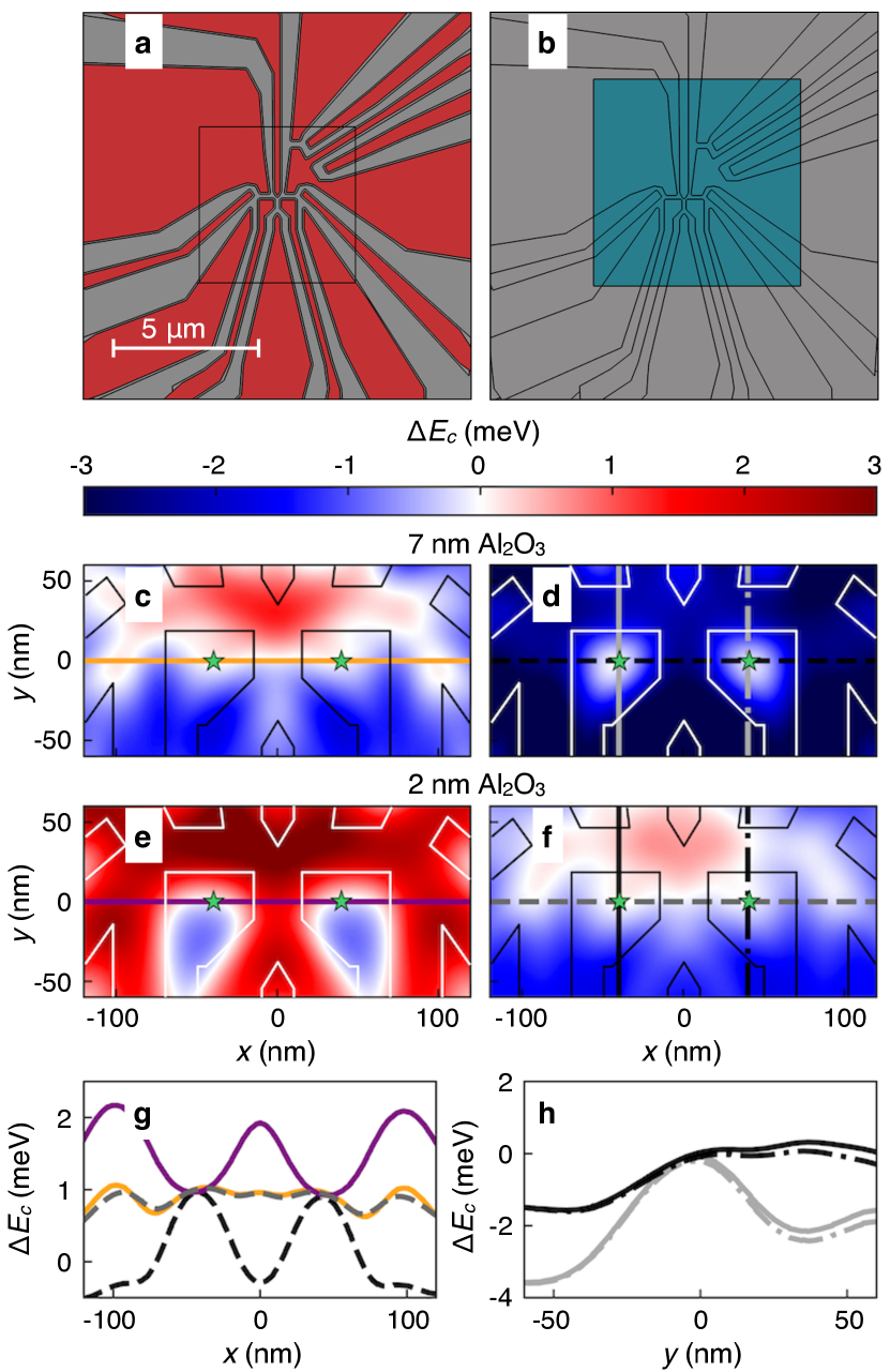
In the final set of simulations, we also study gate-layer stacking, while showing how using thicker oxides modifies our main conclusions. The device we consider is based on Ref. [30], with the two variations shown in Figs. 5a and 5b. Here, the heterostructure consists of a 1.2 m strain-relaxed Si0.7Ge0.3 buffer layer, an 8 nm Si quantum well, a 30 nm Si0.7Ge0.3 spacer, a 1 nm Si cap, a thin Al2O3 oxide layer, a 20 nm Al metal gate, and another thin Al2O3 layer. (We also consider the effect of an additional cobalt micromagnet layer in Supplementary Fig. S4.) To study the effects of oxide thickness, we consider two different cases: a 7 nm oxide layer (consistent with the device in [30]) and a 2 nm oxide layer (consistent with the device in [29]). This geometry is shown in Fig. 5a, while Fig. 5b also includes a 40 nm Al global gate. Results for are shown in Figs. 5c-5f, for the four different combinations of oxide thicknesses and gate geometries, with corresponding linecuts shown in Figs. 5g and 5h.
We begin by confirming the effect of gate-layer stacking, by comparing Figs. 5e and 5f. For these two simulations, the oxide thickness is the same as in the previous subsections (2 nm), and the only difference in the geometries is the global top gate. The linecut in Fig. 5g with no global top gate (solid-purple curve) shows strong short-range fluctuations, with similar amplitude and shape as previous simulations, while the stacked global gate (dashed-gray curve) has strongly suppressed fluctuations. A more surprising result is observed in the dashed-black linecut, which has the same accumulation-gate geometry, but a thicker (7 nm) oxide layer. Here, the short-range oscillations have the opposite sign compared to the solid-purple curve. This behavior is reminiscent of Fig. 3e; indeed, for both cases, the stacked gates responsible for this behavior cover the plungers globally. Interestingly, the amplitude of the oscillations for the thick-oxide device (dashed-black curve) is strongly enhanced compared to the thin-oxide device (dashed-gray curve), as if the thicker oxide were amplifying the oscillations. We attribute this behavior to 3D aspects of the gate geometry, whose effects are difficult to predict. For completeness, we also show results for a thick oxide with no global top gate (solid-orange curve), in which the oscillations are strongly suppressed, with features coincidentally similar to the gray-dashed curve.
Finally, in Fig. 5h, we consider linecuts along the axis that pass through the nominal centers of the quantum dots (green stars). Here, we consider only the full gate geometry, which includes the global top gate. Similar to linecuts along , these results confirm that stronger short-range fluctuations are obtained in the case of thicker oxides (gray curves). We also note the slight differences between results in the left- and right-hand dots in Fig. 5h (solid vs dashed curves), which are caused by long-range strain fields arising from the asymmetric top-gate configuration.
III Discussion
We have investigated local strain fluctuations in realistic Si/SiGe quantum dot devices, arising from inhomogeneous materials layers, and in particular, from the metal top gates. For these gates, we include effects from both thermal contraction and depositional stress, finding that the former dominates for Al gates, while the latter dominates for Pd gates. Focusing on Al gates, we note that strain along the axis () mainly determines the variations of the conduction-band minimum (), and is strongly affected by nontrivial 3D features such as the vertical layer stacking and the gate geometry, resulting in behavior that is not always intuitive.
Despite these challenges, we can draw some general conclusions. First, we note that exhibits both short-range variations that mirror the shape of the top gates, and long-range variations that produce slowly varying envelopes that modulate the fast oscillations. The amplitude of the short-range fluctuations is comparable, but often smaller, than typical electrostatic fluctuations produced by the top gates; however, unlike electrostatic fluctuations, strain-induced effects cannot be modified after fabrication. In some cases, the potential fluctuations can have a considerable effect on the shape of the dot, as in Figs. 4(g) and S3. Indeed, dot localization effects that were previously attributed to trapped charge [16, 17, 18] could potentially be explained, in full or in part, by strain effects. The long-range fluctuations cause potential shifts below neighboring plunger gates that act like built-in detuning potentials between the dots, which must be electrostatically compensated for proper gate operation.
The most important result reported in this work is that the tight stacking of gate layers provides a key tool for overcoming strain-induced potential fluctuations. Such stacked gates can be seen as largely reproducing the behavior of a uniform metal top gate. However, unexpected 3D effects can still occur, for example, when employing a thicker oxide layer between the metal gates, which can have the effect of amplifying the short-range potential fluctuations. Similarly, different styles of gate stacking can yield different potential profiles; for example, a globally spanning top gate (Fig. 5) is seen to cause very different behavior than local tunnel-barrier gates filling the gaps between plunger gates (Fig. 4), as evidenced by short-range oscillations with opposite signs.
In future work, as arrays of qubits are scaled up, and every aspect of qubit functionality is tightly controlled, it will be increasingly important to account for strain-induced confinement effects, which can compete with electrostatic confinement. The simplest approach to avoiding strain-induced behavior is to specifically design gate geometries to suppress these fluctuations. Clearly, gate-layer stacking is a key tool for such an approach. However, other design tools, such as modifying the lateral positions of gate electrodes, the thicknesses of oxide layers, or other 3D features of the gate geometry, could also serve this purpose. Generally, we anticipate that strain engineering will play an important role in future qubit technologies.
Methods
We calculate strain profiles using the Solid Mechanics module of COMSOL Multiphysics [31]. To perform these calculations, we must specify the Young’s modulus , Poisson’s ratio , and coefficients of thermal expansion (CTE) , for each material. Note that each of these parameters varies with temperature, although COMSOL assumes temperature-independent values. and depend only weakly on the temperature, so we simply adopt room-temperature values for these parameters, from the COMSOL parameter library. To account for the temperature dependence of the CTEs, we define temperature-averaged CTEs as , where and are the initial and final temperatures, respectively. We approximate these integrals using the temperature-dependent CTE data presented in Refs. [32, 33, 34, 35, 36, 37]. For the SiGe alloy, we use data for Si and Ge in combination with Vegard’s law to evaluate its CTE. The temperature-averaged CTEs are then given by . The biaxial strain from lattice mismatch is imposed through the initial-strain parameters and . Where specified, depositional stress in the metallic gates is imposed as an intrinsic stress. Finally, free boundary conditions [31] are enforced on every surface, except for the bottom surface, where we enforce contraction that matches the bulk thermal contraction of Si, to emulate the presence of a larger Si substrate.
The calculated strain profiles can then be related to the offsets of the conduction band in the Si quantum well by the relation [19]
| (1) |
where eV and eV are deformation potential coefficients [38], whose difference is a consequence of the anisotropy of the valleys, which are the low-energy points of the conduction band in momentum space for the strained Si/SiGe quantum well [2]. As a result, strain effects in are dominated by the component of the strain tensor, , as can be seen by comparing Figs. 2c and 2d. When computing energy fluctuations in Eq. (1), we use the strain evaluated in the 2DEG plane, which is assumed to lie below the top interface of the quantum well, where the low-energy electronic wave functions of the quantum well are concentrated. Finally, unless otherwise specified, is shifted in each calculation such that the asymptotic value of is zero, far away from the active region containing the gates.
Acknowledgments
We are grateful to Xiao Xue, Nodar Samkharadze, Gertjan Eenink, Menno Veldhorst, and Lieven Vandersypen for sharing device designs related to this work. We also thank Hudaiba Soomro for important clarifications related to the simulations. This research was sponsored in part by the Army Research Office under Awards No. W911NF-23-1-0110, W911NF-22-1-0090, and W911NF-17-1-0274. The views, conclusions, and recommendations contained in this document are those of the authors and are not necessarily endorsed by nor should they be interpreted as representing the official policies, either expressed or implied, of the Army Research Office or the U.S. Government. The U.S. Government is authorized to reproduce and distribute reprints for U.S. Government purposes notwithstanding any copyright notation herein.
References
- Loss and DiVincenzo [1998] D. Loss and D. P. DiVincenzo, Quantum computation with quantum dots, Phys. Rev. A 57, 120 (1998).
- Zwanenburg et al. [2013] F. A. Zwanenburg, A. S. Dzurak, A. Morello, M. Y. Simmons, L. C. L. Hollenberg, G. Klimeck, S. Rogge, S. N. Coppersmith, and M. A. Eriksson, Silicon quantum electronics, Rev. Mod. Phys. 85, 961 (2013).
- Burkard et al. [2023] G. Burkard, T. D. Ladd, A. Pan, J. M. Nichol, and J. R. Petta, Semiconductor spin qubits, Rev. Mod. Phys. 95, 025003 (2023).
- Xue et al. [2022] X. Xue, M. Russ, N. Samkharadze, B. Undseth, A. Sammak, G. Scappucci, and L. M. K. Vandersypen, Quantum logic with spin qubits crossing the surface code threshold, Nature 601, 343 (2022).
- Noiri et al. [2022] A. Noiri, K. Takeda, T. Nakajima, T. Kobayashi, A. Sammak, G. Scappucci, and S. Tarucha, Fast universal quantum gate above the fault-tolerance threshold in silicon, Nature 601, 338 (2022).
- Mills et al. [2022] A. R. Mills, C. R. Guinn, M. J. Gullans, A. J. Sigillito, M. M. Feldman, E. Nielsen, and J. R. Petta, Two-qubit silicon quantum processor with operation fidelity exceeding 99%, Science Advances 8, eabn5130 (2022).
- Zwerver et al. [2022] A. M. J. Zwerver, T. Krähenmann, T. F. Watson, L. Lampert, H. C. George, R. Pillarisetty, S. A. Bojarski, P. Amin, S. V. Amitonov, J. M. Boter, R. Caudillo, D. Correas-Serrano, J. P. Dehollain, G. Droulers, E. M. Henry, R. Kotlyar, M. Lodari, F. Lüthi, D. J. Michalak, B. K. Mueller, S. Neyens, J. Roberts, N. Samkharadze, G. Zheng, O. K. Zietz, G. Scappucci, M. Veldhorst, L. M. K. Vandersypen, and J. S. Clarke, Qubits made by advanced semiconductor manufacturing, Nature Electronics 5, 184 (2022).
- Meyer et al. [2023a] M. Meyer, C. Déprez, T. R. van Abswoude, I. N. Meijer, D. Liu, C.-A. Wang, S. Karwal, S. Oosterhout, F. Borsoi, A. Sammak, N. W. Hendrickx, G. Scappucci, and M. Veldhorst, Electrical control of uniformity in quantum dot devices, Nano Letters 23, 2522 (2023a).
- Zajac et al. [2016] D. M. Zajac, T. M. Hazard, X. Mi, E. Nielsen, and J. R. Petta, Scalable gate architecture for a one-dimensional array of semiconductor spin qubits, Phys. Rev. Appl. 6, 054013 (2016).
- Chen et al. [2021] E. H. Chen, K. Raach, A. Pan, A. A. Kiselev, E. Acuna, J. Z. Blumoff, T. Brecht, M. D. Choi, W. Ha, D. R. Hulbert, M. P. Jura, T. E. Keating, R. Noah, B. Sun, B. J. Thomas, M. G. Borselli, C. Jackson, M. T. Rakher, and R. S. Ross, Detuning axis pulsed spectroscopy of valley-orbital states in /- quantum dots, Phys. Rev. Appl. 15, 044033 (2021).
- Wuetz et al. [2022] B. P. Wuetz, M. P. Losert, S. Koelling, L. E. A. Stehouwer, A.-M. J. Zwerver, S. G. J. Philips, M. T. Mądzik, X. Xue, G. Zheng, M. Lodari, S. V. Amitonov, N. Samkharadze, A. Sammak, L. M. K. Vandersypen, R. Rahman, S. N. Coppersmith, O. Moutanabbir, M. Friesen, and G. Scappucci, Atomic fluctuations lifting the energy degeneracy in Si/SiGe quantum dots, Nature Communications 13, 7730 (2022).
- Losert et al. [2023] M. P. Losert, M. A. Eriksson, R. Joynt, R. Rahman, G. Scappucci, S. N. Coppersmith, and M. Friesen, Practical strategies for enhancing the valley splitting in Si/SiGe quantum wells, Phys. Rev. B 108, 125405 (2023).
- Meyer et al. [2023b] M. Meyer, C. Déprez, I. N. Meijer, F. K. Unseld, S. Karwal, A. Sammak, G. Scappucci, L. M. K. Vandersypen, and M. Veldhorst, Single-electron occupation in quantum dot arrays at selectable plunger gate voltage (2023b), arXiv:2309.03591 [cond-mat.mes-hall] .
- Wolfe et al. [2023] M. A. Wolfe, B. X. Coe, J. S. Edwards, T. J. Kovach, T. McJunkin, B. Harpt, D. E. Savage, M. G. Lagally, R. McDermott, M. Friesen, S. Kolkowitz, and M. A. Eriksson, Control of threshold voltages in Si/SiGe quantum devices via optical illumination (2023), arXiv:2312.14011 [cond-mat.mes-hall] .
- Massai et al. [2023] L. Massai, B. Hetenyi, M. Mergenthaler, F. J. Schupp, L. Sommer, S. Paredes, S. W. Bedell, P. Harvey-Collard, G. Salis, A. Fuhrer, and N. W. Hendrickx, Impact of interface traps on charge noise, mobility and percolation density in Ge/SiGe heterostructures, arXiv:2310.05902 (2023).
- Hu and Yang [2009a] B. Hu and C. H. Yang, Electron spin blockade and singlet-triplet transition in a silicon single electron transistor, Phys. Rev. B 80, 075310 (2009a).
- Nordberg et al. [2009] E. P. Nordberg, G. A. T. Eyck, H. L. Stalford, R. P. Muller, R. W. Young, K. Eng, L. A. Tracy, K. D. Childs, J. R. Wendt, R. K. Grubbs, J. Stevens, M. P. Lilly, M. A. Eriksson, and M. S. Carroll, Enhancement-mode double-top-gated metal-oxide-semiconductor nanostructures with tunable lateral geometry, Phys. Rev. B 80, 115331 (2009).
- Hu and Yang [2009b] B. Hu and C. H. Yang, Electron spin blockade and singlet-triplet transition in a silicon single electron transistor, Phys. Rev. B 80, 075310 (2009b).
- Thorbeck and Zimmerman [2015] T. Thorbeck and N. M. Zimmerman, Formation of strain-induced quantum dots in gated semiconductor nanostructures, AIP Advances 5, 087107 (2015).
- Park et al. [2016] J. Park, Y. Ahn, J. A. Tilka, K. C. Sampson, D. E. Savage, J. R. Prance, C. B. Simmons, M. G. Lagally, S. N. Coppersmith, M. A. Eriksson, M. V. Holt, and P. G. Evans, Electrode-stress-induced nanoscale disorder in Si quantum electronic devices, APL Materials 4, 066102 (2016).
- Note [1] Strain fluctuations also arise from misfit locations in plastically relaxed virtual substrates [39]; however, we do not consider such effects here.
- Stein et al. [2021] R. M. Stein, Z. S. Barcikowski, S. J. Pookpanratana, J. M. Pomeroy, and M. D. Stewart, Alternatives to aluminum gates for silicon quantum devices: Defects and strain, Journal of Applied Physics 130, 115102 (2021).
- Mooy et al. [2020] B. C. H. Mooy, K. Y. Tan, and N. S. Lai, Comparison of strain effect between aluminum and palladium gated MOS quantum dot systems, Universe 6, 51 (2020).
- Hu and Das Sarma [2006] X. Hu and S. Das Sarma, Charge-fluctuation-induced dephasing of exchange-coupled spin qubits, Phys. Rev. Lett. 96, 100501 (2006).
- Deng et al. [2018] K. Deng, F. A. Calderon-Vargas, N. J. Mayhall, and E. Barnes, Negative exchange interactions in coupled few-electron quantum dots, Phys. Rev. B 97, 245301 (2018).
- Deng and Barnes [2020] K. Deng and E. Barnes, Interplay of exchange and superexchange in triple quantum dots, Phys. Rev. B 102, 035427 (2020).
- Schäffler [1997] F. Schäffler, High-mobility Si and Ge structures, Semiconductor Science and Technology 12, 1515 (1997).
- Abadias et al. [2018] G. Abadias, E. Chason, J. Keckes, M. Sebastiani, G. B. Thompson, E. Barthel, G. L. Doll, C. E. Murray, C. H. Stoessel, and L. Martinu, Review article: Stress in thin films and coatings: Current status, challenges, and prospects, Journal of Vacuum Science & Technology A: Vacuum, Surfaces, and Films 36, 020801 (2018).
- Neyens et al. [2019] S. F. Neyens, E. R. MacQuarrie, J. P. Dodson, J. Corrigan, N. Holman, B. Thorgrimsson, M. Palma, T. McJunkin, L. F. Edge, M. Friesen, S. N. Coppersmith, and M. A. Eriksson, Measurements of capacitive coupling within a quadruple-quantum-dot array, Physical Review Applied 12, 064049 (2019).
- Xue et al. [2021] X. Xue, B. Patra, J. P. G. van Dijk, N. Samkharadze, S. Subramanian, A. Corna, B. P. Wuetz, C. Jeon, F. Sheikh, E. Juarez-Hernandez, B. P. Esparza, H. Rampurawala, B. Carlton, S. Ravikumar, C. Nieva, S. Kim, H.-J. Lee, A. Sammak, G. Scappucci, M. Veldhorst, F. Sebastiano, M. Babaie, S. Pellerano, E. Charbon, and L. M. K. Vandersypen, CMOS-based cryogenic control of silicon quantum circuits, Nature 593, 205 (2021).
- [31] COMSOL multiphysics® v. 5.6. www.comsol.com. COMSOL AB, Stockholm, Sweden.
- Bradley and Radebaugh [2013] P. Bradley and R. Radebaugh, Properties of Selected Materials at Cryogenic Temperatures (CRC Press, Boca Raton, FL, 2013).
- Simon [1994] N. J. Simon, Cryogenic Properties of Inorganic Insulation Materials for ITER Magnets: A Review (1994).
- McSkimin [1953] H. J. McSkimin, Measurement of elastic constants at low temperatures by means of high frequency ultrasonic waves, The Journal of the Acoustical Society of America 25, 826 (1953).
- Levinshtein et al. [2001] M. E. Levinshtein, S. L. Rumyantsev, and M. Shur, Properties of advanced semiconductor materials : GaN, AlN, InN, BN, SiC, SiGe (Wiley, New York, 2001).
- Corruccini and Gniewek [1961] R. J. Corruccini and J. Gniewek, Thermal expansion of technical solids at low temperatures: A compilation from the literature (1961).
- Burke [1962] M. Burke, Thermal expansion of ceramic materials at -200∘ to 0∘ C, Journal of the American Ceramic Society 45, 305 (1962).
- Fischetti and Laux [1996] M. V. Fischetti and S. E. Laux, Band structure, deformation potentials, and carrier mobility in strained Si, Ge, and SiGe alloys, Journal of Applied Physics 80, 2234 (1996).
- Corley-Wiciak et al. [2023] C. Corley-Wiciak, C. Richter, M. H. Zoellner, I. Zaitsev, C. L. Manganelli, E. Zatterin, T. U. Schülli, A. A. Corley-Wiciak, J. Katzer, F. Reichmann, W. M. Klesse, N. W. Hendrickx, A. Sammak, M. Veldhorst, G. Scappucci, M. Virgilio, and G. Capellini, Nanoscale mapping of the 3D strain tensor in a germanium quantum well hosting a functional spin qubit device, ACS Applied Materials & Interfaces 15, 3119 (2023).
- Stopa [1996] M. Stopa, Quantum dot self-consistent electronic structure and the coulomb blockade, Phys. Rev. B 54, 13767 (1996).
- Barron et al. [1980] T. Barron, J. Collins, and G. White, Thermal expansion of solids at low temperatures, Advances in Physics 29, 609 (1980).
Supplementary Information
