Modeling and Experimental Validation of the Intrinsic SNR in Spin Qubit Gate-Based Readout and Its Impacts on Readout Electronics
Abstract
In semiconductor spin quantum bits (qubits), the radio-frequency (RF) gate-based readout is a promising solution for future large-scale integration, as it allows for a fast, frequency-multiplexed readout architecture, enabling multiple qubits to be read out simultaneously. This paper introduces a theoretical framework to evaluate the effect of various parameters, such as the readout probe power, readout chain’s noise performance, and integration time on the intrinsic readout signal-to-noise ratio (SNR), and thus readout fidelity of RF gate-based readout systems. By analyzing the underlying physics of spin qubits during readout, this work proposes a qubit readout model that takes into account the qubit’s quantum mechanical properties, providing a way to evaluate the trade-offs among the aforementioned parameters. The validity of the proposed model is evaluated by comparing the simulation and experimental results. The proposed analytical approach, the developed model, and the experimental results enable designers to optimize the entire readout chain effectively, thus leading to a faster, lower-power readout system with integrated cryogenic electronics.
I Introduction
Performing practical, fault-tolerant quantum algorithms with quantum error correction (QEC) will require thousands of quantum bits (qubits) in a quantum computer to be manipulated and read out simultaneously [1]. In the case of a semiconductor spin qubit quantum computer (QC), the QEC cycle must be able to read, decode the error, and apply the correction to the data qubits far faster than the qubit’s dephasing time (T2*) [2]. Owing to the short T2* of 20 s [3, 4, 5], it is essential to reduce the readout, decode, and gate operation time to be below the sub-microsecond range for the QEC cycle time to be significantly faster than the dephasing time.
In the case of reducing the readout time of the quantum processor, the choice in the readout technique plays a crucial role. With the requirement of reading thousands of qubits in the future, the choice of the readout architecture must be fast and scalable. One of the most promising readout techniques pursued currently for semiconductor spin qubits is the gate-based readout technique, as it allows the readout architecture to adopt frequency division multiplex access (FDMA) feature to enable the simultaneous readout of multiple qubits by a single receiver (RX) [6, 7, 8].
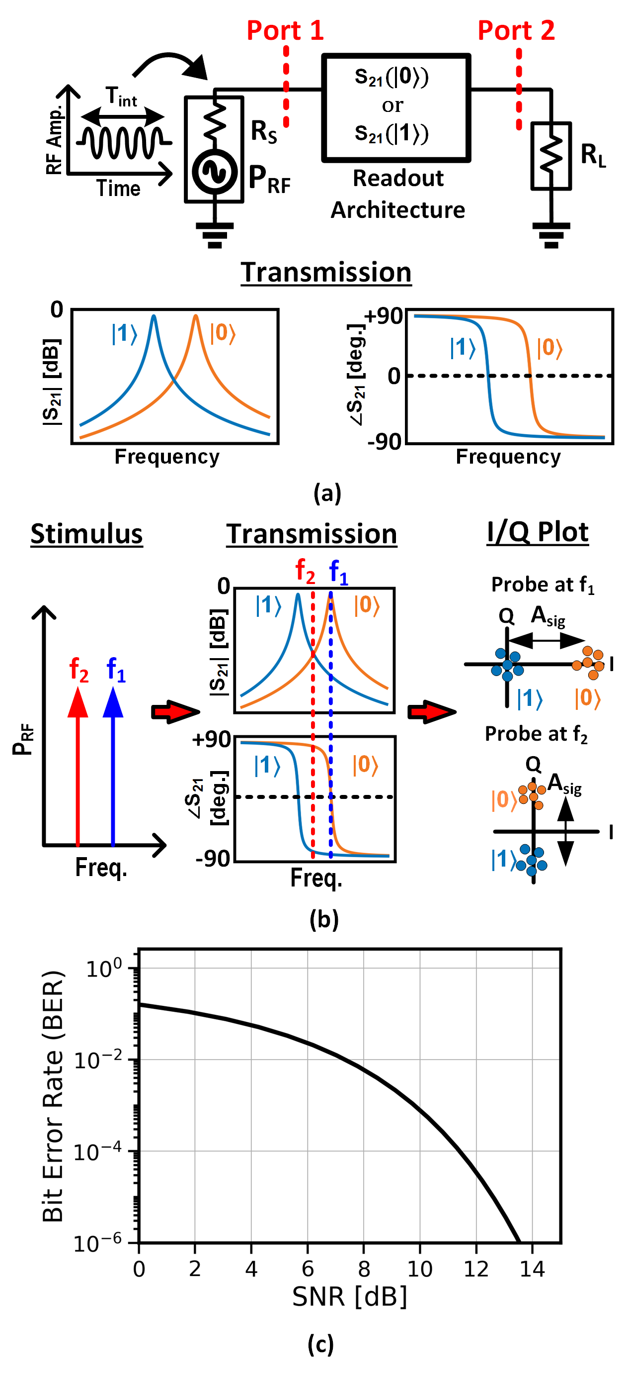
A simplified model of a gate-based readout architecture is illustrated in Fig. 1(a), where port-1 and port-2 indicate the input and output ports of the readout system, respectively. In principle, the readout architecture has a state-dependent transmission (or reflection) behavior dependent on the qubit’s state. To read the qubit’s state, the system is probed with a radio-frequency (RF) tone from port-1 with a certain time duration, . Depending on the frequency of the stimulus tone, the readout tone observed at port-2 exhibits a change in amplitude or phase, providing information about the qubit’s state. As an example, Fig. 1(b) illustrates the readout system’s response when probed at and . When the system is probed at the resonance frequency of the state (), the readout signal observed at port-2 resembles a binary amplitude shift keying signal (BASK), due to the attenuated response. On the other hand, when the system is probed at a frequency precisely between the or responses (), the output signal at port-2 resembles a binary phase shift keying signal (BPSK), where the and response differs by 180 degrees. Regardless of how the output signal is modulated, the readout signal can be denoted as in the constellation diagram, which describes the separation between the two states’ responses.
In general, the readout signal (i.e., ) must be large enough to accommodate the thermal noise contributed by the environment and the additional noise of the subsequent readout electronics, which is responsible for amplifying and down-converting the readout signal. To quantify the effect of the noise on the readout signal, the readout signal-to-noise ratio (SNR) must be calculated, which depends on both the power of the readout signal () and the total noise observed at the input of the readout electronics (). Mathematically, is related to by
| (1) |
where is the power delivered by the RF source to the input port of the system (i.e., port-1), is the readout angular frequency and is the state-separation factor, which depends on the behavior of the system when it is in the or state. The noise power, , on the other hand, can be expressed as , where is the noise power spectral density, which includes the noise of the electronics referred to port-2, and is the integration time. By defining the SNR as , the readout SNR can be expressed as
| (2) |
However, the quality of the readout acquisition is commonly characterized using metrics such as the bit error rate (BER) (equivalently, the readout infidelity, ) rather than the SNR. The relationship between the SNR in (2) with the BER can be described as
| (3) |
where is the tail distribution function of the standard normal distribution. Based on (3), the resulting BER for a given SNR performance is shown in Fig. 1(c). In fault-tolerant QC with QEC, a target BER of 10-4 is often desired, which corresponds to an SNR requirement of 11.5 dB.
The target SNR of 11.5 dB can be achieved in numerous ways, based on (2). Given a readout system with a certain state-separation factor, one could choose an arbitrary , , and a that complies with the desired SNR. However, in the context of QEC, is commonly fixed based on the QEC requirements. Thus, only and are left to be optimized to achieve the required SNR. By maximizing , can be made larger while still achieving the desired SNR. The larger tolerable benefits the readout electronics by allowing them to be designed at a lower power. With the limited power budget available at the cryogenic level of the dilution refrigerator, this approach enables better integration of cryogenic electronics suitable for future large-scale integration.
Experimental observations, however, have shown that increasing does not necessarily improve the readout SNR [9, 10, 11]. Theoretically, (2) shows a boundless trade-off between and , where a large allows to be increased proportionally for a given target SNR, , and state-separation factor, contradicting experimental observation. Thus, the limit in which can be relaxed as increases remains unclear. In this article, we investigate the validity of (2) by first constructing a qubit model that considers its quantum mechanical behavior during readout. The proposed model is used to simulate the behavior of a readout system to investigate the validity of (2) and the limitations of the trade-offs between and . To confirm the behavior shown by our proposed model, the simulated results are compared with experimental results.
The article is organized as follows. Section II first discusses the behavior of the qubits during readout and how they can be modeled. Section III presents the simulation results of the readout system when the proposed qubit model is considered. Section IV compares the simulated results with experimental results, verifying the validity and limitations of the model. Upon experimental verification, Section V discusses the impact of the trade-offs between and on the readout architecture. Section VI concludes the article.
II Spin Qubit Readout Theory
II.1 Double Quantum Dot
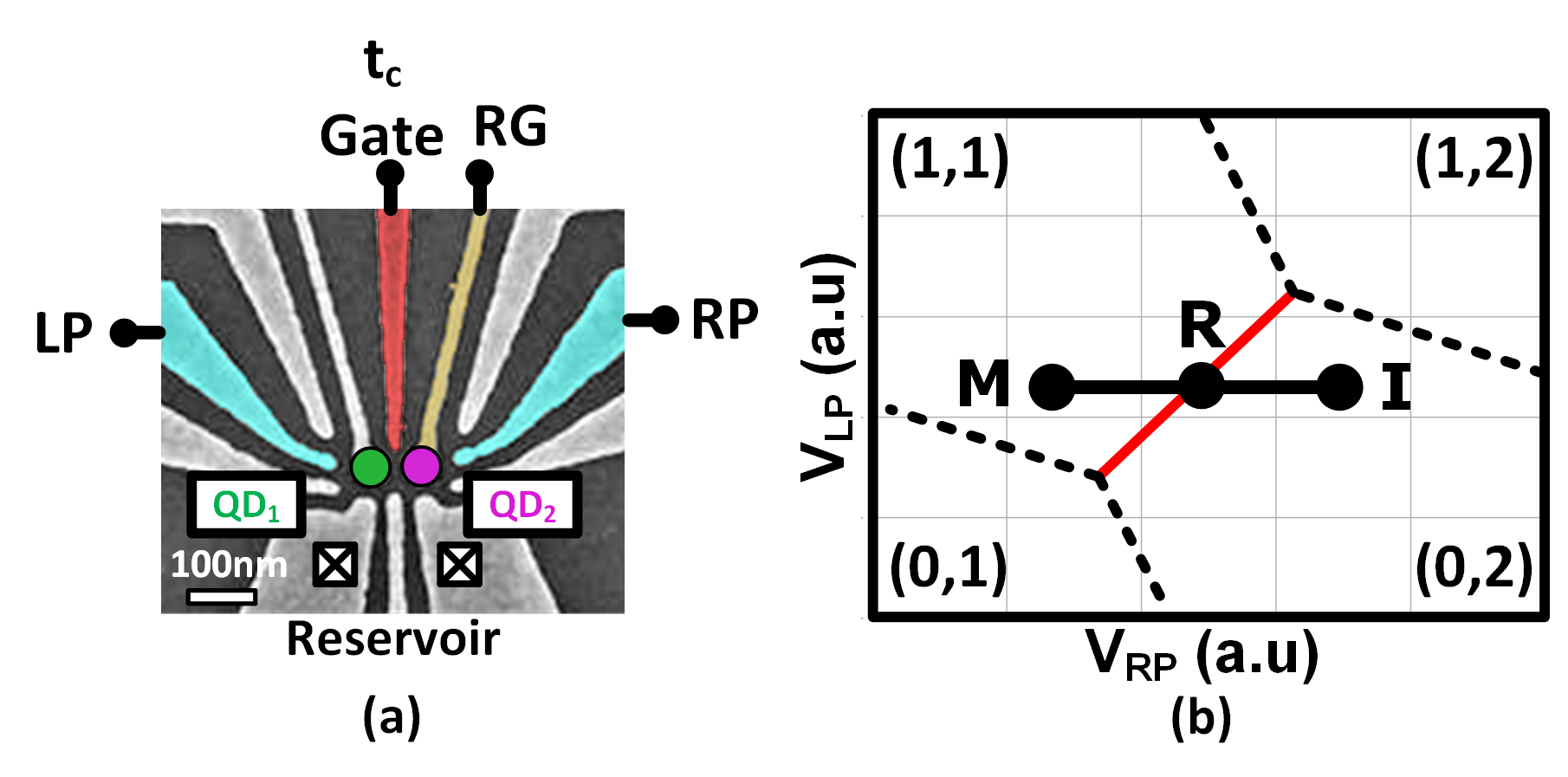
The double quantum dot (DQD) is the basic building block of a semiconductor spin qubit. Similar to a transistor, the DQD is composed of several plunger gates to control the potential landscape of the device to trap electrons in each respective quantum dot (QD), as indicated by the green and purple circles in Fig. 2(a). By varying the left () and right () plunger gate voltages, individual electrons can be loaded in and out of each QD site from the electron reservoir, as indicated by the crossed boxes in Fig. 2(a). The tunnel coupling () gate shown in the figure controls the tunnel coupling interaction between the two QDs and plays an essential role in tuning the device for readout.
The DQD is typically characterized by the charge stability diagram, as shown in Fig. 2(b). The number (NL,NR) indicates the number of electrons in the left and right QD, respectively. The dotted black lines in the diagram indicate the plunger gate voltages at which the electrons from the QD can be loaded or unloaded to the reservoir. For quantum computation with spin qubits, initialization can take place in the (0,2) regime, marked as ’I’ in Fig. 2(b). Once initialized, qubit manipulation can be executed in the (1,1) charge regime at point ’M’, where the electron spin in the left QD can be manipulated independently while keeping the right QD unaffected such that it can be used as a reference for readout [5]. To read the spin state of the left QD, the DQD is biased at the interdot regime (highlighted in red in Fig. 2(b)). Depending on the final spin state to which the DQD collapses, the electron may oscillate or stay in each respective dot in response to an RF tone applied at the readout gate (RG), leading to a state-dependent behavior, as discussed in detail below.
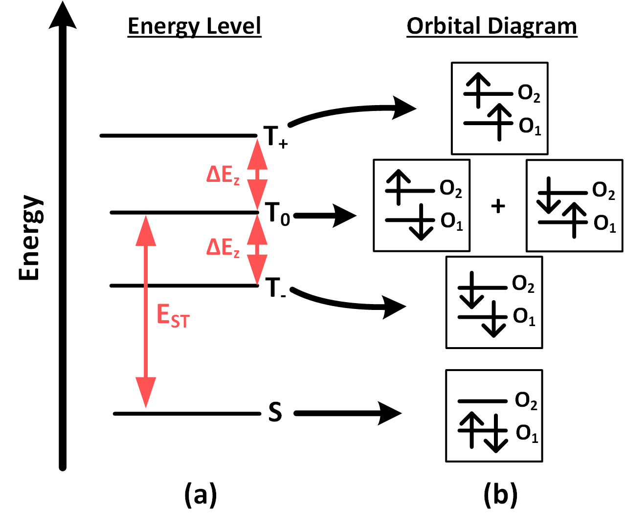
The spin states of the DQD and their energy levels in the (1,1)-(0,2) charge regimes must be evaluated to understand how the state-dependent behavior is manifested during readout. Generally, a two-electron system has four possible spin states when subjected to a magnetic field within a QD site. The four possible configurations are namely the singlet (S) and the three triplets (T-, T0, and T+) states, as illustrated in Fig. 3(a). The difference in energy between the T0 and the T- (T+) state is denoted as the Zeeman energy (Ez), while EST denotes the energy difference between the S and T0.
Fig. 3(b) depicts the corresponding orbital diagram for the two-electron system for the singlet and triplet states. Only the two lowest orbitals in which electrons can occupy are considered (i.e., O1 and O2). When the DQD is biased in the (0,2) charge regime, these orbitals are spatially confined to only the right QD site, while they spread out across the DQD when biased in the (1,1) charge regime. Due to the Pauli exclusion principle, each orbital can only be occupied by two electrons of opposite spins [12]. Consequently, only the singlet state can contain two electrons occupying the same orbital.
The energy levels of the singlet and triplet configurations for the (1,1) and (0,2) charge configurations are plotted together in Fig. 4(a). The sketch’s left and right columns indicate the singlet and triplet energy levels for the (1,1) and (0,2) charge configurations, respectively. The figure illustrates when the DQD is at the interdot regime, equivalently described as the zero detuning condition ( = 0). Here, the detuning parameter () is defined as the energy difference between the S(1,1) state and the S(0,2) state. In case the DQD collapses to a singlet state, an electron from one QD can freely tunnel to another at the zero detuning as the S(1,1) and the S(0,2) states have similar energy levels. In contrast, an electron cannot oscillate back and forth when the DQD is in a triplet state, as there are no overlapping triplet states when = 0.
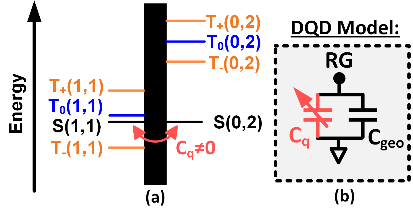
As the electron moves between the QD sites due to an RF readout signal applied at RG, quantum capacitance is generated [13]. Consequently, the DQD can be modeled as two parallel capacitors during readout, as illustrated in Fig. 4(b), where the capacitance contribution comes from namely the geometric capacitance () and the state-dependent quantum capacitance (). Thus, modeling the readout behavior of the system relies on quantifying the impact of quantum capacitance, which is the main focus of the subsequent section.
II.2 Quantum Capacitance Theory
As defined in [14], the quantum capacitance exhibited by the DQD is expressed as
| (4) |
where is the energy level of the singlet or triplet state of a DQD and is the lever arm of the DQD device, and is given by
| (5) |
where is the electron charge, is the capacitance of the readout gate, and is the total geometric capacitance of the DQD.
To calculate the quantum capacitance contribution from the singlet or triplet state expressed in (4), the energy level of the DQD for different detunings must be calculated in each respective configuration. This can be achieved by solving the DQD’s Hamiltonian using the Fermi-Hubbard model[15]. However, solving the total Fermi-Hubbard Hamiltonian of the DQD can be too complex and cumbersome. As we are only interested in the relevant features of the DQD under readout conditions, we simplify the DQD model and approximate the behavior by examining the Hamiltonian of a five-level system consisting of the ground and excited states of the S(1,1)-S(0,2) state and the three (1,1) triplet states. In general, the Hamiltonian for the S(1,1)-S(0,2) singlet state can be expressed by
| (6) |
where is the tunnel coupling, and are the Pauli matrices [16]. By solving the Hamiltonian with the time-independent Schrodinger equation, one can obtain the energy levels of the DQD for the singlet state as a function of detuning, expressed as
| (7) |
Furthermore, the energy levels of the (1,1) triplet state as a function of detuning can be approximated by [13]
| (8) | ||||
| (9) |
where is the electron gyromagnetic ratio, is the Bohr magneton constant, and is the applied magnetic field.
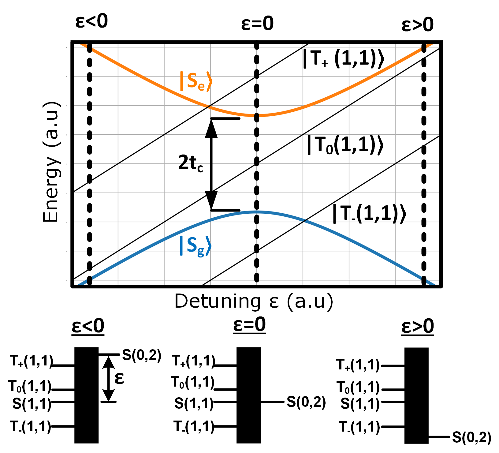
The energy levels of the singlet and triplet states expressed in (7)-(9) as a function of the detunings are plotted in Fig. 5. By plugging the energy expression (7)-(9) to (4), the induced quantum capacitance of the singlet and triplet states can be respectively derived as
| for , | (10) | ||||
| for , | (11) | ||||
| for and . | (12) |
Note that only the singlet state contributes an additional quantum capacitance during readout due to the curvature of the energy level. Moreover, the ground singlet state produces a positive quantum capacitance, whereas the excited singlet state produces a negative quantum capacitance. In contrast, no quantum capacitance contribution exists when the DQD is in the triplet states, as their energy levels are linearly dependent on .
As previously mentioned, the right QD can be used as a reference spin for readout, in which its spin is initialized to a spin down and is used to compare the spin state of the left QD. Consequently, the two lowest energy levels used as the computational basis are the and states [see Fig. 3]. For convenience, the two computational basis states used for the analysis are referred to as the and the state for the rest of the paper unless stated otherwise.
Based on the developed equations and theory for quantum capacitance, we can discuss and model the DQD behavior during readout in the following subsection.
II.3 Quantum Capacitance During Readout
In practice, the readout operation involves averaging the signal response of the system over many RF cycles to increase the SNR. Since the signal is averaged during readout acquisition, the quantum capacitance that the DQD contributes is also effectively averaged out. To illustrate this, based on (10), the quantum capacitance profile versus is illustrated in Fig. 6(a). Under the assumption that the readout gate (i.e., RG) is driven by a signal in the form of , the detuning value changes sinusoidally over each RF cycle:
| (13) |
in which, the role of the lever arm () is to convert voltage quantities to energy, with denoting the signal’s amplitude, and as the angular frequency of the applied signal. Consequently, as shown in Fig. 6(a), the value of the quantum capacitance varies along the shaded region due to the sinusoidal excitation. Due to the readout acquisition’s averaging nature, the quantum capacitance’s effective value seen during readout is the weighted average of the quantum capacitance value across the shaded region. By substituting (13) into (10), the effective quantum capacitance can be expressed as
| (14) |
Provided that the integration time is an integer multiple of the RF readout signal’s period (i.e., = ), a closed-form expression for can be obtained,
| (15) |
where, is an elliptical integral expressed as
| (16) |
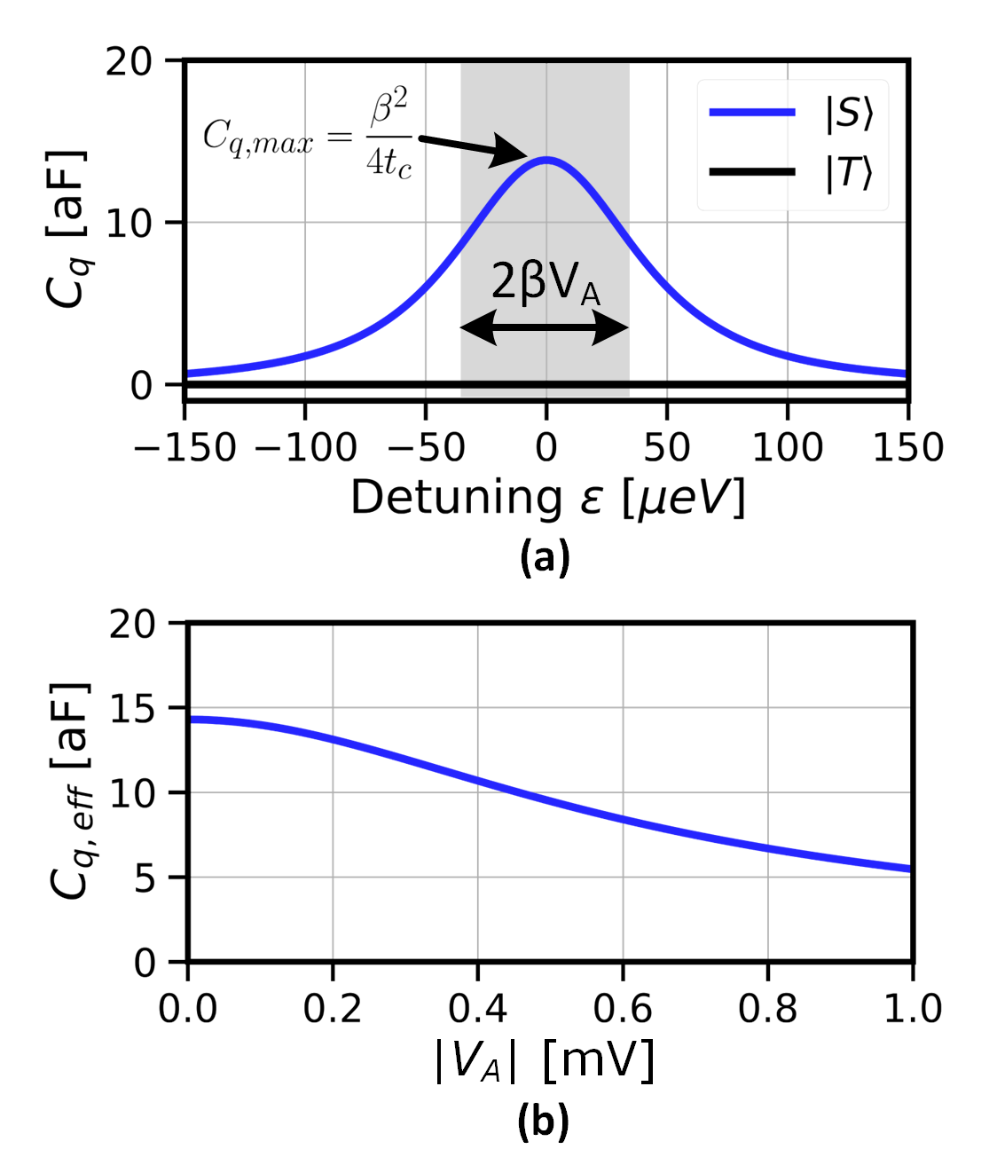
The effective capacitance for different readout amplitudes is plotted in Fig. 6(b), which is based on the result of (15). A smaller readout excitation is observed to induce a larger effective quantum capacitance due to the smaller averaging window, which only captures the peak of the quantum capacitance profile. At small readout voltages, converges to , in line with (10) when = 0. Also, note that a small readout excitation degrades the readout signal [see eq. (2)], which may reduce the SNR for a given fixed . Hence, a longer may be required to regain the same SNR. In contrast, a larger readout excitation implies a smaller effective quantum capacitance, which may, in effect, decrease the frequency shift of the response between the and states. This behavior is reflected in the state-separation factor between the and and consequently may lower the SNR as described in (2).
II.4 Optimum Tunnel Coupling
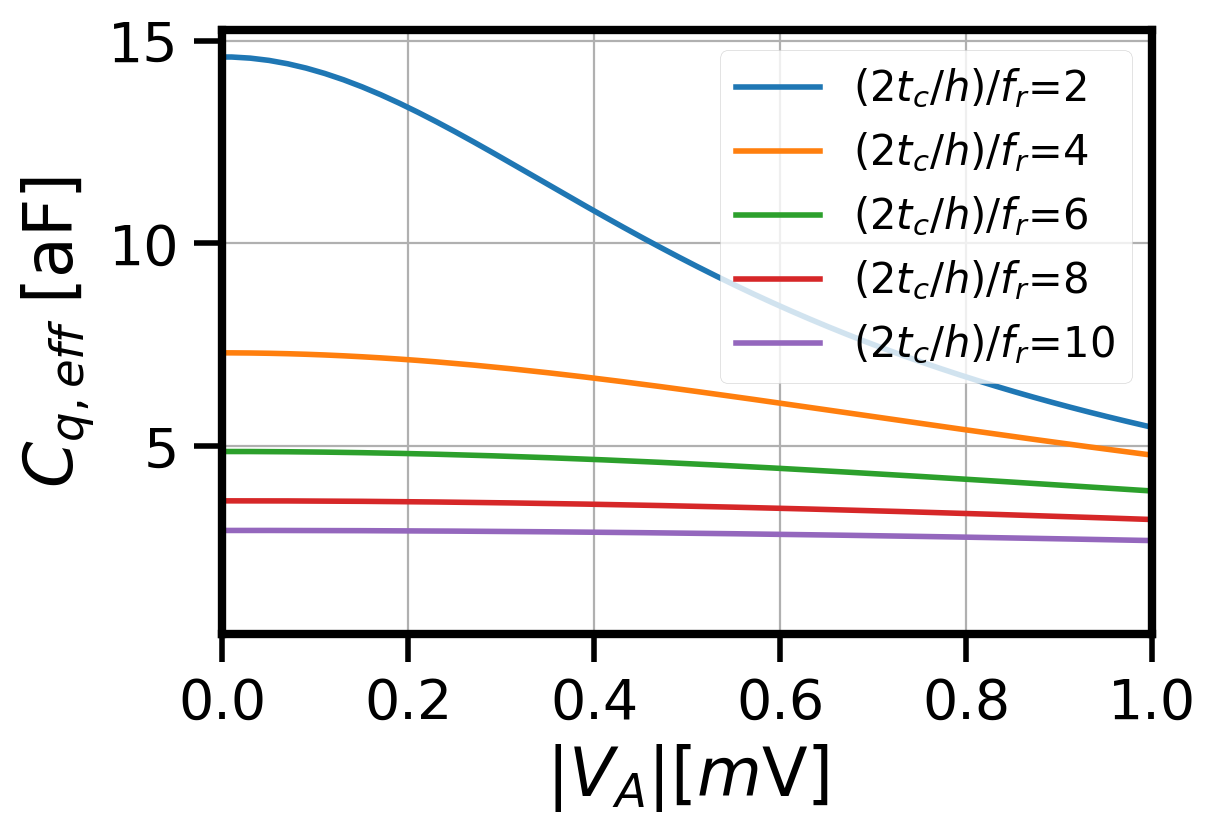
It should be noted that the tunnel coupling can significantly influence the behavior of the qubit during readout. When the tunnel coupling is set too low, the energy gap between the band and the band diminishes [see Fig. 5]. As the band gets closer to the state, the system can transition between the and energy bands instead of staying in the band, which is necessary for the system to realize quantum capacitance. For the assumption presented here to be valid, the system must be biased in the adiabatic limit, bounded by [13], where is the readout frequency and is the Planck constant. The system is more adiabatic and less likely to transition between the and state as the ratio between the tunnel coupling and the readout frequency increases.
The for different adiabaticity factors are plotted in Fig. 7. While it is desired to operate below the adiabatic limit, it is observed that larger quantum capacitance is observed by biasing the DQD closer to the limit, which can increase the sensitivity of readout. Based on the observation, the qubit must be biased close to the adiabatic limit (i.e., ) to maximize the quantum capacitance contribution.
II.5 Lever Arm
The quantum capacitance can also be increased by means of the lever arm () to increase the readout sensitivity, as described by (10). The lever arm can be increased by designing the QD devices with quantum wells closer to the gate electrodes or by implementing the device in a silicon substrate, similar to a CMOS process [17, 18]. While the approach aligns well with the future goal of monolithic integration with CMOS electronics, these devices tend to have faster decoherence times as the qubit is located closer to the gate dielectric interface [18]. Thus, increasing the lever arm will need careful consideration as it influences multiple factors other than the readout performance.
III Readout Simulation
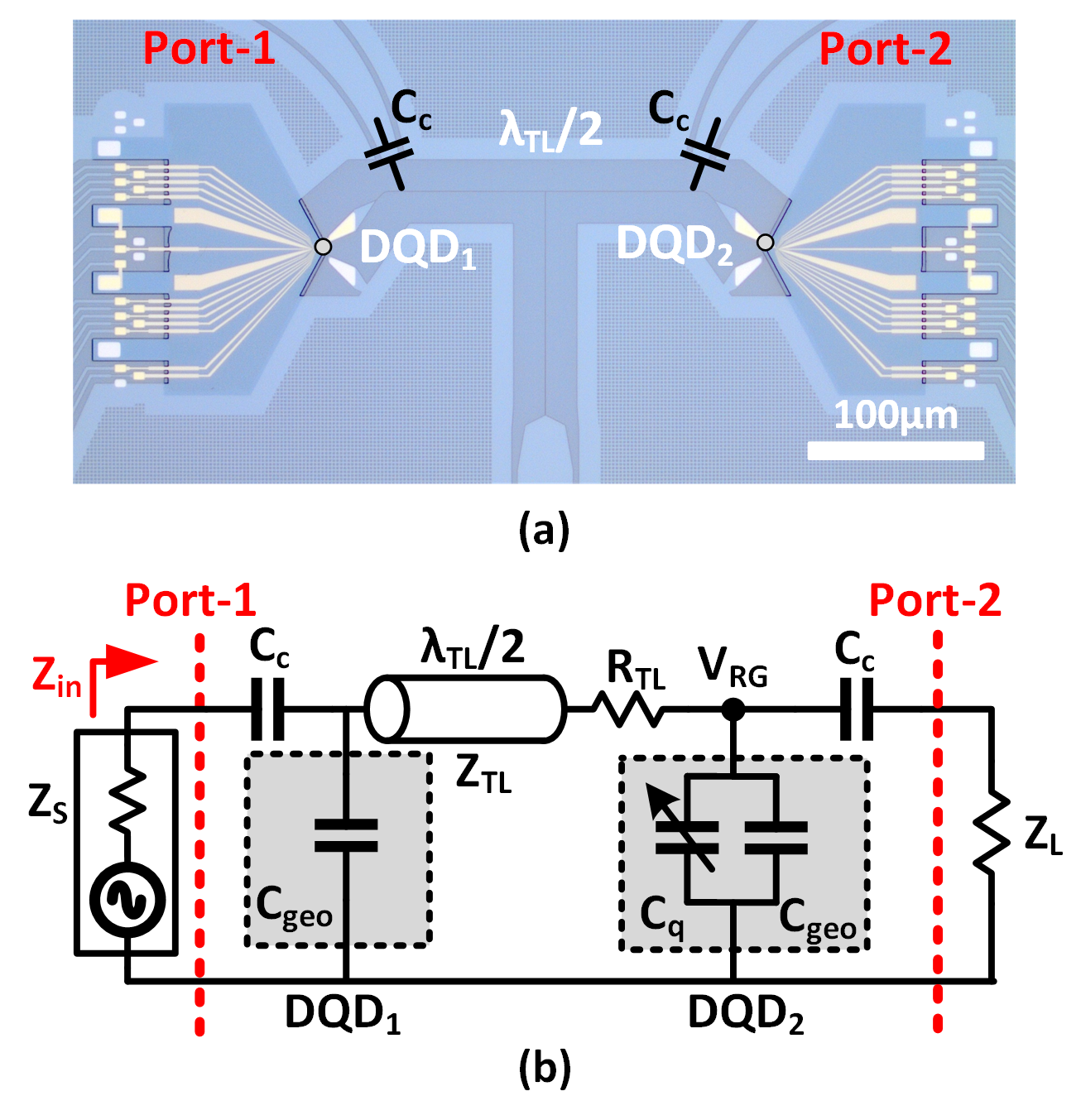
The quantum capacitance model introduced in the previous section can now be applied to a qubit sample that has been measured previously [19]. The qubit micrograph is shown in Fig. 8(a). The sample, realized in 28Si/SiGe heterostructure, consists of 2 DQD sites separated by a 250m half-wavelength superconducting transmission line fabricated with NbTiN material. The half-wavelength transmission line is AC coupled to the input and output ports (port-1 and port-2) through the coupling capacitors . The DQD2 is biased at the zero detuning regime, thus exhibiting a geometric and quantum capacitance during readout when DQD2 is at the state. Moreover, the DQD1 is tuned in the (0,0) charge regime and thus only contains a fixed geometric capacitance. The sample is probed with an RF signal from port-1. The RF tone’s corresponding phase or amplitude change can be detected by measuring its in-phase (I) and quadrature (Q) signal components at port-2 using an I/Q RX.
The complete electrical model of the sample is shown in Fig. 8(b). To model the state-dependent capacitance of DQD2, a voltage-dependent capacitor is included in the circuit, and its value depends on the voltage at the readout gate [see Fig. 2]. A resistor (i.e., ) is also included in series to the transmission line in the schematic to model the system’s loss, which can originate from resistive and dielectric losses in the sample [20]. When comparing the simulation with the measurement results, is used as a fitting parameter based on the measured resonator’s bandwidth. In the simulation, the quantum capacitance contribution is realized by a lookup table (LUT) VerilogA model, relating different readout gate voltage levels to distinct values using (10) and DQD properties summarized in Tab. 1.
| Quantity, Symbol | Value |
|---|---|
| Tunnel coupling, 2/h | 14.1 GHz |
| Lever arm, | 102 meV/V |
| Characteristic resonator impedance, | 4.5 k |
| Characteristic impedance of system, | 50 |
| Geometric DQD capacitance, | 1.9 fF |
| Coupling capacitance, | 0.32 fF |
| Series resistance, | 17 |
III.1 Frequency Shift
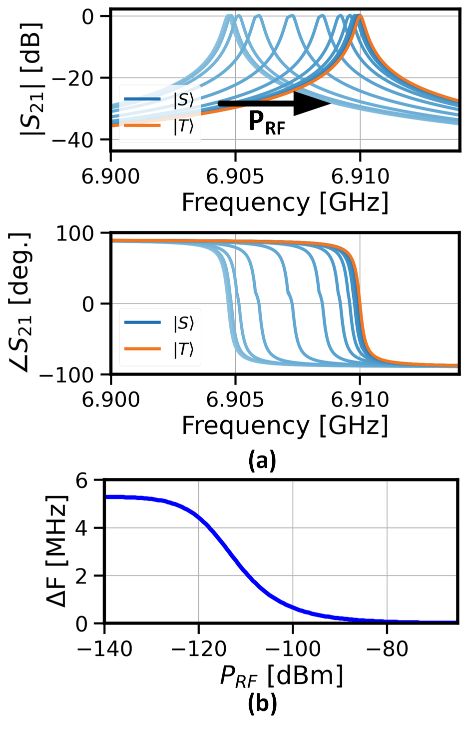
The transmission (S21) behavior between port-1 and port-2 for different values is plotted in Fig. 9(a). The orange and blue lines in the plot indicate the transmission response when the DQD is in the and the state, respectively.
To gain more insight into the (S21) behavior, it is instructive to see the behavior of the input impedance of the sample. For simplicity, a large coupling capacitor and a lossless system are first considered such that the input impedance of the sample can be approximated as
| (17) |
where is the physical length of the transmission line, and is the load impedance (equal to 50 ). is the effective characteristic impedance of the transmission line defined as , where is the inductance per unit length and is the effective capacitance per unit length of the transmission line, including the capacitance of the DQD. Additionally, is the phase constant defined as
| (18) |
where is the angular frequency where the expression is evaluated. On resonance, (17) simplifies to 50 as approaches 0. In effect, all the power provided by the source () is delivered to port-1 and consequently also delivered to the load at port-2, resulting in a 0 dB response in the plot [see Fig. 9(a)]. Away from resonance, tends to be large, thus approaches . Due to the system’s large , reflection at the input plane occurs, leading to an incomplete power transfer to . This reflection contributes to the observed bandpass response in the plot.
The resonant condition requires that the term in (17) be equivalent to , such that simplifies to 50 . Consequently, the resonant frequency can be derived based on (18) and can be recast as
| (19) |
where and are the transmission line’s total equivalent lumped inductance and capacitance, respectively. Note that , has two different loading conditions depending on the state of the DQD2, which can be described as
| (20) |
where is the equivalent lumped capacitance of only the bare transmission line, excluding the DQD’s contribution.
When DQD2 is in the state, is only affected by . On the other hand, when DQD2 is at the state, is affected by and , which leads to a lower , as observed from Fig. 9(a). Additionally, when the system is subjected to a strong RF readout signal, is averaged over a larger span. This results in a lower , causing a smaller resonant frequency separation between the and the response.
To further increase the separation of the resonant frequency between the and state, it is necessary to increase the capacitance ratio. Hence, must be maximized while keeping and low. A higher can be achieved by increasing the lever arm of the device with the drawbacks mentioned in Section II. On the other hand, can be kept low by designing the transmission line with a large characteristic impedance.
The simulated resonant frequency shift difference (i.e., ) of the -state relative to the -state for different input probe power is summarized in Fig. 9(b). At low readout power, a 5 MHz frequency shift is seen. However, the frequency shift becomes smaller at higher probe power as approaches , which aligns with the presented theory.
III.2 Readout Signal and Probe Frequency
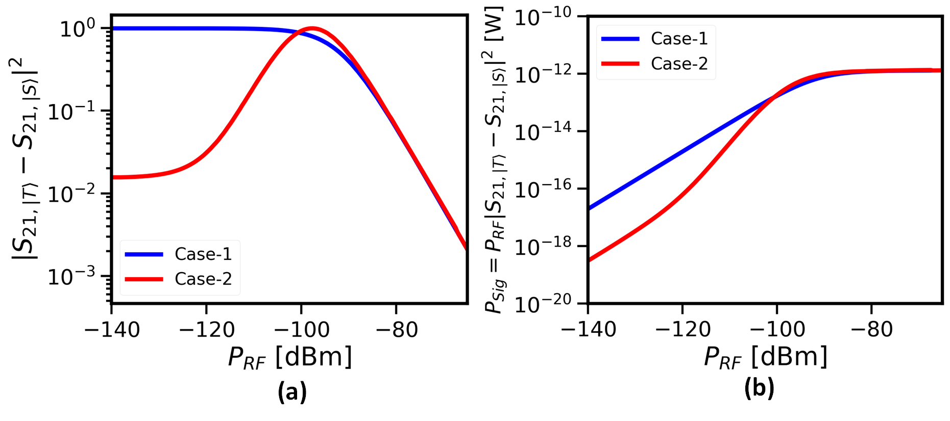
To determine the readout SNR, the readout signal’s power at port-2 must be calculated. However, the behavior of the readout signal depends on the frequency at which the system is probed. This section explores the behavior of the readout signal in two scenarios: (1) when the system is probed at the resonant frequency of state (i.e., 6.91 GHz) leading to a BASK response, and (2) at the frequency halfway in between the resonant frequency response of the and state, leading to a BPSK response.
As expressed in (1), the readout signal’s power () is defined as the product of the state-separation factor and the power applied to the readout sample. The simulated state-separation factor (i.e., - ) for both cases are plotted in Fig. 10(a). In case-1, the state-separation factor is shown to be approximately 1 for low readout probe power. In this condition, the term is significantly smaller than the term when probed at the resonance of the state. Consequently, the response is attenuated during readout compared to the response, resembling a BASK readout signal, as discussed previously. In case-2, the state-separation factor is shown to be smaller than case-1 at low readout power. In this condition, both the and terms are generally small when probed between the and resonant frequencies. This results in a readout response that is both attenuated and exhibits a 180-degree phase difference between the and readout response, akin to a BPSK signal. Interestingly, as the applied input power increases, the state-separation factor converges, reflecting that the resonant frequencies of the and states converge.
The readout signal’s power is shown in Fig. 10(b). Remarkably, the plot shows a saturation in the readout signal power due to the decrease in the state-separation factor with the application of higher readout probe power. As the readout signal power dictates the readout SNR [see eq. (2)], the simulation implies that there is a maximum achievable SNR for a given qubit property. Interestingly, in a different way and based on the time-dependent charge population in the DQD under RF excitation, [21] also theoretically predicted the saturation in the readout signal. However, the work in [21] did not consider the power-dependent frequency shift and did not present any experimental results to support the theory.
From this observation, performing a readout shown by case-1 is generally recommended, as it yields a larger readout signal response even at lower probe power, leading to a higher SNR even at lower probe power. Furthermore, from a practical point of view, readout at the bare resonant peak of the resonator is simpler as the readout frequency is fixed and does not need to be changed to account for the power-dependent resonant shift. Based on this reasoning, the experiments in this paper follow the readout behavior shown by case-1.
III.3 Noise Estimation
The power spectral density of the system’s noise () at the input of the readout chain can be expressed as ( W/Hz), where is the Boltzmann constant, and is the effective noise temperature of the readout system. Considering an ambient temperature of for the DQD sample, may be estimated by
| (21) |
where , , and are the noise temperatures of the traveling wave parametric amplifier (TWPA), low noise amplifier (LNA), and the RX, respectively, while and are the gain of the TPWA and LNA, respectively. Considering a TWPA gain of 28 dB (), the readout system’s noise performance is mainly dictated by the TWPA. Assuming that the TWPA is quantum-limited, its noise temperature can be approximated by = [22]. For an of 6.91 GHz, and a of 20 mK, the total noise temperature of the readout architecture () is estimated to be 350 mK.
III.4 Normalized Signal-to-Noise Ratio
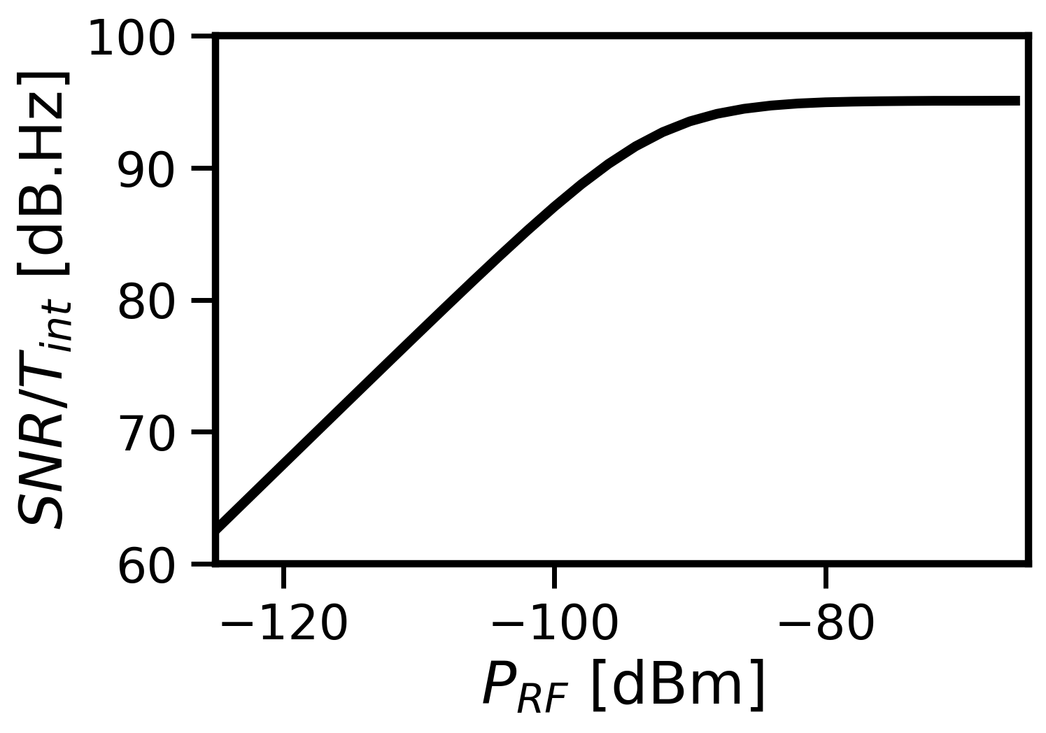
The behavior of the readout SNR can now be discussed. However, to properly evaluate the trade-off between and , it is far more instructive to define the normalized SNR: SNRN = = SNR/. In this way, we can compare the performance of the readout scheme independent of the chosen . The simulated SNRN, when assuming a of 350 mK and considering all the system parameters in Tab. 1, is plotted in Fig. 11. The SNRN firstly increases linearly with the probe power but finally saturates at a maximum of 95 dBHz. Considering a of 1 s, and assuming a quantum-limited readout chain, a theoretical maximum SNR of 35 dB is achievable.
With the theoretical framework for gate-based RF readout established, the measurement verification of the proposed model can now be carried out.
IV Measurements
IV.1 Measurement Setup
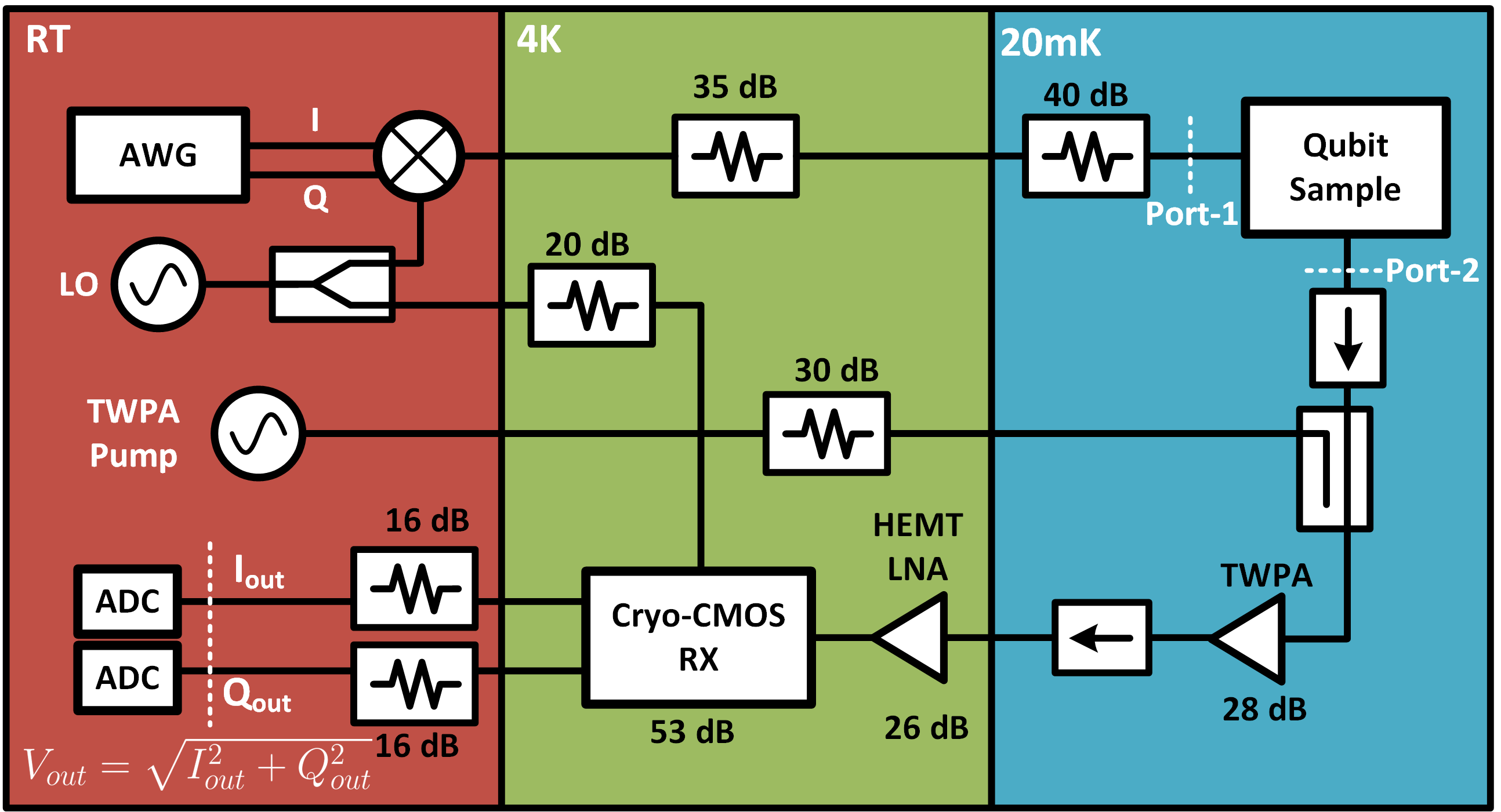
The complete measurement setup is shown in Fig. 12, similar to the ones used in [23, 19, 20]. The sample is mounted at the mixing chamber plate and cooled down to an ambient temperature of 20 mK. Alongside the qubit sample, a TWPA with 28 dB gain is installed to minimize the noise of the readout chain, thus allowing one to measure a low-power readout signal at various . The TWPA pump is generated at room temperature (RT) and fed to the TWPA by a coupler at the mixing chamber plate. An isolator is used between the qubit sample and the coupler to isolate the qubit from reflections due to the large TWPA pump tone. At the 4 K plate, a high electron mobility transistor (HEMT) LNA with a 26 dB of gain is used to amplify the readout signal further. An additional CMOS RX chip is mounted on this plate for signal downconversion and amplification [23]. At RT, two off-the-shelf 1 GS/s 8-bit ADCs are used to quantize both the I/Q signals, allowing for further digital signal processing at the baseband. A single LO source at RT is also used to drive the two mixers that upconvert and downconvert the readout signal to ensure phase synchronization. Moreover, a 75 dB attenuation in the input RF line is intentionally employed to ensure a proper thermal noise level at the input of the sample at the mixing chamber plate.
IV.2 Charge Stability Diagram
The stability diagram of the sample is measured and shown in Fig. 13(a). The diagram is obtained when the qubit sample is read out at the bare resonance frequency (i.e., 6.91 GHz) for different and values. A clear distinction between different charge states can be observed, especially at lower charge population regimes.
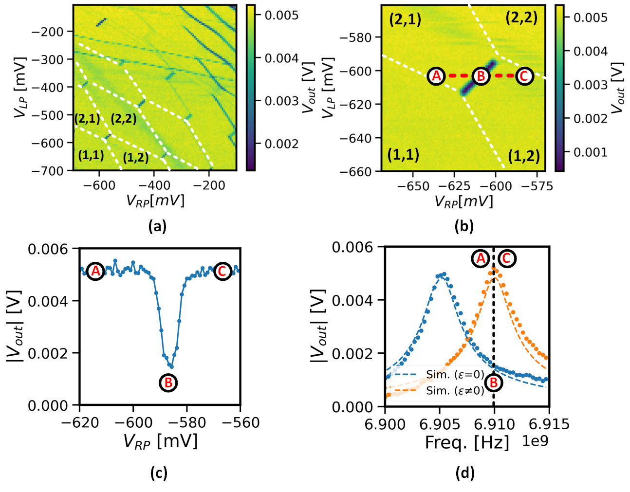
The behavior of is verified in the (2,1)-(1,2) charge state. Considering that the quantum capacitance is generated by forcing an electron to oscillate across the DQD site under RF excitation, the behavior in the (2,1)-(1,2) regime is similar to the (1,1)-(0,2) regime discussed previously since the experiment isolates only the quantum capacitance contribution behavior. The charge stability scan around the (2,1)-(1,2) charge state is shown in Fig. 13(b). To understand the effect of the quantum capacitance during readout, a line cut is taken across the interdot crossing, and its corresponding result is depicted in Fig. 13(c). At point (A), the DQD is not loaded by the quantum capacitance as it is far from the zero detuning ( = -620 mV). As shown previously, averaging the quantum capacitance well away from the zero detuning results in a net zero effective quantum capacitance, which emulates the behavior of the state. In contrast, point (B) is located where the system is at zero-detuning ( = -590 mV), where the maximum quantum capacitance contribution can be observed. Due to the quantum capacitance contribution, the resonator’s resonance frequency shifts to a lower frequency, which, in effect, lowers the observed output voltage. As more positive is applied to the DQD ( = -560 mV), the system returns to the response observed at (A).
The shift in the resonance frequency of the resonator can also be observed in Fig. 13(d). The data is obtained by monitoring the magnitude of the downconverted I/Q voltages (i.e., ) when the frequency of the probe signal is swept from 6.9 GHz to 6.915 GHz. For comparison, the simulation results are also included in Fig. 13(d) using the dotted lines, which show a good agreement with the measurements. The orange line in the figure depicts the response when the system is away from zero detuning ( = -620 mV), while the blue line depicts the system’s response at zero detuning ( = -590 mV). The mapping of points (A), (B), and (C) from Fig. 13(c) are also labeled in Fig. 13(d) for clarity. As predicted from the simulation, a 5 MHz frequency shift is observed for the zero-detuning response at very low power.
IV.3 Frequency Shift
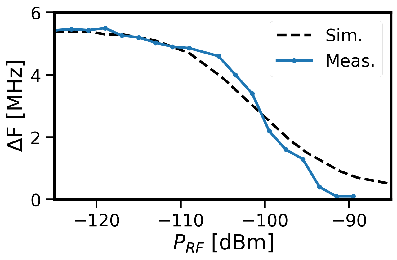
Given that the quantum capacitance cannot be measured directly, we can only observe the manifestation of the quantum capacitance through the frequency shift response of the sample. To verify this, the frequency at which the maximum transmission is observed is tracked at zero detuning and non-zero detuning conditions while sweeping the probe tone power from -125 dBm to -89 dBm, referred to the port-1 plane in Fig. 12(c). The frequency difference () is defined as the difference between the resonance peaks of the non-zero and zero detuning responses. As shown in Fig. 14, the frequency shift of the DQD decreases for higher input power, following the trajectory dictated by the developed theory and simulation results. Interestingly, the frequency shift reaches 0 faster than in the simulation. This behavior is discussed in the following section.
IV.4 Readout Signal
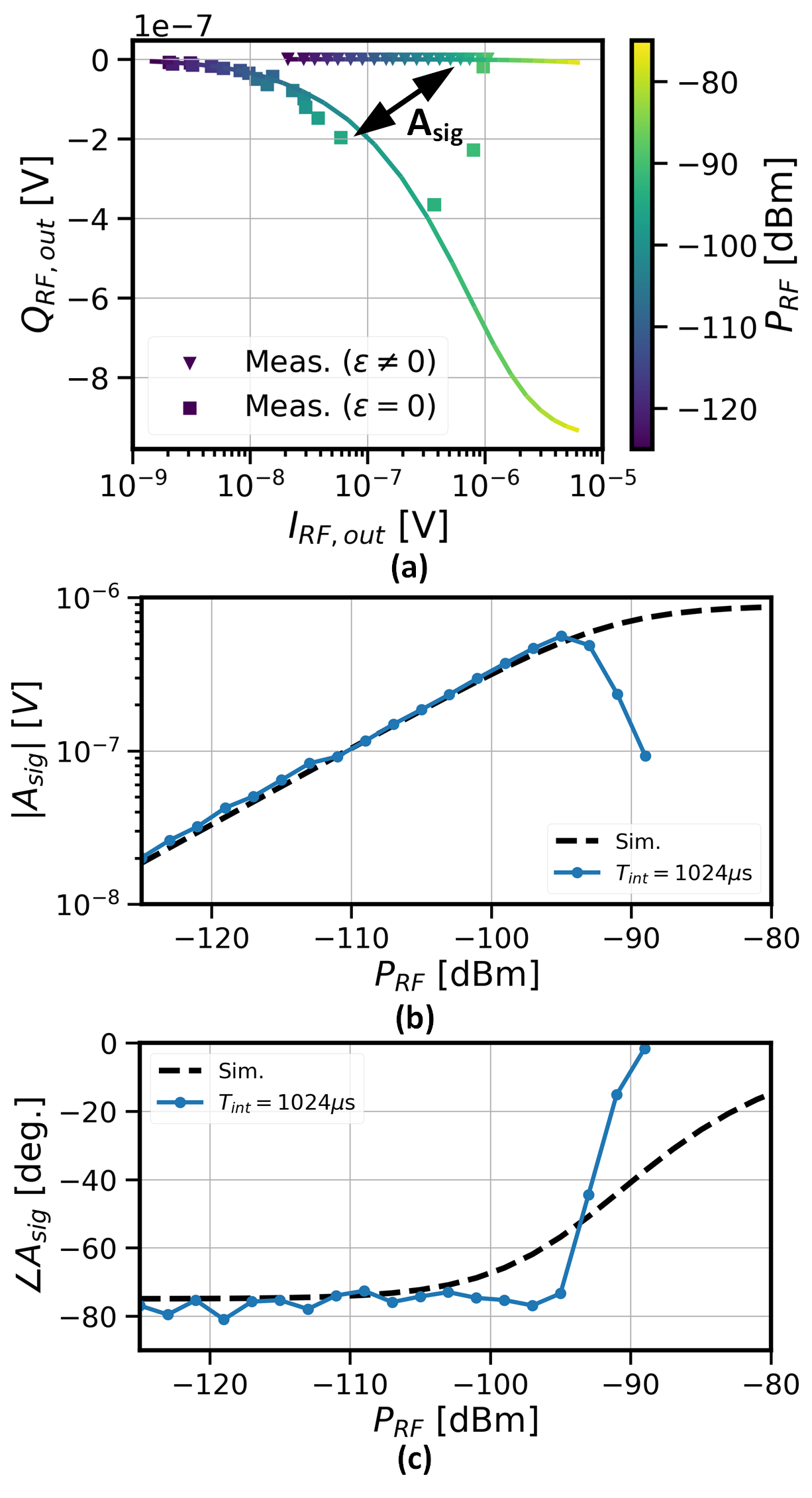
The simulated and measured readout I/Q responses for zero and non-zero detunings are illustrated in Fig. 15(a). The data is obtained by referring the measured I/Q data sets to the port-2 plane when the system is probed at the readout frequency of = 6.91 GHz. The triangle and square points indicate the non-zero and zero detuning responses, respectively. Note that the solid line indicates the simulated I/Q voltages, and the measured data points are color-graded based on the readout power applied to the sample. Based on Fig. 15(a), the I/Q points resemble an amplitude-modulated signal at lower readout power, where the zero-detuning response is close to the origin of the I/Q plane due to the attenuation of the shifted resonator response. At higher readout power, the zero-detuning I/Q response acquires an extra phase component as the resonant frequency of the zero-detuning response gets closer to the bare-resonance frequency of 6.91 GHz. The distance between the two responses is also reduced for the higher power, implying a decreased readout signal amplitude at a larger probe power.
As explained in Section I and shown in Fig. 15(a), the readout signal () is the distance between the qubit’s responses in the constellation diagram. The magnitude and phase of are respectively shown in Fig. 15(b) and Fig. 15(c). The simulated and measured and are seen to be in good agreement up to of -100 dBm. Beyond this point, a noticeable difference between simulation and measurement is observed, especially the measured . Compared to the simulation, at large probe power, the measured approaches 0 degrees faster, and the measured does not saturate but reduces significantly. Both magnitude and phase behaviors imply that the resonant frequency of the zero detuning response becomes the same as the bare resonance frequency of the resonator, consistent with the qualitative trend observed for in Fig. 14.
The discrepancy between the simulation and the measurement results at higher probe power levels can be attributed to several factors. The primary factor contributing to the reduced readout signal amplitude at large probe power levels is suspected to be associated with Landau-Zener transitions [24]. At a very large excitation, the rate at which the system’s detuning evolves with time (i.e., ) is fast enough such that the evolution is no longer adiabatic. Hence, the system can not be examined with a time-independent Hamiltonian, as initially assumed. In this regime, the system can undergo transitions between the and energy bands, as illustrated in Fig. 5, leading to a reduced readout response. Interestingly, this observation is consistent with the numerical simulation shown in [21], which predicts that the quantum capacitance contribution can be reduced to 0 when the system is assumed to be non-adiabatic. In addition to the Landau-Zener transitions, the reduction in the readout amplitude may also be caused by the resonator’s self-heating, which can cause the resonator’s quality factor to degrade at a very large excitation.
IV.5 Readout Noise
The standard deviation of can be used to estimate experimentally. By measuring the standard deviation of at the non-zero detuning regime between a of -570 mV to -560 mV (i.e., Point C in Fig. 13(c)), the integrated noise voltage can be calculated. Mathematically, this is equivalent to (V). Experimentally, is estimated to be 460 mK when referring to the input of the readout chain.
The measured is close to what was previously observed for a readout chain incorporating TWPA amplifiers [25, 26, 27]. However, it is 1.3 higher than the previous theoretical estimation (i.e., 350 mK). The discrepancy between the theoretical and measured values may stem from different contributions. First, is estimated by always assuming that is 20 mK, which may be higher in reality as reflected by the electron temperature. Moreover, the estimation did not account for the losses of the isolator and coupler in front of the TWPA.
IV.6 Normalized Signal-to-Noise Ratio
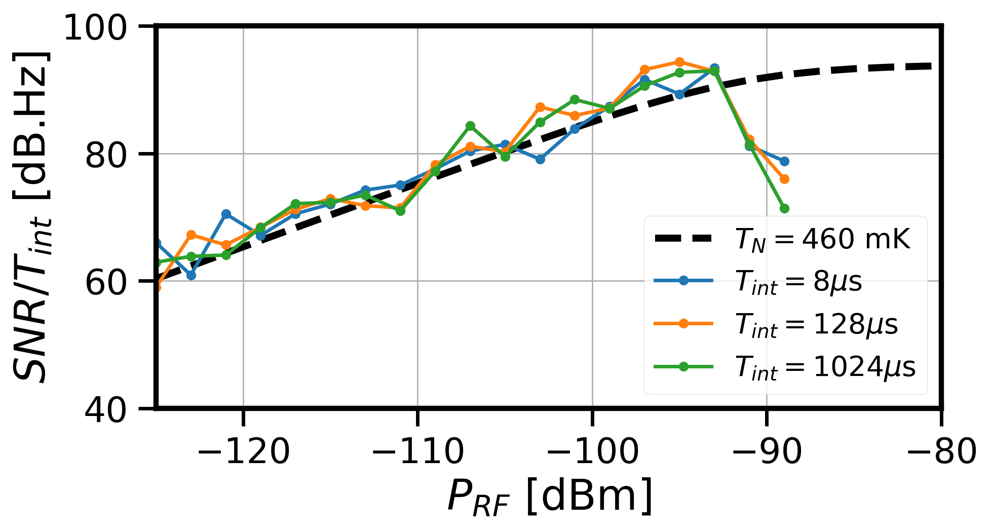
Fig. 16 shows the measured and simulated SNRN. The black dotted line indicates the simulated SNRN based on the previously simulated readout signal, with a of 460 mK. As expected, the data shows that the measured SNRN overlaps each other for different experiments. A maximum measured SNRN of 89 dBHz is observed at = -95 dBm, and SNRN degrades beyond this power level.
V Discussion
The previous section showed that the qubits’ resonant frequency shift is power-dependent. This section explores the implications of the power-dependent readout behavior, examines the associated trade-offs, and addresses the noise requirements for the readout chain.
V.1 Frequency Multiplexing Consideration
The measurement and model indicate that the readout power can control the qubit’s frequency shift. Thus, a higher readout power leads to the possibility of reading out more qubits per given bandwidth, resulting in a higher spectrum efficiency as the frequency spacing requirement between each qubit decreases. As depicted in Fig. 14, the frequency shift is estimated to be on the order of 2 MHz at the peak of the SNRN with a of -95 dBm. Assuming each qubit has a frequency shift of 2 MHz with a 3 MHz resonator bandwidth, each qubit has a channel bandwidth of 5 MHz. However, it should be noted the frequency spacing between the qubits cannot be too small as the readout pulse power, depending on the desired integration times, may leak into neighboring qubits, which eventually may require pulse shaping for a dense FDMA readout architecture.
It is important to note that the number of qubits that can be read out within a specific frequency range can be increased by narrowing the resonator bandwidth through a resonator design with a large characteristic impedance. However, there are practical constraints on how much the resonator bandwidth can be reduced. At very small resonator bandwidth, readout is mostly limited by the ring-up time of the resonator when given an RF impulse. Consequently, the readout response may not settle fully for a given , thus reducing the readout signal and, eventually, the SNR.
V.2 Optimum Tunnel Coupling and Readout Operating Frequency
Based on the discussion above, one could also ask about the preferable readout frequency for gate-based readout. Given a readout frequency , one must bias the such that = 2. Consequently, the tunnel coupling should be proportionally increased when the qubit is read at a higher to keep the system at the adiabatic limit. A lower frequency shift is expected when the qubit is read out at higher due to the lower quantum capacitance at higher bias. In addition, a higher readout frequency increases the power consumption of the electronics significantly, which can also limit the scalability of the readout system due to the limited power budget in the dilution refrigerator. However, operating at a higher readout frequency may decrease the footprint of the resonator, which can be beneficial when the system is scaled up.
The opposite behavior is expected when the readout frequency is lowered. Lower readout frequency implies a lower . Hence, a larger quantum capacitance is to be expected, which can increase the SNR. As the frequency of operation is lowered, power consumption of the electronics is also expected to follow suit. However, the larger quantum capacitance means that each qubit occupies a larger channel and limits the number of qubits occupying a certain bandwidth. Additionally, pushing the readout frequency lower leads to a larger area required for the resonator and may limit scalability.
V.3 Noise Temperature Requirement for Readout Electronics
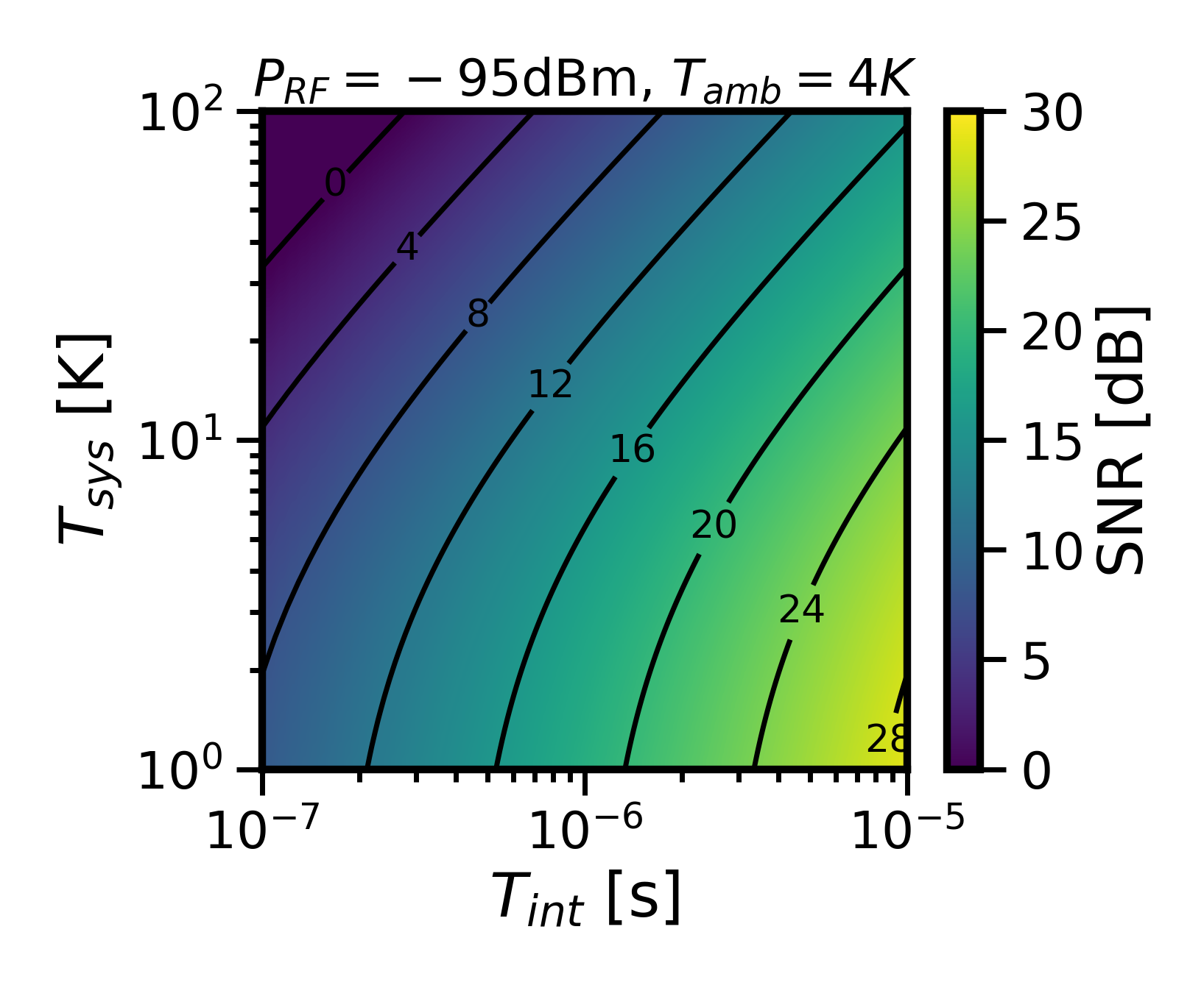
As discussed in Section I, an SNR larger than 11.5 dB is needed to achieve BER 10-4. Assuming a of 1 s, the maximum inherent SNR of the measured gate-based readout is 29 dB, extrapolated from SNRN of 89 dBHz [see Fig. 16]. Hence, an excess SNR of 17.5 dB allows one to increase by 56 and still satisfy the BER specification, resulting in a maximum of 25.8 K for the readout chain. Furthermore, assuming the readout electronics are now operating at 4 K, the readout chain should exhibit an input-referred noise temperature () of 21.8 K to still comply with a readout SNR of 11.5 dB — a significantly more relaxed noise requirement in comparison to the performance offered by TWPA and the HEMT LNA.
Fig. 17 shows the SNR for different and values when the system is probed at its maximum achievable ( = -95 dBm) while considering a of 4 K. Assuming a modest of 50 K based on the recently published cryo-CMOS RX design [23, 28, 29, 30, 31], the contour plot reveals that the prior-art cryo-CMOS receivers cannot satisfy the 11.5 dB target SNR at a of 1 s. As it is suspected that the noise performance of the cryo-CMOS receivers is limited by the shot noise [32] and the self-heating effect [33], passive amplification techniques should be investigated in the future to avoid large biasing currents required for active devices in LNAs [34, 35].
VI Conclusion
This work presents a theoretical framework that allows one to investigate the impact of the receiver’s noise temperature, readout probe power, and integration time on the SNR and fidelity of RF gate-based readout systems. Considering the qubit’s quantum mechanical behavior, a semi-classical model was developed that estimates the state- and power-dependent resonance frequency shift and intrinsic readout SNR. Following the trajectory dictated by the developed theory and simulation, the experimental results showed that the frequency spacing between the resonance peaks corresponding to different qubit states was reduced by increasing the power of the readout tone. This affects the separation between the qubit states in the constellation diagram and eventually limits the maximum achievable SNR of the gate-based readout systems. Moreover, based on the outcome of this study, different trade-offs among the qubit biasing, the readout SNR, the system’s footprint, the receiver’s operating frequency, bandwidth, and noise are discussed. Consequently, the presented guideline can help designers realize a scalable and low-power readout chain while obtaining a readout fidelity sufficient for fault-tolerant quantum computation.
Acknowledgment
This research was funded by Intel Corporation. The authors would like to thank G. Zheng and P. Harvey-Collard for fabricating the device, Z. Y. Chang, J. Mensingh, O. Benningshof, N. Alberts, R. Schouten, R. Vermeulen from TU Delft for measurement support, L. DiCarlo and his team for access to the 3He cryogenic measurement setup, L. P. Kouwenhoven and his team for access to the NbTiN film deposition, W. Oliver for providing the TPWA, and the members of the Spin Qubit team, the Cryo-CMOS team, M. F. Gonzalez-Zalba, and S. Pellerano from Intel Corporation for the useful discussions. Data repository in [36].
References
- [1] A. G. Fowler, M. Mariantoni, J. M. Martinis, and A. N. Cleland, “Surface codes: Towards practical large-scale quantum computation,” Physical Review A, vol. 86, no. 3, p. 032324, publisher: American Physical Society. [Online]. Available: https://link.aps.org/doi/10.1103/PhysRevA.86.032324
- [2] R. W. J. Overwater, M. Babaie, and F. Sebastiano, “Neural-network decoders for quantum error correction using surface codes: A space exploration of the hardware cost-performance tradeoffs,” IEEE Transactions on Quantum Engineering, vol. 3, pp. 1–19.
- [3] T. Struck, A. Hollmann, F. Schauer, O. Fedorets, A. Schmidbauer, K. Sawano, H. Riemann, N. V. Abrosimov, l. Cywiński, D. Bougeard, and L. R. Schreiber, “Low-frequency spin qubit energy splitting noise in highly purified 28si/SiGe,” npj Quantum Information, vol. 6, no. 1, pp. 1–7, number: 1 Publisher: Nature Publishing Group. [Online]. Available: https://www.nature.com/articles/s41534-020-0276-2
- [4] J. Yoneda, K. Takeda, T. Otsuka, T. Nakajima, M. R. Delbecq, G. Allison, T. Honda, T. Kodera, S. Oda, Y. Hoshi, N. Usami, K. M. Itoh, and S. Tarucha, “A quantum-dot spin qubit with coherence limited by charge noise and fidelity higher than 99.9%,” Nature Nanotechnology, vol. 13, no. 2, pp. 102–106, number: 2 Publisher: Nature Publishing Group. [Online]. Available: https://www.nature.com/articles/s41565-017-0014-x
- [5] X. Xue, M. Russ, N. Samkharadze, B. Undseth, A. Sammak, G. Scappucci, and L. M. K. Vandersypen, “Quantum logic with spin qubits crossing the surface code threshold,” Nature, vol. 601, no. 7893, pp. 343–347, number: 7893 Publisher: Nature Publishing Group. [Online]. Available: https://www.nature.com/articles/s41586-021-04273-w
- [6] R. Li, L. Petit, D. P. Franke, J. P. Dehollain, J. Helsen, M. Steudtner, N. K. Thomas, Z. R. Yoscovits, K. J. Singh, S. Wehner, and et al., “A crossbar network for silicon quantum dot qubits,” Science Advances, vol. 4, no. 7, 2018.
- [7] A. Ruffino, T.-Y. Yang, J. Michniewicz, Y. Peng, E. Charbon, and M. F. Gonzalez-Zalba, “A cryo-CMOS chip that integrates silicon quantum dots and multiplexed dispersive readout electronics,” Nature Electronics, vol. 5, no. 1, pp. 53–59, number: 1 Publisher: Nature Publishing Group. [Online]. Available: https://www.nature.com/articles/s41928-021-00687-6
- [8] J. M. Hornibrook, J. I. Colless, A. C. Mahoney, X. G. Croot, S. Blanvillain, H. Lu, A. C. Gossard, and D. J. Reilly, “Frequency multiplexing for readout of spin qubits,” Applied Physics Letters, vol. 104, no. 10, p. 103108, publisher: American Institute of Physics. [Online]. Available: https://aip.scitation.org/doi/full/10.1063/1.4868107
- [9] G. Zheng, N. Samkharadze, M. L. Noordam, N. Kalhor, D. Brousse, A. Sammak, G. Scappucci, and L. M. K. Vandersypen, “Rapid gate-based spin read-out in silicon using an on-chip resonator,” Nature Nanotechnology, vol. 14, no. 8, pp. 742–746. [Online]. Available: http://www.nature.com/articles/s41565-019-0488-9
- [10] I. Ahmed, J. A. Haigh, S. Schaal, S. Barraud, Y. Zhu, C.-m. Lee, M. Amado, J. W. A. Robinson, A. Rossi, J. J. L. Morton, and M. F. Gonzalez-Zalba, “Radio-frequency capacitive gate-based sensing,” Phys. Rev. Appl., vol. 10, p. 014018, Jul 2018. [Online]. Available: https://link.aps.org/doi/10.1103/PhysRevApplied.10.014018
- [11] D. J. Ibberson, T. Lundberg, J. A. Haigh, L. Hutin, B. Bertrand, S. Barraud, C.-M. Lee, N. A. Stelmashenko, G. A. Oakes, L. Cochrane, J. W. Robinson, M. Vinet, M. F. Gonzalez-Zalba, and L. A. Ibberson, “Large dispersive interaction between a cmos double quantum dot and microwave photons,” PRX Quantum, vol. 2, p. 020315, May 2021. [Online]. Available: https://link.aps.org/doi/10.1103/PRXQuantum.2.020315
- [12] R. Hanson, L. P. Kouwenhoven, J. R. Petta, S. Tarucha, and L. M. K. Vandersypen, “Spins in few-electron quantum dots,” Reviews of Modern Physics, vol. 79, no. 4, pp. 1217–1265, publisher: American Physical Society. [Online]. Available: https://link.aps.org/doi/10.1103/RevModPhys.79.1217
- [13] R. Mizuta, R. M. Otxoa, A. C. Betz, and M. F. Gonzalez-Zalba, “Quantum and tunneling capacitance in charge and spin qubits,” Physical Review B, vol. 95, no. 4, p. 045414, publisher: American Physical Society. [Online]. Available: https://link.aps.org/doi/10.1103/PhysRevB.95.045414
- [14] K. D. Petersson, C. G. Smith, D. Anderson, P. Atkinson, G. A. Jones, and D. A. Ritchie, “Charge and spin state readout of a double quantum dot coupled to a resonator,” Nano Letters, vol. 10, no. 8, p. 2789–2793, 2010.
- [15] T. Hensgens, T. Fujita, L. Janssen, X. Li, C. J. Van Diepen, C. Reichl, W. Wegscheider, S. Das Sarma, and L. M. K. Vandersypen, “Quantum simulation of a fermi–hubbard model using a semiconductor quantum dot array,” Nature, vol. 548, no. 7665, pp. 70–73. [Online]. Available: http://www.nature.com/articles/nature23022
- [16] M. A. Nielsen and I. L. Chuang, Quantum computation and quantum information, 10th ed. Cambridge University Press.
- [17] F. Ansaloni, A. Chatterjee, H. Bohuslavskyi, B. Bertrand, L. Hutin, M. Vinet, and F. Kuemmeth, “Single-electron operations in a foundry-fabricated array of quantum dots,” Nature Communications, vol. 11, no. 1, 2020.
- [18] T. Tanttu, B. Hensen, K. W. Chan, C. H. Yang, W. W. Huang, M. Fogarty, F. Hudson, K. Itoh, D. Culcer, A. Laucht, and et al., “Controlling spin-orbit interactions in silicon quantum dots using magnetic field direction,” Physical Review X, vol. 9, no. 2, 2019.
- [19] P. Harvey-Collard, J. Dijkema, G. Zheng, A. Sammak, G. Scappucci, and L. M. Vandersypen, “Coherent spin-spin coupling mediated by virtual microwave photons,” Physical Review X, vol. 12, no. 2, 2022.
- [20] P. Harvey-Collard, G. Zheng, J. Dijkema, N. Samkharadze, A. Sammak, G. Scappucci, and L. M. K. Vandersypen, “On-chip microwave filters for high-impedance resonators with gate-defined quantum dots,” Phys. Rev. Appl., vol. 14, p. 034025, Sep 2020. [Online]. Available: https://link.aps.org/doi/10.1103/PhysRevApplied.14.034025
- [21] V. Derakhshan Maman, M. Gonzalez-Zalba, and A. Pályi, “Charge noise and overdrive errors in dispersive readout of charge, spin, and majorana qubits,” Physical Review Applied, vol. 14, no. 6, p. 064024, publisher: American Physical Society. [Online]. Available: https://link.aps.org/doi/10.1103/PhysRevApplied.14.064024
- [22] A. R. Kerr, M. J. Feldman, and S.-K. Pan, “Receiver noise temperature, the quantum noise limit, and the role of the zero-point fluctuations,” in Proc. of the 8th Int. Symp. on Space Terahertz Technology, 1997, pp. 101–111.
- [23] B. Prabowo, G. Zheng, M. Mehrpoo, B. Patra, P. Harvey-Collard, J. Dijkema, A. Sammak, G. Scappucci, E. Charbon, F. Sebastiano, L. M. K. Vandersypen, and M. Babaie, “13.3 a 6-to-8ghz 0.17mw/qubit cryo-CMOS receiver for multiple spin qubit readout in 40nm CMOS technology,” in 2021 IEEE International Solid- State Circuits Conference (ISSCC), vol. 64, pp. 212–214, ISSN: 2376-8606.
- [24] C. Zener, “Non-adiabatic crossing of energy levels,” Proceedings of the Royal Society of London. Series A, Containing Papers of a Mathematical and Physical Character, vol. 137, no. 833, p. 696–702, 1932.
- [25] C. Macklin, K. O’Brien, D. Hover, M. E. Schwartz, V. Bolkhovsky, X. Zhang, W. D. Oliver, and I. Siddiqi, “A near–quantum-limited josephson traveling-wave parametric amplifier,” Science, vol. 350, no. 6258, p. 307–310, 2015.
- [26] S. Simbierowicz, V. Vesterinen, J. Milem, A. Lintunen, M. Oksanen, L. Roschier, L. Grönberg, J. Hassel, D. Gunnarsson, and R. E. Lake, “Characterizing cryogenic amplifiers with a matched temperature-variable noise source,” Review of Scientific Instruments, vol. 92, no. 3, p. 034708, 2021.
- [27] T. C. White, J. Y. Mutus, I.-C. Hoi, R. Barends, B. Campbell, Y. Chen, Z. Chen, B. Chiaro, A. Dunsworth, E. Jeffrey, J. Kelly, A. Megrant, C. Neill, P. J. J. O’Malley, P. Roushan, D. Sank, A. Vainsencher, J. Wenner, S. Chaudhuri, J. Gao, and J. M. Martinis, “Traveling wave parametric amplifier with josephson junctions using minimal resonator phase matching,” Applied Physics Letters, vol. 106, no. 24, p. 242601. [Online]. Available: https://doi.org/10.1063/1.4922348
- [28] A. Ruffino, Y. Peng, T.-Y. Yang, J. Michniewicz, M. F. Gonzalez-Zalba, and E. Charbon, “13.2 a fully-integrated 40-nm 5-6.5 GHz cryo-CMOS system-on-chip with i/q receiver and frequency synthesizer for scalable multiplexed readout of quantum dots,” in 2021 IEEE International Solid- State Circuits Conference (ISSCC), vol. 64, pp. 210–212, ISSN: 2376-8606.
- [29] J. Park, S. Subramanian, L. Lampert, T. Mladenov, I. Klotchkov, D. J. Kurian, E. Juarez-Hernandez, B. P. Esparza, S. R. Kale, A. B. K. T., S. P. Premaratne, T. F. Watson, S. Suzuki, M. Rahman, J. B. Timbadiya, S. Soni, and S. Pellerano, “A fully integrated cryo-CMOS SoC for state manipulation, readout, and high-speed gate pulsing of spin qubits,” IEEE Journal of Solid-State Circuits, vol. 56, no. 11, pp. 3289–3306, conference Name: IEEE Journal of Solid-State Circuits.
- [30] S. Van Winckelt, A. Caglar, B. Gys, S. Brebels, A. Potocnik, B. Parvais, P. Wambacq, and J. Craninckx, “A 28nm 6.5-8.1ghz 1.16mw/qubit cryo-cmos system-an-chip for superconducting qubit readout,” ESSCIRC 2022- IEEE 48th European Solid State Circuits Conference (ESSCIRC), 2022.
- [31] K. Kang, D. Minn, S. Bae, J. Lee, S. Kang, M. Lee, H.-J. Song, and J.-Y. Sim, “A 40-nm cryo-CMOS quantum controller IC for superconducting qubit,” IEEE Journal of Solid-State Circuits, vol. 57, no. 11, pp. 3274–3287, conference Name: IEEE Journal of Solid-State Circuits.
- [32] J. Gong, Y. Chen, E. Charbon, F. Sebastiano, and M. Babaie, “A cryo-CMOS oscillator with an automatic common-mode resonance calibration for quantum computing applications,” IEEE Transactions on Circuits and Systems I: Regular Papers, vol. 69, no. 12, pp. 4810–4822, conference Name: IEEE Transactions on Circuits and Systems I: Regular Papers.
- [33] P. A. T Hart, M. Babaie, A. Vladimirescu, and F. Sebastiano, “Characterization and modeling of self-heating in nanometer bulk-CMOS at cryogenic temperatures,” IEEE Journal of the Electron Devices Society, vol. 9, pp. 891–901, conference Name: IEEE Journal of the Electron Devices Society.
- [34] M. Mehrpoo, F. Sebastiano, E. Charbon, and M. Babaie, “A cryogenic CMOS parametric amplifier,” IEEE Solid-State Circuits Letters, vol. 3, pp. 5–8, conference Name: IEEE Solid-State Circuits Letters.
- [35] B. Prabowo, O. Pietx-Casas, M. A. Montazerolghaem, G. Scappucci, L. M. K. Vandersypen, F. Sebastiano, and M. Babaie, “A cryo-cmos receiver with 15k noise temperature achieving 9.8db snr in 10s integration time for spin qubit readout,” in 2024 IEEE International Solid- State Circuits Conference (ISSCC), [Accepted].
- [36] B. Prabowo, “Data underlying the publication: Snr in spin qubit gate-based readout and its impacts on readout electronics,” 2023. [Online]. Available: https://doi.org/10.4121/ad8cbe46-abd8-4d16-9672-18737177e096