,\DTLloaddb[noheader, keys=thekey,thevalue]exportvalueerrorsexportvalueerrors.dat
Strongly Coupled Spins of Silicon-Vacancy Centers Inside a Nanodiamond with Sub-Megahertz Linewidth
Abstract
The search for long-lived quantum memories, which can be efficiently interfaced with flying qubits is longstanding. One possible solution is to use the electron spin of a color center in diamond to mediate interaction between a long-lived nuclear spin and a photon. Realizing this in a nanodiamond furthermore facilitates the integration into photonic devices and enables the realization of hybrid quantum systems with access to quantum memories. Here, we investigated the spin environment of negatively-charged Silicon-Vacancy centers in a nanodiamond and demonstrate strong coupling of its electron spin, while the electron spin’s decoherence rate remained below . We furthermore demonstrate multi-spin coupling with the potential to establish registers of quantum memories in nanodiamonds.
In the future, quantum based networks can provide secure communication or distributed quantum computing [1, 2, 3, 4]. One of the remaining challenges is finding a scalable network node which can process, distribute and store quantum information, efficiently. Qubits based on solid-state quantum emitters offer advantages in terms of scalability. First small networks, for example based on negatively-charged Nitrogen-Vacancy centers in diamond (NV-) have been realized in a pioneering work [5]. However, the NV- is prone to perturbations from external fields and the rate of coherent photons is low [6, 7]. In contrast, group-IV defects like the negatively-charged Silicon Vacancy center (SiV-) are insensitive to external electric fields and show intrinsically identical emitter [8, 9, 10]. Recent results demonstrated coherent control of the SiV- spin with coherence times in the ms range when operating at mK temperatures [11]. Increasing the operation temperature is desirable to reduce technical overhead. A potential solution are SiV- in nanodiamonds (NDs) with modified electron-phonon interactions [12] which can further be integrated in hybrid quantum systems such as photonic crystal cavities [13, 14].
In this letter, we show the observation of spins in a ND strongly coupled to the electron spin of a SiV- center. The coupling strength of one of the spins is in good agreement to theoretical modeling of a nearest neighbor 13C nuclear spin [15]. We further show that for a SiV- in a ND the main mechanism for decoherence of its spin qubit, which is phonon-mediated dephasing, can already be mitigated at temperatures of around 4K. The resulting suppressed decoherence rate, access to a local memory and fast initialization rates lay the foundations for coherent control of an integratable hybrid quantum network node based on SiV-s in NDs.
The SiV- is a point defect in the diamond lattice, where a Silicon atom (Si) with an excess electron is situated between two adjacent carbon vacancies (V) as schematically depicted in FIG. 1 a). An atomic force microscope scan of the ND containing the investigated SiV- revealed an agglomeration of NDs as shown in FIG. 1 b). The dimensions of the cluster are of a small enough size to be integratable into a cavity system [16], while individual NDs that form the cluster are of a size where a modified phonon-density of states (PDOS) can be expected [12].
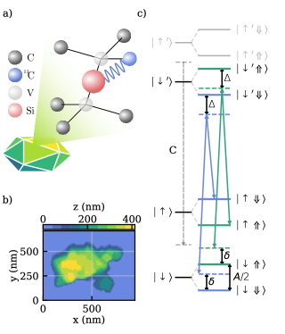
The electronic level scheme of the SiV- consists of four spin-degenerate orbital states, two of which form the ground-state (GS) and excited-state (ES), respectively. As a consequence four optically active transitions arise, which we label as A, B, C and D. For the remainder of the text we only use transition C, for which the spin levels are depicted in FIG. 1 c). The spin degeneracy of the GS and ES levels can be lifted by applying a magnetic field, giving access to an electron spin qubit, e.g the one labeled by and [17, 18]. When using such a spin-qubit at liquid helium temperature, its coherence time is mainly limited through phonon-induced dephasing. The latter can be mitigated by either cooling the system to mK temperatures [11], changing the PDOS [12] or increasing the GS-splitting, which suppresses phonon absorption [19, 20]. The use of NDs is an appealing choice as a host for the SiV-, since they can combine two of the mentioned effects to increase spin-coherence times at temperatures around 4K. The reduced size modifies the PDOS and commonly-present strain in NDs results in an increased GS-splitting. We therefore investigate spectrally shifted SiV- where high strain can be expected [19] and studied them for their optical and spin-coherence properties.
The NDs were coated onto a sapphire substrate with good thermal conductivity. The sample was then cooled to liquid helium temperatures in a continuous flow-cryostat and investigated using a home-built confocal microscope. Four permanent magnets in a Hallbach-configuration designed for an in-plane field strength of around 400 mT were used to lift the spin degeneracy. Individual transitions of the SiV- were addressed by photo-luminescence excitation spectroscopy (PLE).
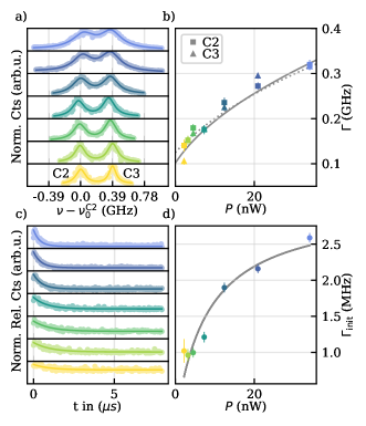
After finding a suitable SiV- the optical linewidths of the two spin-preserving transitions, labeled as C2 and C3, were investigated by PLE with varying power (), as shown in FIG. 2 a). The frequency splitting between C2 and C3 \DTLfetchexportvalueerrorsthekeyspinsplittingrthevalue\DTLfetchexportvalueerrorsthekeyerrspinsplittingrthevalue was determined by a double-Lorentzian fit. FIG. 2 b) shows the fitted power-dependent linewidth of C2 and C3. We extrapolated the linewidth to zero power using , where is the linewidth at zero power and with the saturation power . The fit resulted in and , respectively. The saturation powers turned out as and , respectively. Firstly, is close to Fourier limits for commonly found lifetimes inside NDs, suggesting excellent optical quality. Secondly, the narrow linewidths compared to \DTLfetchexportvalueerrorsthekeyspinsplittingrthevalue allow for a strong drive without significant cross-talk between C2 and C3.
We proceeded by measuring the initialization rate of the spin for each excitation power. To this end, we pumped the population out of a thermal maximally-mixed equilibrium state with a resonant pulse of varying power. The resulting fluorescence, shown in FIG. 2 c), was then fitted with an exponential decay. From the fit, we evaluated the initialization fidelity by comparing the maximum fluorescence at the beginning of the pulse with the fluorescence at the end of the pulse, corresponding to the steady state population under resonant drive.
In addition, the corresponding initialization rates are shown in FIG. 2 d). For the highest power we measured an initialization time of and a fidelity of .
From the power dependence of , we determined the spin-branching ratio by fitting , where and are taken from the previously fitted PLE measurements [21].
Extending the measurement procedure of FIG. 2c) to multiple consecutive resonant pulses with increasing temporal spacing probes the exponentially recovering spin population . Fitting an exponential to the peak intensities in each fluorescence pulse resulted in , which ultimately limits spin coherence. In addition, gives insights on the orientation of the SiV- symmetry axis to the magnetic field, where a misalignment leads to spin-mixing and hence shorter relaxation times. From the relatively short together with the spin-branching we estimate only a moderate alignment.
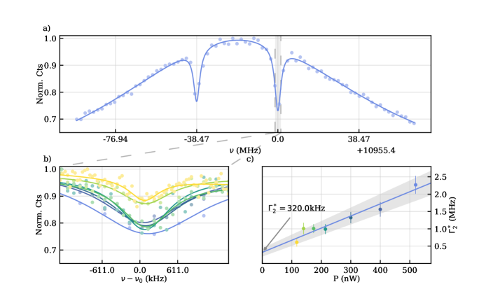
To probe the spin-coherence we used coherent population trapping (CPT). Here, the laser resonantly (, see FIG.1 c)) drove a spin-flipping transition. Simultaneously, an electro-optical modulator (EOM) generated sidebands from which one was swept over the corresponding spin-preserving transition. If the Raman condition () is fulfilled the system is pumped into a dark state quenching the fluorescence signal. For the studied SiV- two dips with a frequency splitting of were present, as shown in FIG.3 a). The splitting is composed of two terms, the parallel coupling term and the perpendicular coupling term . The observed splitting is in close agreement with a theoretically predicted strongly hyperfine-coupled next-nearest neighbor 13C nuclear spin with a coupling strength of [15].
Furthermore, since the dip’s linewidth gives insight on the spin’s dephasing rate, we performed a power dependent measurement, which is shown in FIG. 3 b). Fitting the data with a Lorentzian and extracting the linewidth allowed us to linearly extrapolate the dephasing rate to zero laser power to suppress power-induced broadening. As a result, we obtained a zero-power linewidth of .
This is approximately a ten-fold reduced decoherence rate compared to previously reported measurements in bulk diamond at similar temperatures with [22, 23, 24], and a minor improvement to measurements in a strain-engineered nano-beam, which reported [20, 19].
Combining the latter improvements of spin coherence in high strain environments with the present spin transition frequency of roughly and the spin-preserving transitions’ splitting of suggests a comparably highly strained SiV--center with a GS splitting on the order of 500 GHz [19].
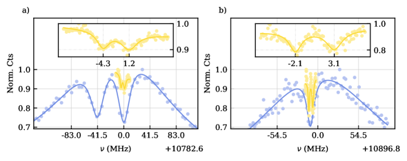
We further investigated the spin environment in the same agglomeration of NDs by performing CPT measurements on different SiV--centers. The measurement revealed coupling of multiple spins, as shown in FIG. 4. For example, the SiV- in FIG 4 a) displayed two dips split by . Measurements with reduced power resolved two more dips, split by as shown in the inset. They exhibited linewidths of and , for the left and right dip, respectively. The distinct linewidths suggest coupling to two other surrounding SiV--centers’ electron spins with coherence properties commonly found with SiV- in low to moderate strain bulk diamond [22, 23, 24]. Assuming a dipolar electron-electron coupling would correspond to a distance on the order of 10 , reasonable for the size of the ND and density of SiV--centers under study.
Another SiV-, displayed in FIG. 4 b), exhibited two individual dips at low optical power with linewidths of and , for the left and right respectively. In contrast to the previous SiV-s’ multi-dip structure with distinct linewidths, the fact that the present SiV- has closely matching and relatively narrow linewidths is indicative of a coupled nearby 13C nuclear spin with a coupling strength of MHz [20]. In this case the distance between the two coupled spins is on the order of [20].
The presented results open up new possibilities to utilize the electron and nuclear spin environment of SiV--centers in NDs as an elementary unit of diamond-based qubits with integrability into photonic platforms, like photonic crystal or open microcavities [25, 16, 26, 14]. The thereby formed hybrid quantum system enables efficient mapping of the quantum state of the electron spin to flying photonic qubits as well as coupling to local memory units consisting of nearby nuclear spins. Our work also suggests that the access to small spin registers is feasible for SiV--centers in NDs. Increasing the GS-splitting beyond 500 GHz, e.g. by hydrostatic pressure [28] might further improve coherence times. Additionally temperatures around 4 K within a flow-cryostat become sufficient. The measured dephasing rates bring coherent control of different spin qubits in NDs, either by means of direct microwave drive [27] or all-optical control using a Raman-type lambda scheme, as has recently been shown for the tin-vacancy [21], into reach. For the system parameters in our measurements, an all-optical Rabi driving strength in the order of several MHz can be expected, comparable to driving rates achieved with microwave driving [27] . Additionally, the high sensitivity enables to detect close-by electron or nuclear spins. Furthermore, with coherent electron spin control, direct [29] or indirect [30] control of a nuclear spin becomes possible. Mapping information of the electron spin to a strongly coupled long-lived nuclear spin establishes SiV--centers in NDs as a viable candidate for an interchangeable hybrid quantum memory.
Acknowledgements.
The authors thank V.A. Davydov for synthesis and processing of the nanodiamond material. The project was funded by the Baden-Württemberg Stiftung in Project Internationale Spitzenforschung. N.L acknowledges support from IQST. A.K. acknowledges support of the BMBF/VDI in the Projects HybridQToken (16KISQO43K), QR.X (16KISQ006) and Spinning (13N16215). The authors acknowledge funding by the European Union and the DFG within the Quantera-project SensExtreme.References
- Kimble [2008] H. J. Kimble, The quantum internet, Nature 453, 1023 (2008).
- Wehner et al. [2018] S. Wehner, D. Elkouss, and R. Hanson, Quantum internet: A vision for the road ahead, Science 362, 6412 (2018).
- Briegel et al. [1998] H.-J. Briegel, W. Dür, J. I. Cirac, and P. Zoller, Quantum repeaters: The role of imperfect local operations in quantum communication, Phys. Rev. Lett. 81, 5932 (1998).
- Childress et al. [2006] L. Childress, J. M. Taylor, A. S. Sørensen, and M. D. Lukin, Fault-tolerant quantum communication based on solid-state photon emitters, Phys. Rev. Lett. 96, 070504 (2006).
- Pompili et al. [2021] M. Pompili, S. L. N. Hermans, S. Baier, H. K. C. Beukers, P. C. Humphreys, R. N. Schouten, R. F. L. Vermeulen, M. J. Tiggelman, L. dos Santos Martins, B. Dirkse, S. Wehner, and R. Hanson, Realization of a multinode quantum network of remote solid-state qubits, Science 372, 259 (2021).
- Faraon et al. [2012] A. Faraon, C. Santori, Z. Huang, V. M. Acosta, and R. G. Beausoleil, Coupling of nitrogen-vacancy centers to photonic crystal cavities in monocrystalline diamond, Phys. Rev. Lett. 109, 033604 (2012).
- Chu et al. [2014] Y. Chu, N. de Leon, B. Shields, B. Hausmann, R. Evans, E. Togan, M. J. Burek, M. Markham, A. Stacey, A. Zibrov, A. Yacoby, D. Twitchen, M. Loncar, H. Park, P. Maletinsky, and M. Lukin, Coherent optical transitions in implanted nitrogen vacancy centers, Nano Letters 14, 1982 (2014), pMID: 24588353, https://doi.org/10.1021/nl404836p .
- Rogers et al. [2014a] L. J. Rogers, K. D. Jahnke, T. Teraji, L. Marseglia, C. Müller, B. Naydenov, H. Schauffert, C. Kranz, J. Isoya, L. P. McGuinness, and F. Jelezko, Multiple intrinsically identical single-photon emitters in the solid state, Nature Communications 5, 4739 (2014a).
- Sipahigil et al. [2014] A. Sipahigil, K. D. Jahnke, L. J. Rogers, T. Teraji, J. Isoya, A. S. Zibrov, F. Jelezko, and M. D. Lukin, Indistinguishable photons from separated silicon-vacancy centers in diamond, Phys. Rev. Lett. 113, 113602 (2014).
- Waltrich et al. [2023] R. Waltrich, M. Klotz, V. N. Agafonov, and A. Kubanek, Two-photon interference from silicon-vacancy centers in remote nanodiamonds, Nanophotonics 12, 3663 (2023).
- Sukachev et al. [2017] D. D. Sukachev, A. Sipahigil, C. T. Nguyen, M. K. Bhaskar, R. E. Evans, F. Jelezko, and M. D. Lukin, Silicon-vacancy spin qubit in diamond: A quantum memory exceeding 10 ms with single-shot state readout, Phys. Rev. Lett. 119, 223602 (2017).
- Klotz et al. [2022] M. Klotz, K. G. Fehler, R. Waltrich, E. S. Steiger, S. Häußler, P. Reddy, L. F. Kulikova, V. A. Davydov, V. N. Agafonov, M. W. Doherty, and A. Kubanek, Prolonged orbital relaxation by locally modified phonon density of states for the center in nanodiamonds, Phys. Rev. Lett. 128, 153602 (2022).
- Fehler et al. [2020] K. G. Fehler, A. P. Ovvyan, L. Antoniuk, N. Lettner, N. Gruhler, V. A. Davydov, V. N. Agafonov, W. H. Pernice, and A. Kubanek, Purcell enhanced emission from individual siv center in nanodiamonds coupled to a si3n4 based photonic crystal cavity, Nanophotonics 9, 3655 (2020).
- Fehler et al. [2021] K. G. Fehler, L. Antoniuk, N. Lettner, A. P. Ovvyan, R. Waltrich, N. Gruhler, V. A. Davydov, V. N. Agafonov, W. H. P. Pernice, and A. Kubanek, Hybrid quantum photonics based on artificial atoms placed inside one hole of a photonic crystal cavity, ACS Photonics 8, 2635 (2021), https://doi.org/10.1021/acsphotonics.1c00530 .
- Nizovtsev et al. [2020] A. P. Nizovtsev, S. Y. Kilin, A. L. Pushkarchuk, S. A. Kuten, N. A. Poklonski, D. Michels, D. Lyakhov, and F. Jelezko, Spatial and Hyperfine Characteristics of SiV– and SiV0 Color Centers in Diamond DFT Simulation, Semiconductors 54, 1685 (2020).
- Bayer et al. [2023] G. Bayer, R. Berghaus, S. Sachero, A. B. Filipovski, L. Antoniuk, N. Lettner, R. Waltrich, M. Klotz, P. Maier, V. Agafonov, et al., Optical driving, spin initialization and readout of single siv- centers in a fabry-perot resonator, Communications Physics 6, 300 (2023).
- Hepp et al. [2014] C. Hepp, T. Müller, V. Waselowski, J. N. Becker, B. Pingault, H. Sternschulte, D. Steinmüller-Nethl, A. Gali, J. R. Maze, M. Atatüre, and C. Becher, Electronic structure of the silicon vacancy color center in diamond, Phys. Rev. Lett. 112, 036405 (2014).
- Rogers et al. [2014b] L. J. Rogers, K. D. Jahnke, M. W. Doherty, A. Dietrich, L. P. McGuinness, C. Müller, T. Teraji, H. Sumiya, J. Isoya, N. B. Manson, and F. Jelezko, Electronic structure of the negatively charged silicon-vacancy center in diamond, Phys. Rev. B 89, 235101 (2014b).
- Meesala et al. [2018] S. Meesala, Y.-I. Sohn, B. Pingault, L. Shao, H. A. Atikian, J. Holzgrafe, M. Gundogan, C. Stavrakas, A. Sipahigil, C. Chia, R. Evans, M. J. Burek, M. Zhang, L. Wu, J. L. Pacheco, J. Abraham, E. Bielejec, M. D. Lukin, M. Atatüre, and M. Lončar, Strain engineering of the silicon-vacancy center in diamond, Phys. Rev. B 97, 205444 (2018).
- Sohn et al. [2018] Y.-I. Sohn, S. Meesala, B. Pingault, H. A. Atikian, J. Holzgrafe, M. Gündoğan, C. Stavrakas, M. J. Stanley, A. Sipahigil, J. Choi, M. Zhang, J. L. Pacheco, J. Abraham, E. Bielejec, M. D. Lukin, M. Atatüre, and M. Lončar, Controlling the coherence of a diamond spin qubit through its strain environment, Nature Communications 9, 2012 (2018).
- Debroux et al. [2021] R. Debroux, C. P. Michaels, C. M. Purser, N. Wan, M. E. Trusheim, J. Arjona Martínez, R. A. Parker, A. M. Stramma, K. C. Chen, L. de Santis, E. M. Alexeev, A. C. Ferrari, D. Englund, D. A. Gangloff, and M. Atatüre, Quantum control of the tin-vacancy spin qubit in diamond, Phys. Rev. X 11, 041041 (2021).
- Rogers et al. [2014c] L. J. Rogers, K. D. Jahnke, M. H. Metsch, A. Sipahigil, J. M. Binder, T. Teraji, H. Sumiya, J. Isoya, M. D. Lukin, P. Hemmer, and F. Jelezko, All-optical initialization, readout, and coherent preparation of single silicon-vacancy spins in diamond, Phys. Rev. Lett. 113, 263602 (2014c).
- Becker et al. [2018] J. N. Becker, B. Pingault, D. Groß, M. Gündoğan, N. Kukharchyk, M. Markham, A. Edmonds, M. Atatüre, P. Bushev, and C. Becher, All-optical control of the silicon-vacancy spin in diamond at millikelvin temperatures, Phys. Rev. Lett. 120, 053603 (2018).
- Pingault et al. [2014] B. Pingault, J. N. Becker, C. H. H. Schulte, C. Arend, C. Hepp, T. Godde, A. I. Tartakovskii, M. Markham, C. Becher, and M. Atatüre, All-optical formation of coherent dark states of silicon-vacancy spins in diamond, Phys. Rev. Lett. 113, 263601 (2014).
- Antoniuk et al. [2023] L. Antoniuk, N. Lettner, A. P. Ovvyan, S. Haugg, M. Klotz, H. Gehring, D. Wendland, V. N. Agafonov, W. H. P. Pernice, and A. Kubanek, All-optical spin initialization via a cavity broadened optical transition in on-chip hybrid quantum photonics (2023), arXiv:2308.15544 [quant-ph] .
- Nguyen et al. [2019] C. T. Nguyen, D. D. Sukachev, M. K. Bhaskar, B. Machielse, D. S. Levonian, E. N. Knall, P. Stroganov, C. Chia, M. J. Burek, R. Riedinger, H. Park, M. Lončar, and M. D. Lukin, An integrated nanophotonic quantum register based on silicon-vacancy spins in diamond, Phys. Rev. B 100, 165428 (2019).
- Pingault et al. [2017] B. Pingault, D.-D. Jarausch, C. Hepp, L. Klintberg, J. N. Becker, M. Markham, C. Becher, and M. Atatüre, Coherent control of the silicon-vacancy spin in diamond, Nat Commun 8, 15579 (2017), number: 1 Publisher: Nature Publishing Group.
- Vindolet et al. [2022] B. Vindolet, M.-P. Adam, L. Toraille, M. Chipaux, A. Hilberer, G. Dupuy, L. Razinkovas, A. Alkauskas, G. Thiering, A. Gali, et al., Optical properties of siv and gev color centers in nanodiamonds under hydrostatic pressures up to 180 gpa, Physical Review B 106, 214109 (2022).
- Stas et al. [2022] P.-J. Stas, Y. Q. Huan, B. Machielse, E. N. Knall, A. Suleymanzade, B. Pingault, M. Sutula, S. W. Ding, C. M. Knaut, D. R. Assumpcao, Y.-C. Wei, M. K. Bhaskar, R. Riedinger, D. D. Sukachev, H. Park, M. Lončar, D. S. Levonian, and M. D. Lukin, Robust multi-qubit quantum network node with integrated error detection, Science 378, 557 (2022), https://www.science.org/doi/pdf/10.1126/science.add9771 .
- Vallabhapurapu et al. [2022] H. H. Vallabhapurapu, C. Adambukulam, A. Saraiva, and A. Laucht, Indirect control of the nuclear spin in diamond, Phys. Rev. B 105, 205435 (2022).