Nonlinear kinetic inductance sensor
Abstract
The concept of nonlinear kinetic inductance sensor (NKIS) of electromagnetic radiation is proposed. The idea is based on divergency of kinetic inductance ( is a momentum of superconducting electrons, is a supercurrent) of hybrid superconductor/normal metal (SN) bridge at current ( is a depairing current of the hybrid) and temperature much smaller than critical temperature . It makes possible to have large change of phase difference along SN bridge in current biased regime at even for small electron temperature increase. Appearance of is accompanied by the change of the current and magnetic flux through the coupled superconducting ring which could be measured with help of superconducting quantum interference device (SQUID). In some respect proposed sensor may be considered as a superconducting counterpart of transition edge sensor (TES) those work is based on large derivative ( is a resistance) near . Because at SN bridge is in gapless regime there is no low boundary for frequency of detected e.m. radiation. Our calculations show that such a sensor can operate in single photon regime and detect single photons with frequency 10 GHz. We argue that the nontrivial dependence of SN bridge could be also used in detectors of continuous e.m. radiation, current and magnetic field sensors.
I Introduction
Superconductors are widely used in our days as a basic element of detector/sensor of electromagnetic radiation. Absorbed photons create quasiparticles and/or increase their energy in superconductors and it changes its superconducting/transport properties. For example in kinetic inductance detector (KID) Zmuidzinas_2012 and transition edge sensor (TES) Irwin_2005 kinetic inductance and resistance increases, correspondingly, work of superconductor-insulator-superconductor (SIS) mixer is based on change of its highly nonlinear current-voltage characteristic Gundlach_2000 , while in superconducting nano- and microstrip single photon detectors (SSPD) current carrying superconducting strip switches to the resisitive/normal state after appearance of hot spot (region with heated electrons) in the place where photon is absorbed Natarajan_2012 .
In case of TES its high sensitivity is based on narrow resistive transition of superconductor near critical temperature and usage of superconducting quantum interference device (SQUID) to measure response of the detector - the larger derivative the larger resistance and current change via voltage-biased superconductor. One of the advantages of TES is that it operates in resistive state near and, hence, superconducting gap practically vanishes, which means that there is no low boundary typical for KID or SSPD where energy of the photon should exceed twice the superconducting energy gap . Besides it can work in single photon regime (for infra-red and photons with larger energy) and resolve energy of the absorbed photon contrary to SSPD.
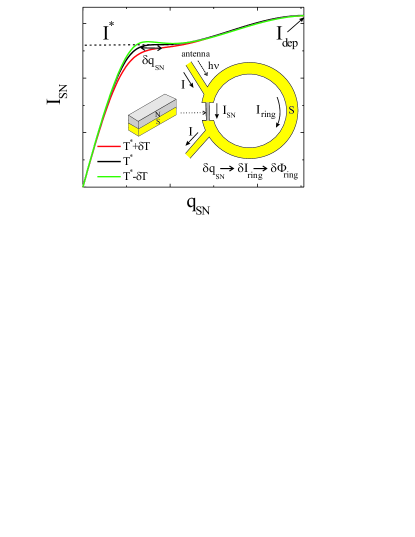
Here we offer another type of energy resolved sensor which as a TES is based on large variations of transport properties due to small temperature increase of the whole superconducting detecting element. Contrary to TES it operates in superconducting state at but despite that it has zero superconducting gap. The proposed nonlinear kinetic inductance sensor (NKIS) consists of current biased hybrid superconductor-normal metal (SN) bridge coupled to superconducting ring (see Fig. 1). SN bridge has unique dependence of supercurrent (throughout the paper we use absolute value of the current) on momentum . At there is a ’plateau’ on dependence at where kinetic inductance diverges ( is a length of SN bridge). At ’plateau’ transforms to part of with finite slope and finite . Therefore one may have large change of and phase difference by biasing of SN bridge at and bath temperature even in case of small increase of electron temperature. Increase of leads to increase of the current in superconducting ring and magnetic flux through it. The last change could be measured by SQUID. We assume that SN bridge and ring are parts of the antenna which receives the photon and photon can be absorbed only in SN bridge which is in gapless regime at and in the rest of the system .
In comparison with TES where the large derivative provides large change of the current, in NKIS the large derivative provides the large change of . In contrast to TES proposed NKIS operates in superconducting, dissipation less state, and at and which potentially may lead to larger sensitivity than TES has. Like a TES it also does not have low boundary for photon detection because at current the superconducting gap is equal to zero in SN bridge. Below we show that NKIS can potentially detect even single photons with 10-30 GHz when it is biased at temperature .
II Nonlinear kinetic inductance sensor
In this section we present results of our calculations which demonstrate detection ability of NKIS in single photon regime. In Fig. 2(a) we show dependence at different temperatures for SN hybrid bridge having following parameters: thicknesses of S and N layers , (), ratio of diffusion coefficients , is the momentum of Cooper pairs ( is the phase of superconducting order parameter, A is a vector potential, is a magnetic flux quantum), is the critical temperature and is a depairing current at of single S layer. To find it we use one-dimensional Usadel model (equations and method of calculation are present in Marychev_2021 ) where we take into account dependence of superconducting properties only across thickness of SN bridge and assume that along its length () and across the width (, is a Pearl penetration depth) current density is distributed uniformly.
At temperature near on dependence there is a ’plateau’ at current . It occurs due to temperature driven transition from having one maximum at high T to dependence having two maxima at low T. Maximum at low appears due to increased contribution of N layer to total supercurrent (proximity induced superconductiviy in N layer becomes ’stronger’), which also leads to increase of the slope at small and smaller kinetic inductance. Because N layer has larger diffusion coefficient the depairing effect of supervelocity (in Usadel equation it is described by term with ) is larger in N layer than in S layer ( across the thickness of SN bridge). It leads to suppression of superconductivity in N layer at smaller than in S layer and need to increase momentum to keep the same supercurrent which results in appearance of the ’plateau’.
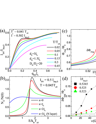
Fig. 2(b) demonstrates that at the superconductivity in SN bridge is gapless. We discuss gapless regime in details below and here only notice that although gap is zero but density of states in large part of S layer is much smaller than in the normal state at . We estimate the effective ’normal’ thickness of the SN bridge where density of states is close to normal state value as .
When SN bridge is connected with a superconducting ring the total current consists of and (see Fig. 1). We assume that the ring is made of the same material as S layer of SN bridge and it has the same thickness but its width is much larger than the width of SN bridge: . Because of small thicknesses and widths of SN bridge and ring we may neglect screening effects and assume that . From condition that over the ring perimeter and SN bridge (we assume there is no fluxoid inside the ring) we find: . With this relation and definition we may write expression for the total current:
| (1) |
where we use linear dependence (because ) and weak temperature dependence of depairing current of S layer at .
With known dependence and expression for magnetic flux through the ring ( is geometric inductance of the ring, R is its radius, and is a magnetic constant) we find dependence . We show it in Fig. 2(c) for different temperatures and following parameters: , , , , , (=19.5 nm, =30,6 A, ). Material parameters of superconductor are typical for granular Al Levy-Bertrand_2019 and close to parameters of other high resistive low temperature superconductors like TiN Leduc_2010 , PtSi Szypryt_2016 or Hf Coiffard_2020 . We also choose Cu as a material for N layer.
In the following we consider ability of NKIS detect single photons (analysis can be also made when there is continuous flux of e.m. radiation, as it was done in Giazotto_2008 ). Using above results we find dependence on change of the temperature of SN bridge after absorption of the single photon with energy - see Fig. 2(d). We relate with with help of energy conservation law
| (2) |
where is a heat capacity of electrons, is bath temperature and is a volume of SN bridge where density of electron states is close to its normal state value. We also neglect heating of phonons due to their much smaller heat capacity and use in calculations which corresponds to Cu.
The important characteristic of photon sensor is the signal to noise ratio . Noise may be estimated as where is the flux sensitivity of the dc SQUID and is its bandwidth Giazotto_2008 . With (which is ten times larger than the value reported in Kiviranta_2004 ) and we find . Therefore with a magnitude of signal the ratio .
In Fig. 2(d) level is marked by dashed line and our results demonstrate that proposed sensor could be able to detect single photons with when it is biased at and current .
The same sensor could be used to detect single THz and subTHz photons. Because of their much larger energy we do not need mK temperatures and . Note that and for superconductor those thickness scales with . Therefore our results could be easily rescaled - one needs to multiply in Fig. 2(d) by and by . For example for superconductor with (NbN, NbTiN) absorption of photon with at leads to change of magnetic flux by while 30 GHz photon changes magnetic flux by .
After photon absorption electrons are heated on and than cool down due to electron-phonon interaction on time scale . In proposed system there is no cooling of electrons by diffusion due to large energy gap on the ends of the SN bridge where it is attached to superconductor with large gap . At low temperature and for example for Ag it could be as large as in temperature range 10-100 mK Giazotto_2008 . We expect that similar values are valid for Cu too.
III Current controlled energy gap
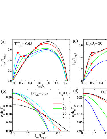
In this section we discuss gapless regime in SN bridge. In ordinary ’dirty’ superconductor energy gap is finite even at where it is about of Maki_1963 ( is the energy gap at zero current). However in SN bridge gap goes to zero at which is marked by red circles in Fig. 3. Gapless state in SN bridge is possible due to large difference between diffusion coefficients in N and S layers. As we discuss earlier pair breaking effect due to finite momentum in ’dirty’ superconductor is described by term in Usadel equation and when gap vanishes in ordinary superconductor Maki_1963 . Roughly the same criteria is valid in SN bilayer which one can see from Fig. 3(a) where with increase of gap closes at smaller value of momentum .
In ordinary superconductor condition is fulfilled on unstable branch of dependence and superconducting order parameter rapidly decreases with increase of . In SN bilayer gapless state is stable due to presence of S layer having much smaller diffusion coefficient and, hence, much larger .
IV ’Plateau’ at different parameters of SN bridge
We find that the ’plateau’ exists in wide range of parameters of SN bridge. With increase of (keeping and ratio the same) temperature , width of ’plateau’ and ratio decrease (see panel (a) in Fig. 4). We also find that there is minimal critical thickness (for example it is about of for and ) below which ’plateau’ does not exist at any temperature. Panel (b) illustrates that it is necessary to have large ratio to have a ’plateau’ (we find parameters when it exists for but in this case which makes impractical its usage). Another they to control is to change thickness of N layer and finite interface transparency for electron motion between S and N layers. For example increase of or decrease of transparency shifts to lower temperatures because in this case proximity induced superconductivity in N layer becomes ’weaker’ and one needs smaller T to enhance it.
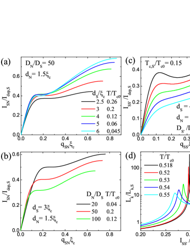
The ’plateau’ on may also exist in bilayer composed of two superconductors having different critical temperatures - see Fig. 4(c). Again gapless regime is realized at and dependence is sensitive to small variations of temperature. The sensitivity to temperature is well visible in Fig. 4(d) where we plot current dependent kinetic inductance. With decrease of the temperature peak appears on dependence which becomes sharp at and .
V Discussion
Peak on dependence has been observed recently for MoN(40nm)/Cu(40nm) strip (, ) Levichev_2023 . With lowering of temperature width of the peak decreases while amplitude increases in accordance with prediction of Usadel model. In that experiment the critical current was smaller than depairing current (most probably due to edge defects) because divergency of has not been found at Levichev_2023 . The thickness of studied sample was optimized to observe finite momentum superconductivity at relatively small in-plane magnetic field and narrow peak should appear at , as Usadel model predicts, which is much lower than the minimal reached temperature in that experiment.
Single microwave photon detectors based on heating of small volume superconductor have been proposed earlier. The similar design as in Fig. 1 but with SNS Josephson junction (JJ) instead of SN bridge was discussed in Ref. Giazotto_2008 . Authors of that work offer to exploit strong temperature dependence of critical current of long JJ and they predict that such a device would be able to detect THz photons. In superconducting loop with two SNS junctions heating of one JJ by absorbed photon produces voltage pulse (when magnetic flux through the loop is close to ) and it is idea of another type of single THz photon detector Solinas_2018 . In Ref. Paolucci_2023 more complicated design was studied with two coupled superconducting loops (one with magnetic flux and another with ) and two (short and long) SNS Josephson junctions. It is assumed that microwave photon is absorbed in long JJ and it leads to the measurable change of quasiparticle current via tunnel junction connected with short JJ - for that device ability to detect photons in range 10 GHz-10 THz was predicted. In Astafiev_2022 the change of impedance of SN bridge placed in the end of superconducting coplanar line serves as a signal that microwave photon is absorbed there and this device does not need external current drive.
In comparison with Refs. Giazotto_2008 ; Solinas_2018 ; Paolucci_2023 our system has more simple design and it is not based on usage of SNS junction. As for the system from Astafiev_2022 it is possible to vary parameters of SN bridge (width, length, thickness of N layer) to match NKIS with 50 microwave impedance of the coplanar feed line when it is needed. Due to similarity with TES it is possible to use experience and methods which has been developed for that device. In comparison with TES the advantage of NKIS is that it operates in superconducting state. But more important that there is a current and temperature where and at which is consequence of temperature driven ’phase transition’ from dependence having one maximum to having two maxima and appearance of the extremum at small near which changes sign.
In reality peak in dependence will be smeared due to temperature/current fluctuations, local variations of thickness/width and/or material parameters (local , resistivity, etc.) of the sample which are also responsible for broadening of resistive transition in TES. However in contrast to resistive transition where always and is reversible on dependence at there is a region with near (see Fig. 1). It implies hysteretic behavior of near . If we choose temperature slightly below increase of electron temperature leads to jump of and which is easy to detect. But after cooling of electrons SN bridge does not return to initial state which is not convenient for following detection process. In this case fluctuations help to come back to the initial state while change of remains large. In some respect situation is similar to current-voltage characteristics (IVC) of superconducting bridge. Usually at IVC is smooth and reversible while at it is hysteretic with abrupt voltage jump at . Somewhere in between there is temperature when IVC is reversible but with large at . We expect something similar effect at but for dependencies and near .
Although we mainly concentrate on ability to detect single microwave photon the NKIS can also work in continuous regime like TES (hot electron bolometer). In this case to find one has to solve balance equation which includes heating of SN bridge due to absorbed e.m. radiation and its cooling due to electron-phonon interaction. Note, that for this type of application is not necessary to use SQUID readout and small size SN bridge. As in KID one may use coplanar waveguide with capacitively coupled superconducting circuit which contains current biased SN bridge. Biased at and SN bridge drastically changes its kinetic inductance when temperature increases (see evolution of with temperature in Fig. 4(d)). Due to gapless superconductivity quality factor of a superconducting circuit should be small in comparison with ordinary KID which means broadening of the resonance but it could be compensated by extremely large change of .
Divergency of at could be also used in current and magnetic field sensors. Indeed, even small deviation of the current from leads to large change of at temperature close to - see Fig. 4(d). This property could be used in kinetic inductance parametric up-converter Kher_2016 to amplify small current signal in TES instead of SQUID and kinetic inductance magnetometer Luomahaara_2014 to measure screening current produced by magnetic field.
Acknowledgements.
The work is supported by the Ministry of Science and Higher Education of the Russian Federation (contract no. 075-15-2022-316 with the Photonics Center of Excellence).References
- (1) J. Zmuidzinas, Superconducting microresonators: Physics and applications, Annu. Rev. Condens. Matter Phys. 3, 169 (2012).
- (2) K. Irwin, G. Hilton, Transition-Edge Sensors. In: C. Enss (editor) Cryogenic Particle Detection. Topics in Applied Physics, Springer, Berlin, Heidelberg, 99 p.63 (2005).
- (3) K. H. Gundlach and M. Schicke, SIS and bolometer mixers for terahertz frequencies, Supercond. Sci. Technol. 13, R171 (2000).
- (4) C. M. Natarajan, M. G. Tanner, and R. H. Hadfeld, Superconducting nanowire single-photon detectors: physics and applications, Supercond. Sci. Technol. 25, 063001 (2012).
- (5) P. M. Marychev and D. Yu. Vodolazov, Extraordinary kinetic inductance of superconductor/ferromagnet/normal metal thin strip in an Fulde-Ferrell state, J. Phys.: Condens. Matter 33, 385301 (2021).
- (6) F. Levy-Bertrand, T. Klein, T. Grenet, O. Dupre, A. Benoiot, A. Bideaud, O. Bourrion, M. Calvo, A. Catalano, A. Gomez, J. Goupy, L. Grunhaupt, U. v. Luepke, N. Maleeva, F. Valenti, I. M. Pop, and A. Monfardini, Electrodynamics of granular aluminum from superconductor to insulator: Observation of collective superconducting modes, Phys. Rev. B 99, 094506 (2019).
- (7) H. G. Leduc, B. Bumble, P. K. Day, B. Ho Eom, J. Gao, S. Golwala, B. A. Mazin, S. McHugh, A. Merrill, D. C. Moore, O. Noroozian, A. D. Turner, and J. Zmuidzinas, Titanium nitride films for ultrasensitive microresonator detectors, Appl. Phys. Lett. 97, 102509 (2010).
- (8) P. Szypryt, B. A. Mazin, G. Ulbricht, B. Bumble, S. R. Meeker, C. Bockstiegel, and A. B. Walter, High quality factor platinum silicide microwave kinetic inductance detectors, Appl. Phys. Lett. 109, 151102 (2016).
- (9) G. Coiffard, M. Daal, N. Zobrist, N. Swimmer, S. Steiger, B. Bumble and B. A. Mazin, Characterization of sputtered hafnium thin films for high quality factor microwave kinetic inductance detectors, Supercond. Sci. Technol., 33, 07LT02 (2020).
- (10) F. Giazotto, T. T. Heikkila, G. P. Pepe, P. Helisto, A. Luukanen, and J. P. Pekola, Ultrasensitive proximity Josephson sensor with kinetic inductance readout, Appl. Phys. Lett. 92, 162507 (2008).
- (11) M. Kiviranta, J. S. Penttila, L. Gronberg, J. Hassel, A. Virtanen, and H. Seppa, Design and performance of multiloop and washer SQUIDs intended for sub-kelvin operation, Supercond. Sci. Technol. 17, S285 (2004).
- (12) K. Maki, On Persistent Currents in a Superconducting Alloy. II, Progr. Theoret. Phys. (Kyoto) 29, 333 (1963).
- (13) M. Yu. Levichev, I. Yu. Pashenkin, N. S. Gusev, D.Yu. Vodolazov, Finite momentum superconductivity in superconducting hybrids: Orbital mechanism, Phys. Rev. B 108, 094517 (2023).
- (14) P. Solinas, F. Giazotto, and G. P. Pepe, Proximity SQUID Single-Photon Detector via Temperature-to-Voltage Conversion, Phys. Rev. Appl. 10, 024015 (2018).
- (15) F. Paolucci, Nonlocal Superconducting Single-Photon Detector, Phys. Rev. Appl. 20, 014003 (2023).
- (16) V. Lubsanov, V. Gurtovoi, A. Semenov, E. Glushkov, V. Antonov and O. Astafiev, Materials for a broadband microwave superconducting single photon detector, Supercond. Sci. Technol. 35 105013 (2022).
- (17) A. Kher, P. K. Day, B. H. Eom, J. Zmuidzinas and H. G. Leduc, Kinetic Inductance Parametric Up-Converter, J. Low Temp. Phys. 184, 480 (2016).
- (18) J. Luomahaara, V. Vesterinen, L. Groenberg and J. Hassel, Kinetic inductance magnetometer, Nat. Commun. 5, 4872 (2014).