Optical spectrum of -type and -type monolayer MoS2 in the presence of proximity-induced interactions
Abstract
In this paper, we examined the effects of proximity-induced interactions such as Rashba spin-orbit coupling (SOC) and effective Zeeman fields (EZFs) on the optical spectrum of -type and -type monolayer (ML)-MoS2. The optical conductivity is evaluated using the standard Kubo formula under Random phase approximation (RPA) with including the effective electron-electron interaction. It has been found that there exists two absorption peaks in -type ML-MoS2 and two knife shaped absorptions in -type ML-MoS2 which are contributed by the inter-subband spin flip electronic transitions within conduction and valence bands at valleys and with a lifted valley degeneracy. The optical absorptions in -type and -type ML-MoS2 occur in THz and infrared radiation regimes and the position, height, and shape of them can be effectively tuned by Rashba parameter, EZFs parameters, and carrier density. The interesting theoretical predictions in this study would be helpful for the experimental observation of the optical absorption in infrared to THz bandwidths contributed by inter-subband spin flip electronic transitions in a lifted valley degeneracy monolayer transition metal dichalcogenides (ML-TMDs) system. The obtained results indicate that ML-MoS2 with the platform of proximity interactions make it a promising infrared and THz material for optics and optoelectronics.
I Introduction
In recent years, the discovery of atomically thin two-dimensional (2D) materials such as graphene and monolayer transition metal dichalcogenides (ML-TMDs) has been an important and promising field of research in condensed matter physics Novoselov04 ; Mak10 ; Wang12 . Due to the unique electronic and optical properties for potential applications in next generation of high-performance nanoelectronic devices and unique valleytronic features for information technology Cao12 ; Schaibley16 ; Choi23 , ML-TMDs have attracted much attention for scientific researches. The electronic structure of free-standing ML-TMDs is degenerated in and valleys but with the opposite spin orientations Xu14 . The valley degeneracy of ML-TMDs can also be lifted via the exchange interaction induced by the proximity interaction in the presence of a ferromagnetic substrate Qi15 ; Zhang16 ; Cortes22 ; Zhao20 . The proximity-induced 2D ML-TMD based valleytronic system has also led to the proposal to observe novel optical phenomena such as optical Hall effect and valley Hall effect Zhao20 ; Xiao12 .
The optical and transport properties of ML-MoS2 have been theoretically and experimentally investigated Li12 ; Krstajic16 ; Xiao16 ; Zhao20 ; Cao12 ; Mak12 ; Radisavljevic13 ; Mak10 ; Splendiani10 . Previous theoretical results have indicated that the splittings of the conduction and valence bands of ML-MoS2 in the presence of Rashba spin-orbit coupling (SOC) can introduce optical absorptions in terahertz (THz) to infrared bandwidths Xiao16 . The breaking of inversion symmetry at the surface or interface with the resultant electric field couples to the spin of itinerant electrons is called the Rashba effect Soumyanarayanan16 . The Rashba effect can lead to momentum-dependent splitting of spin bands and would enable spin-flip electronic transitions Azpiroz12 ; Azpiroz13 . It has been shown that the optical properties such as collective excitations and optical conductivity of traditional 2D system can be greatly influenced by the Rashba effect Xu03apl ; Wang05prb ; Yuan05 ; Yang06 ; Ang14 . Moreover, the proximity-induced exchange interaction that introduced the effective Zeeman fields (EZFs) can lift the electronic energy spectrum by breaking the valley degeneracy Qi15 ; Zhao20 . In order to understand the effect of proximity-induced exchange interaction on the optoelectronic property of ML-TMDs, it is necessary to examine the roles played by the Rashba SOC and EZFs.
In this study, we evaluate the dependence of longitudinal optical conductivity on the proximity-induced interactions under the linear polarized radiation field. The absorption spectrum (optical conductivity) is calculated via the Kubo formulism under the standard random-phase approximation (RPA) by including the effective electron-electron interaction. With considering the contributions of inter-subband spin-flip electronic transitions within conduction and valence bands in different valleys, the effects of - and -types doping (for varying carrier density via chemical doping or applying a gate voltage), EZFs, and the Rashba SOC strength on the optical conductivity of ML-MoS2 at low temperature are investigated.
The paper is organized as follows. In Sec. II, the eigenvalues and wavefunctions of ML-MoS2 in the presence of proximity-induced interactions such as EZFs and the Rashba SOC are obtained by solving the Schrödinger equation. The optical conductivity of ML-MoS2 is calculated through the Kubo formulism with the dynamic dielectric function under RPA. The numerical results of optical conductivity for different doping types, carrier density, the strengths of EZFs and Rashba SOC are presented and discussed in Sec. III. The concluding remarks are summarized in Sec. IV.
II Theoretical Framework
In this study, we consider ML-MoS2 placed on a ferromagnetic substrate such as EuO or EuS where the proximity-induced interactions can lead to an enhanced valley splitting and spin-orbit coupling (SOC) Zhao20 . The low-energy effective Hamiltonian is written in the form of a matrix as
| (1) |
where is the electron wavevector along the 2D-plane, , , and . Here, refers to the () valley, with being the lattice parameter and the hopping parameter Cao12 . The intrinsic SOC parameters and are the spin splitting, respectively, at the bottom of the conduction band and at the top of the valence band in the absence of the Rashba SOC Xiao12 ; Sun14 ; Xiao07 ; Chen99 ; Zhu11 , and are effective Zeeman fields experienced by electrons in the conduction band and holes in valence band in the presence of exchange interaction induced by the substrate. is the direct bandgap between the valence and conduction bandsXiao12 ; Lu13 ; Li12 , and with being the Rashba coefficient Kormnyos14 ; Slobodeniuk16 . After solving the Schördinger equation, one can obtain the eigenvalues and eigenfunctions of electrons or holes in ML-MoS2.
The four eigenvalues are the solutions of the diagonalized equation
| (2) |
with
and the corresponding eigenfunctions for electronic states near the and points are
| (3) |
where , ,
and
is the normalization factor. Here, , , and .
Therefore, we consider the carriers in ML-MoS2 as spin-splitting 2D electron gas (2DEG) in the conduction band or 2D hole gas (2DHG) in the valence band with a two band mode. Here, we use a simplified form and for both conduction and valence subbands. With the energy spectrum of a spin-split 2DEG or 2DHG, the electron density-density (-) correlation function can be obtained, in the absence of - screening, as Chen99 ; Mishchenko03
| (4) |
where
| (5) |
is the structure factor. Here, is defined for electronic transition channel from the branch to the branch with = referring to different spin branches. = is for different valley, is the excitation photon energy, and = is the change of electron wavevector during an - scattering event. is the Fermi-Dirac function with being the Fermi energy at zero temperature or chemical potential at a finite temperature. The dynamical RPA dielectric function hereby writes
| (6) |
Here, ==, =, =, and = are defined for different transition channels, = and ( and ) are for intra-band (inter-subband) transitions, =, and = with being the dielectric constant of the material.
The RPA dielectric function can be used to calculate the effective interaction for optical response with different scattering events. In the presence of - interaction, the effective - correlation function becomes
| (7) |
Using the Kubo formula in the absence of electronic scattering centers (such as impurities and phonons), the optical spectrum or optical conductivity of a spin-valley-splitting 2DEG (2DHG) can be calculated through Yuan05 ; Mishchenko03
| (8) |
In the present study, is induced by current-current correlation via electron-electron interaction with the external electromagnetic field, which normally does not change the wavevector for a carrier. In the long-wavelength limit () and low temperature ( K), the intra-band electronic transitions would not contribute to the optical conductivity. Moreover, strong optical absorptions can occur via inter-subband spin-flip transitions, especially for transitions from an energy lower spin branch to an energy higher spin branch at and valleys.
III Results and discussions
In numerical calculations, we consider the case at low temperature ( K) to calculate the optical conductivity and take the following parameters for ML-MoS2 with ÅeV, eV, meV, and meV Li12 ; Ochoa13 . Usually, the Rashba parameter depends on the type of the substrate and can also be tuned through, e.g., applying a gate voltageYao17 . A large Rashba parameter = meV was found in ML-MoTe2 placed on an EuO substrate Qi15 . The EZFs factors and also depend on the types of substrates Liang17 . For -type ML-MoS2, we take the spin relaxation time for inter-subband spin-flip transitions as 3 and 300 ps for -type ML-MoS2 Yang13 . With the energy relation approximation, one can replace the function in Eq. (4) with a Lorentzian distribution: , where is the width of the distribution Stille12 . It should be noted that energy relaxation time is a frequency-dependent parameter and is usually set to a constant for numerical calculation Nicol08 . We take the dielectric constants for air, bare ML-MoS2 sheet, and bare EuO substrate as , Paul22 , and Leroux-Hugon72 , respectively. The chemical potential for electrons in -type and holes in -type ML-MoS2 can be determined through
| (9) |
and
| (10) |
respectively. As we know, the longitudinal optical conductivity of ML-MoS2 on a ferromagnetic substrate in the presence of proximity-induced interactions can be measured by the infrared spectroscopy and THz TDS measurement. The theoretical model in this study provides an excellent platform to examine the optical absorption property by tuning the parameter such as Rashba parameter , EZFs and , and carrier density.
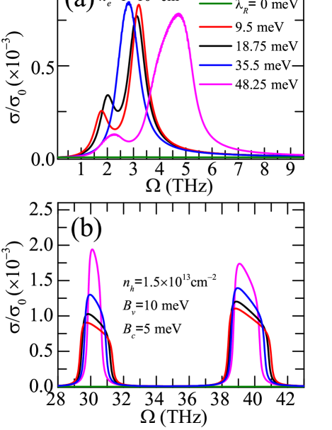
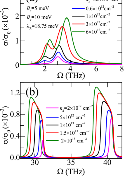
In Fig. 1, we plot the optical conductivity of -type and -type ML-MoS2 as a function of radiation frequency at fixed carrier density cm-2 for electrons and cm-2 for holes, meV, and meV for different Rashba parameters . In Fig. 1(a), we find that there exist two absorption peaks where the lower left peak is induced by spin-flip electronic transitions within valley and the higher right peak is attributed to spin-flip electronic transitions within valley. With increasing , for meV, the lower left absorption peak blueshifts to higher frequencies and the higher right peak redshifts to lower frequencies. For meV, there is only one absorption peak because the band structure is valley degenerated in this case. While for meV, the higher peak redshifts to lower frequencies and the lower peak blueshifts to higher frequencies with increasing . In Fig. 1(b), there are two roughly knife shaped spectral absorptions in the infrared regime. With increasing , the widths of the knife shaped absorptions decrease and the heights of the knife shaped absorptions increase. In the absence of Rashba effect ( meV), we notice that the optical conductivity approaches to zero because the spin-flip transitions are prohibited in this case.
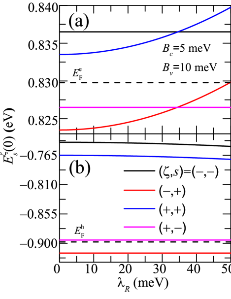
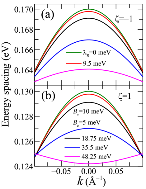
The interesting findings in Fig. 1(a) can be understood with the help of Fig. 2(a) where we show the lowest energies at the bottom of four conduction subbands as a function of Rashba parameter for fixed EZFs meV and meV. With increasing , the energy spacing in valley becomes larger and the energy spacing in valley decreases, which would result in the blueshifts and redshifts of the two absorption peaks. In Fig. 2(b), we show the highest energies at the top of four valence subbands as a function of Rashba parameter for fixed EZFs meV and meV. As we can see, the Rashba parameter affects slightly the top points of them. At a fixed carrier density, we can see that the Fermi level for electrons/holes depends weakly on Rashba parameter, which are in line with the situation we had discussed previously Xiao16 . Thus, the modification of the band structure by the Rashba effect would change the energy spacing between spin splitting subbands near the Fermi level and would result in the tuning of absorption peaks or knife shapes in Fig. 1. In Fig. 3, we also plot the energy spacing between two spin splitting subbands in the valence band for and valleys to clearly clarify the Rashba effect on -type sample. The Rashba effect would affect the energy spacing between the spin splitting valence subbands. With increasing , the region of energy spacing near the Fermi level becomes narrower. Thus, the knife shaped spectral absorptions in Fig. 1(b) also get narrower with increasing . The right boundaries of the two knife shape absorptions correspond to the highest energies in Figs. 3(a)-(b) for the largest electronic transition energies required by optical absorptions in -type sample. As we can see, the regions and values of energy spacings in Fig. 3(a) are larger and higher than those in Fig. 3(b). As a consequence, the left and right knife shaped absorptions in Fig. 1(b) are contributed by the spin-flip electronic transitions in valleys and , respectively, and the right knife shaped absorption is more wider than the left one. The strengths of the knife shaped absorptions also increase with increasing . It should be noted that the electronic band structure in ML-MoS2 modified by EZFs and Rashba SOC have some differences from traditional 2DEG or 2DHG system in the presence of Rashba effect. Thus, the optical spectrum has both commons and differences with traditional 2DEG and 2DHG Ang14 ; Yuan05 . In general, the Rashba effect can play an important and peculiar role in affecting and tuning the optical absorptions in THz and infrared bandwidths for - and -type ML-MoS2 in the presence of proximity-induced exchange interaction.
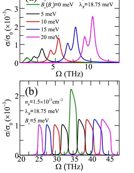
The optical conductivity of - and -type ML-MoS2 is shown in Fig. 4 as a function of radiation frequency at fixed carrier density and for different EZFs. In Fig. 4(a), with a fixed = 10 meV, we find that the width of absorption regime in optical conductivity curve increases and both of the two absorption peaks blueshift with increasing . The strengths of two absorption peaks also become stronger with increasing . For meV, there exists only one peak because the conduction bands in and valleys are degenerated in this case. For the optical spectrum for -type ML-MoS2 shown in Fig. 4(b), there is only one knife shape absorption when meV because of the valley degeneracy of valence bands in and valleys. For meV, there are two knife shape absorptions. With increasing , the left knife shape absorption redshifts and the width of it becomes more narrower. Meanwhile, the right one blueshifts and the width of it becomes more broader.
In Fig. 5, we plot the optical conductivity of -type and -type ML-MoS2 as a function of radiation frequency for fixed meV, EFZs meV and meV for different carrier densities. For ML-MoS2, -type and -type doping samples can be realized through the field effect with different source and drain contacts Chuang14 ; Radisavljevic13 and the doping levels can be tuned through, e.g., applying a gate voltage. Usually, one can reach high carrier density in experiment Chuang14 ; Cuong14 and we choose the carrier density with a magnitude of cm-2 and hole density cm-2 in our numerical calculation. In Fig. 5(a), we can see that both of the two absorption peaks have blueshifts to higher frequencies and the strengths of them become stronger with increasing electron density . Two knife shaped absorptions in Fig. 5(b) become wider and their left boundaries move to the low frequency region with increasing hole density . The left boundaries of two knife shape absorptions are redshifts with increasing carrier density because the chemical potential for holes in -type sample decreases which allows the spin-flip transitions in the lower frequency regime. The width of the right knife shaped absorption in Fig. 5(b) is wider than the left one because the region of energy spacing in valley is larger than in valley . The interesting findings in Fig. 5 are due to the Pauli blockade effect with changing the carrier density Krenner06 . These theoretical results show that the optical absorption of ML-MoS2 in THz and infrared regimes can also be effectively tuned by varying the carrier density.
It should be noted that in our present study, the optical spectrum is mainly determined by electronic transitions through - interaction at low temperature which is an ideal case where the electronic scattering mechanisms (e.g., impurities and phonons) are not taken into account. However, the shape and amplitude of optical conductivity could be also affected by impurity or electron-phonon scattering with the modification of self-energy Li13 .
IV Conclusions
In this paper, we have investigated the infrared to THz optical absorption property of - and -types ML-MoS2 in the presence of proximity-induced interactions such as Rashba SOC and exchange interaction. The optical conductivity is evaluated using the standard Kubo formula under RPA by including the effective electron-electron interaction. We have examined the roles of proximity-induced interactions in affecting optical absorptions occurring in different valleys for both - and -type ML-MoS2. The main conclusions obtained from this study are summarized as follows.
In the presence of proximity-induced interactions, there exist two absorption peaks in -type ML-MoS2 and two knife shaped absorptions in -type ML-MoS2 which are contributed by the inter-subband spin-flip electronic transitions at valleys and with a lifted valley degeneracy. The height and position of the absorption peaks in -type ML-MoS2 can be effectively tuned by Rashba parameter, EFZs parameter , and electron density. The width, height, and position of the knife shaped absorptions in -type ML-MoS2 depend strongly on the Rashba parameter, EFZs parameter , and carrier density. These features in optical conductivity curves can be explained by the electronic transition channels and the modification of conduction and valence bands by the proximity induced Rashba SOC and EZFs. The obtained results suggest that ML-MoS2 in the presence of Rashba SOC and EZFs has a wide tunable optical response in the infrared to THz radiation regimes. The optoelectronic properties of -type and -type ML-MoS2 in the presence of proximity-induced interactions can be effectively tuned by the carrier density, Rashba parameter, and EZFs which makes ML-MoS2 a promising infrared and THz material for optics and optoelectronics. The obtained theoretical findings can be helpful for the understanding of optoelectronic properties of ML-MoS2. We hope the theoretical predictions in this paper can be verified experimentally.
ACKNOWLEDGMENTS
This work was supported by the National Natural Science foundation of China (NSFC) (Grants No. U2230122, No. U2067207, No. 12364009, and No. 12004331), Shenzhen Science and Technology Program (Grant No. KQTD20190929173954826), and by Yunnan Fundamental Research Projects (Grants No. 202301AT070120, and No. 202101AT070166). Y.M.X. was supported through the Xingdian Talent Plans for Young Talents of Yunnan Province (Grant No. XDYC-QNRC-2022-0492).
References
- (1) K. S. Novoselov, A. K. Geim, S. V. Morozov, D. Jiang, Y. Zhang, S. V. Dubonos, I. V. Grigorieva, and A. A. Firsov, Science 306, 666 (2004).
- (2) K. F. Mak, C. Lee, J. Hone, J. Shan, and T. F. Heinz, Phys. Rev. Lett. 105, 136805 (2010).
- (3) Q. H. Wang, K. Kalantar-Zadeh, A. Kis, J. N. Coleman, and M. S. Strano, Nat. Nanotech. 7, 699 (2012).
- (4) T. Cao, G. Wang, W. Han, H. Ye, C. Zhu, J. Shi, Q. Niu, P. H. Tan, E. Wang, B. L. Liu, and J. Feng, Nat. Commun. 3, 887 (2012).
- (5) J. R. Schaibley, H. Yu, G. Clark, P. Rivera, J. S. Ross, K. L. Seyler, W. Yao, and X. D. Xu, Nat. Rev. Mater. 1, 16055 (2016).
- (6) D. Choi, J. Jeon, T. Park, B. Ju, and K. Lee, Discover Nano 18, 80 (2023).
- (7) X. Xu, W. Yao, D. Xiao, and T. F. Heinz, Nat. Phys. 10, 343 (2014).
- (8) J. Qi, X. Li, Q. Niu, and J. Feng, Phys. Rev. B 92, 121403 (2015).
- (9) Q. Zhang, S. A. Yang, W. Mi, Y. Cheng, and U. Schwingenschlögl, Adv. Mater. 28, 959-966 (2016).
- (10) N. Cortés, F. J. Peña, O. Negrete, and P. Vargas, Phys. Rev. B 105, 014443 (2022).
- (11) X. N. Zhao, W. Xu, Y. M. Xiao, J. Liu, B. Van Duppen, and F. M. Peeters, Phys. Rev. B 101, 245412 (2020).
- (12) D. Xiao, G. B. Liu, W. Feng, X. Xu, and W. Yao, Phys. Rev. Lett. 108, 196802 (2012).
- (13) Z. Li and J. P. Carbotte, Phys. Rev. B 86, 205425 (2012).
- (14) P. M. Krstajić, P. Vasilopoulos, and M. Tahir, Phys. Rev. B 94, 085413 (2016).
- (15) Y. M. Xiao, W. Xu, B. Van Duppen, and F. M. Peeters, Phys. Rev. B 94, 155432 (2016).
- (16) K. F. Mak, K. L. He, J. Shan, and T. F. Heinz, Nat. Nanotech. 7, 494 (2012).
- (17) B. Radisavljevic and A. Kis, Nat. Mater. 12, 815 (2013).
- (18) A. Splendiani, L. Sun, Y. Zhang, T. Li, J. Kim, C. Y. Chim, G. Galli, and F. Wang, Nano Lett. 10, 1271 (2010).
- (19) A. Soumyanarayanan, N. Reyren, A. Fert, and C. Panagopoulos, Nature (London) 539, 509 (2016).
- (20) J. Ibañez-Azpiroz, A. Eiguren, E. Ya. Sherman, and A. Bergara, Phys. Rev. Lett. 109, 156401 (2012).
- (21) J. Ibañez-Azpiroz, A. Bergara, E. Ya. Sherman, and A. Eiguren, Phys. Rev. B 88, 125404 (2013).
- (22) W. Xu, Appl. Phys. Lett. 82, 724 (2003).
- (23) X. F. Wang, Phys. Rev. B 72, 085317 (2005).
- (24) D. W. Yuan, W. Xu, Z. Zeng, and F. Lu, Phys. Rev. B 72, 033320 (2005).
- (25) C. H. Yang, W. Xu, Z. Zeng, F. Lu, and C. Zhang, Phys. Rev. B 74, 075321 (2006).
- (26) Y. S. Ang, J. C. Cao, and C. Zhang, Eur. Phys. J. B 87, 28 (2014).
- (27) J. F. Sun and F. Cheng, J. Appl. Phys. 115, 133703 (2014).
- (28) D. Xiao, W. Yao, and Q. Niu, Phys. Rev. B 99, 236809 (2007).
- (29) G. H. Chen and M. E. Raikh, Phys. Rev. B 59, 5090 (1999).
- (30) Z. Y. Zhu, Y. C. Cheng, and U. Schwingenschlgl, Phys. Rev.B 84, 153402 (2011).
- (31) H. Z. Lu, W. Yao, D. Xiao, and S. Q. Shen, Phys. Rev. Lett. 110, 016806 (2013).
- (32) A. Kormnyos, V. Zlyomi, N. D. Drummond, and G. Burkard, Phys. Rev. X 4, 011034 (2014).
- (33) A. O. Slobodeniuk and D. M. Basko, 2D Mater. 3, 035009 (2016).
- (34) E. G. Mishchenko and B. I. Halperin, Phys. Rev. B 68, 045317 (2003).
- (35) H. Ochoa and R. Roldán, Phys. Rev. B 87, 245421 (2013).
- (36) Q. F. Yao, J. Cai, W. Y. Tong, S. J. Gong, J. Q. Wang, X. Wan, C. G. Duan, and J. H. Chu, Phys. Rev. B 95, 165401 (2017).
- (37) X. Liang, L. J. Deng, F. Huang, T. T. Tang, C. T. Wang, Y. P. Zhu, J. Qin, Y. Zhang, B. Peng, and L. Bi, Nanoscale 9, 9502 (2017).
- (38) Y. Song and H. Dery, Phys. Rev. Lett. 111, 026601 (2013).
- (39) L. Stille, C. J. Tabert, and E. J. Nicol, Phys. Rev. B 86, 195405 (2012).
- (40) E. J. Nicol and J. P. Carbotte, Phys. Rev. B 77, 155409 (2008).
- (41) A. Paul and I. Grinberg, Phys. Rev. A 17, 024042 (2022).
- (42) P. Leroux-Hugon, Phys. Rev. Lett. 29, 939 (1972).
- (43) S. Chuang, C. Battaglia, A. Azcatl, S. McDonnell, J. S. Kang, X. Yin, M. Tosun, R. Kapadia, H. Fang, R. M. Wallace, and A. Javey, Nano Lett. 14, 1337 (2014).
- (44) N. T. Cuong, M. Otani, and S. Okada, J. Phys.: Condens. Matter 26, 135001 (2014).
- (45) H. J. Krenner, E. C. Clark, T. Nakaoka, M. Bichler, C. Scheurer, G. Abstreiter, and J. J. Finley, Phys. Rev. Lett. 97, 076403 (2006).
- (46) Z. Li and J. P. Carbotte, Physica B 421, 97 (2013).