Electric-filed tuned anomalous valley Hall effect in A-type hexagonal antiferromagnetic monolayer
Abstract
The combination of antiferromagnetic (AFM) spintronics and anomalous valley Hall effect (AVHE) is of great significance for potential applications in valleytronics. Here, we propose a design principle for achieving AVHE in A-type hexagonal AFM monolayer. The design principle involves the introduction of layer-dependent electrostatic potential caused by out-of-plane external electric field, which can break the combined symmetry ( symmetry) of spatial inversion () and time reversal (), producing spin splitting. The spin order of spin splitting can be reversed by regulating the direction of electric field. Based on first-principles calculations, the design principle can be verified in AFM . The layer-locked hidden Berry curvature can give rise to layer-Hall effect, including valley layer-spin Hall effect and layer-locked AVHE. Our works provide an experimentally feasible way to realize AVHE in AFM monolayer.
I Introduction
Since the discovery and successful preparation of rich two-dimensional (2D) materials, valley has recently received extensive attention, which lays the foundation for processing information and performing logic operations with low power consumption and high speed, as valleytronicsq1 ; q2 ; q3 ; q4 . Transition-metal dichalcogenide (TMD) monolayers are typical valleytronic materials with a pair of degenerate but inequivalent -K and K valleys in the reciprocal spaceq8-1 ; q8-2 ; q8-3 ; q9-1 ; q9-2 ; q9-3 . The -K and K valleys exhibit opposite Berry curvature and selective absorption of chiral light. When including spin-orbit coupling (SOC), the valleys of -K and K points produce opposite spin splitting, characterized by spin-valley locking. However, these nonmagnetic TMD monolayers lack spontaneous valley polarization, which hinders the wide application of valleytronic devices. To achieve valley splitting, many methods have been applied, such as external magnetic fieldv5 ; v6 , proximity effectv7 ; v8 ; v9 , light excitationv10 ; v11 .
To realize intrinsic valley polarization, the ferrovalley semiconductor (FVS) has been proposedq10 , which appears in ferromagnetic (FM) materials with broken spatial inversion symmetry. Many 2D materials have been predicted to be FVS, such as 2H-q10 , (X=N and P)q11 , q12 , q13 ; q13-1 , q14 , (X =S and Se)q15 , q16 , q17 , FeClBrq18 . Realizing valley polarization in antiferromagnetic (AFM) materials is more meaningful for valleytronic application, because AFM materials possess the high storage density, robustness against external magnetic field, as well as the ultrafast writing speedv12 . Thus, it is of fundamental importance and high interest to achieve valley polarization in AFM materials, accompanied by anomalous valley Hall effect (AVHE).
However, both spontaneous valley polarization and AVHE are rarely reported in AFM monolayer. By stacking AFM monolayer or on ferroelectric monolayer , the AVHE has been achieved due to the introduction of nonuniform potentials to break the simultaneous time reversal and spatial inversionv13 ; v14 . Spin splitting and spontaneous valley polarization, accompanied by AVHE, have also been predicted in AFM Janus (X, Y=S, Se Te; XY) monolayers by introducing an out-of-plane potential gradientv15 . Here, we propose a design principle for achieving AVHE in A-type hexagonal AFM monolayer by the introduction of layer-dependent electrostatic potential caused by out-of-plane external electric field. The spin order of spin splitting can be reversed, when the direction of electric field is flipped. By first-principles calculations, we translate design principle into monolayer and clarify the electric-filed-tuned valley physics.
II Ways to achieve AVHE
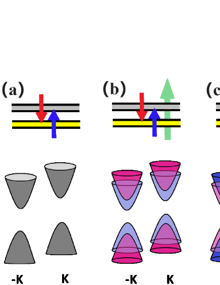
The proposal for electric-filed tuned AVHE in AFM monolayer is schematically illustrated in Figure 1. We consider a hexagonal centrosymmetric monolayer with two-layer magnetic atoms with intralayer FM and interlayer AFM orderings (A-type AFM ordering), which possesses energy extrema of conduction or valance bands located at high symmetry -K and K points. The lattice of our proposed system has inversion symmetry, but the opposite spin vectors of the two sublattices break spatial inversion () symmetry and time reversal () symmetry, which produces spontaneous valley polarization (Figure 1 (a)). However, the the spin degeneracy of -K and K valleys is maintained due to symmetry, which prohibits the AVHE in AFM monolayer.
There is zero berry curvature () everywhere in the momentum space due to symmetry. However, layer-locked hidden Berry curvature can appear, because each layer breaks the symmetry. Due to layer-spin locking, the Berry curvatures for the spin-up and spin-down channels are equal in magnitude and opposite in sign. The layer-locked hidden Berry curvature can give rise to layer-Hall effect.
Here, an out-of-plane electric field is applied to break the symmetry, which can remove spin degeneracy of -K and K valleys. The out-of-plane electric field can produce layer-dependent electrostatic potential ( and denote the electron charge and the layer distance.), which induces spin splitting effect. With breaking symmetry, the spin splitting at the -K and K valleys can be realized (Figure 1 (b)), resulting in the AVHE. Moreover, it is expected that the spin order at both the -K and K valleys can be reversed through manipulating the direction of out-of-plane electric field (Figure 1 (c)).
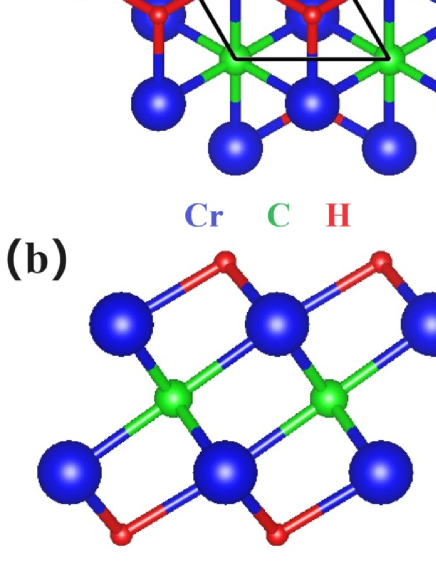
The H-functionalized MXene ()v15 can be used as a real material to verify our proposal. The is a half-metallic ferromagnet, which has been successfully synthesized in experimentv16 . By surface functionalization with H in , a ferromagnetic-antiferromagnetic transition and a metal-insulator transition can be induced simultaneouslyv15 . In addition to this, possesses A-type AFM ordering with energy extrema of valance bands located at -K and K points, which meets the requirements of our proposal.
III Computational detail
Within density functional theory (DFT)1 , the spin-polarized first-principles calculations are carried out within the projector augmented-wave (PAW) method, as implemented in Vienna ab initio Simulation Package (VASP)pv1 ; pv2 ; pv3 . The generalized gradient approximation of Perdew-Burke-Ernzerhof (PBE-GGA)pbe as the exchange-correlation functional is adopted. The kinetic energy cutoff of 500 eV, total energy convergence criterion of eV, and force convergence criterion of 0.0001 are set to obtain the accurate results. To account for the localized nature of Cr-3 orbitals, a Hubbard correction =3.0 eVv13 ; v13-1 is used by the rotationally invariant approach proposed by Dudarev et al. The SOC is incorporated for investigation of valley splitting and magnetic anisotropy energy (MAE). The vacuum space of more than 20 along direction is introduced to avoid interactions between neighboring slabs. A 21211 Monkhorst-Pack k-point meshes are used to sample the Brillouin zone (BZ) for calculating electronic structures. Based on finite displacement method, the interatomic force constants (IFCs) are calculated by employing 551 supercell with AFM ordering, and the phonon dispersion spectrum is obtained by the Phonopy codepv5 . The Berry curvatures are calculated directly from the calculated wave functions based on Fukui’s methodbm , as implemented in the VASPBERRY codebm1 ; bm2 .
IV Crystal and electronic structures
It has been proved that monolayer possesses A-type AFM ordering with dynamical, mechanical, and thermal stabilitiesv15 . The crystal structures of along with the first BZ are shown in Figure 2 (a), (b) and (c), which crystallizes in the space group (No.164), hosting inversion symmetry. It consists of five atomic layers in the sequence of H-Cr-C-Cr-H, and the magnetic Cr atoms distribute in two layers. The optimized equilibrium lattice constants are ==2.99 by GGA+ method, which agrees well with previous result(2.95 v15 ). Based on its energy band structures in FIG.S1 of electronic supplementary information (ESI) or in ref.v15 , the valence band maximum (VBM) of is at point, not -K or K point. To clearly clarify our proposal, the biaxial strain (=0.96) is applied to change VBM of from to -K or K point. To determine magnetic ground state of , the FM and three AFM configurations (AFM1, AFM2 and AFM3) are constructed, as shown in FIG.S2 of ESI, and the AFM1 is called A-type AFM state. Calculated results show that the energy of AFM1 per unit cell is 281 meV, 50 meV and 399 meV lower than those of FM, AFM2 and AFM3 cases by GGA+, confirming that the strained still possesses AFM1 ground state. The calculated phonon spectrum of strained with no obvious imaginary frequencies is shown in Figure 2 (d), indicating its dynamic stability.
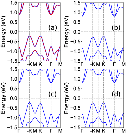
The energy band structures of by using both GGA and GGA+SOC are plotted in Figure 3. According to Figure 3 (a), no spin splitting can be observed due to the symmetry, and is an indirect band gap semiconductor. The energies of -K and K valleys in the valence band are degenerate. Figure 3 (b) shows that the valley polarization can be induced by SOC, and the valley splitting is 49 meV. The energy of K valley is higher than one of -K valley, and the valley polarization can be switched, when the magnetization direction is reversed (Figure 3 (c)). When the magnetization direction of is in-plane along direction (Figure 3 (d)), no valley polarization can be observed. Therefore, the magnetic orientation is determined by MAE, which can be obtained by , where and mean that spins lie in the plane and out-of-plane. The calculated MAE is 27/unit cell, indicating the out-of-plane easy magnetization axis of . This confirms the realization of our proposed design principles. The total magnetic moment of per unit cell is strictly 0.00 with magnetic moment of bottom/top Cr atom being 3.09 /-3.09 . When the SOC is included, the spin degeneracy is still maintained for both out-of-plane and in-plane magnetization directions.
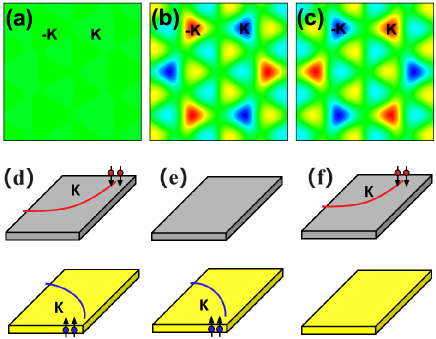
For , the distribution of Berry curvatures of total, spin-up and spin-down are plotted in Figure 4. It is observed that total berry curvature everywhere in the momentum space is zero due to symmetry. The extremes of spin-resolved Berry curvatures locate at the -K and K valleys, which have opposite signs for the same spin channel. For the same valley at different spin channel, the Berry curvatures are also opposite. When a longitudinal in-plane electric field is applied, the Bloch carriers will acquire an anomalous transverse velocity v17 . By shifting the Fermi level between the -K and K valleys in the valence band, the spin-up and spin-down holes from K valley will accumulate along opposite sides of different layer under a longitudinal in-plane electric field, resulting in the valley layer-spin Hall effect (Figure 4 (d)), but the AVHE is absent.
V electric field induces spin splitting
To induce spin splitting in , symmetry should be broken. Here, an out-of-plane electric field (0.00-0.10 ) is applied, which can break symmetry, and lift spin degeneracy of valleys. The generates exactly the same results except spin orders since two Cr layers are related by a glide mirror symmetry, but have opposite magnetic moments. Firstly, the magnetic ground state under out-of-plane electric field is determined by the energy difference between FM/AFM2/AFM3 and AFM1 configurations. Within considered range, based on FIG.S3 of ESI, the AFM1 ordering is always ground state. The MAE vs is plotted in FIG.S4, and the positive MAE confirms that the easy axis of is out-of-plane direction within considered range. These ensure that our design principles can be realized in .
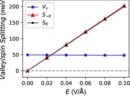
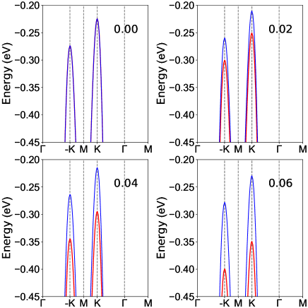
The energy band structures of at representative by using GGA+SOC are plotted in FIG.S5 of ESI, and the enlarged figures of spin-resolved energy band structures near the Fermi level for the valence band are shown in Figure 5. For valence band, the valley splitting and spin splitting at -K and K valleys as a function of are plotted in Figure 6. The spontaneous valley polarization of about 49 meV is maintained within considered range. When electric filed is applied, it is clearly seen that there is spin splitting, which is due to layer-dependent electrostatic potential caused by out-of-plane electric field. Spin splitting and electric field strength show a linear relationship. In fact, the spin splitting can be approximately calculated by . Taking =0.02 as a example, the of is 2.37 A, and the estimated spin splitting is approximately 47 meV, which is close to the first-principle result 41 meV. The coexistence of spin splitting and valley polarization is essential for the realization of AVHE. When the electric filed changes from to , the layer-dependent electrostatic potential is also reversed. The sizes of spin splitting and valley splitting remain unchanged, but the spin order of spin splitting reversed (FIG.S6 of ESI), which is consistent with our proposed design principle.
For at =0.02, the distribution of Berry curvatures of spin-up and spin-down are shown in FIG.S7. It is clearly seen that the Berry curvatures are opposite for the same valley at different spin channel and different valley at the same spin channel. By shifting the Fermi level between the -K and K valleys in the valence band, only the spin-up holes from the K valley move to the bottom boundary of the sample under an in-plane electric field (Figure 4 (e)), producing layer-locked AVHE. Conversely, by reversing the electric field direction, the spin-down holes from the K valley will move to the top opposite side of the sample by proper hole doping (Figure 4 (f)). This accumulation of spin-polarized holes produces a net charge/spin current, and Figure 4 (e) and Figure 4 (f) generate opposite voltage.
VI Conclusion
In summary, we present a model to induce AVHE in A-type hexagonal AFM monolayer by applying electric filed. The validity of our proposal is confirmed by an extensive study of within the first-principles calculations. The spontaneous valley polarization can occur in , but the spin splitting of -K and K valleys is absent. The introduction of an out-of-plane electric field results in spin splitting due to layer-dependent electrostatic potential. The layer-locked hidden Berry curvature produces layer-locked AVHE. Our works enriches the AVHE in AFM monolayers, and provide great potential for developing energy-efficient and ultrafast valleytronic devices.
Acknowledgements.
This work is supported by Natural Science Basis Research Plan in Shaanxi Province of China (2021JM-456). We are grateful to Shanxi Supercomputing Center of China, and the calculations were performed on TianHe-2.References
- (1) J. R. Schaibley, H. Yu, G. Clark, P. Rivera, J. S. Ross, K. L. Seyler, W. Yao and X. Xu, Nat. Rev. Mater. 1, 16055 (2016).
- (2) G. Pacchioni, Nat. Rev. Mater. 5, 480 (2020).
- (3) S. A. Vitale, D. Nezich, J. O. Varghese, P. Kim, N. Gedik, P. Jarillo-Herrero, D. Xiao and M. Rothschild, Small 14, 1801483 (2018).
- (4) D. Xiao, M. C. Chang and Q. Niu, Rev. Mod. Phys. 82, 1959 (2010).
- (5) A. Srivastava, M. Sidler, A. V. Allain, D. S. Lembke, A. Kis and A. Imamoglu, Nat. Phys. 11, 141 (2015).
- (6) K. F. Mak, K. He, J. Shan and T. F. Heinz, Nat. Nanotechnol. 7, 494 (2012).
- (7) H. Zeng, J. Dai, W. Yao, D. Xiao, and X. Cui, Nat. Nanotechnol. 7, 490 (2012).
- (8) M. Zeng, Y. Xiao, J. Liu, K. Yang and L. Fu, Chem. Rev. 118, 6236 (2018).
- (9) C. Zhao, T. Norden, P. Zhang, P. Zhao, Y. Cheng, F. Sun, J. P. Parry, P. Taheri, J. Wang, Y. Yang, T. Scrace, K. Kang, S. Yang, G. Miao, R. Sabirianov, G. Kioseoglou, W. Huang, A. Petrou and H. Zeng, Nat. Nanotechnol. 12, 757 (2017).
- (10) D. MacNeill, C. Heikes, K. F. Mak, Z. Anderson, A. Kormnyos, V. Zlyomi, J. Park and D. C. Ralph, Phys. Rev. Lett. 114, 037401 (2015).
- (11) X. X. Zhang, Y. Lai, E. Dohner, S. Moon, T. Taniguchi, K. Watanabe, D. Smirnov and T. F. Heinz, Phys. Rev. Lett. 122, 127401 (2019).
- (12) D. MacNeill, C. Heikes, K. F. Mak, Z. Anderson, A. Korm nyos, V. Zlyomi, J. Park and D. C. Ralph, Phys. Rev. Lett. 114, 037401 (2015).
- (13) L. Xu, M. Yang, L. Shen, J. Zhou, T. Zhu and Y. P. Feng, Phys. Rev. B 97, 041405 (2018).
- (14) C. Zhao, T. Norden, P. Zhang, P. Zhao, Y. Cheng, F. Sun, J. P. Parry, P. Taheri, J. Wang, Y. Yang, T. Scrace, K. Kang, S. Yang, G. Miao, R. Sabirianov, G. Kioseoglou, W. Huang, A. Petrou and H. Zeng, Nat. Nanotechnol. 12, 757 (2017).
- (15) W. Zhou, Z. Yang, A. Li, M. Long and F. Ouyang, Phys. Rev. B 101, 045113 (2020).
- (16) T. Cao, G. Wang, W. Han, H. Ye, C. Zhu, J. Shi, Q. Niu, P. Tan, E. Wang, B. Liu and J. Feng, Nat. Commun. 3, 887 (2012).
- (17) L. Xie and X. Cui, Proc. Natl. Acad. Sci. USA 113, 3746 (2016).
- (18) W. Y. Tong, S. J. Gong, X. Wan and C. G. Duan, Nat. Commun. 7, 13612 (2016).
- (19) Y. B. Liu, T. Zhang, K. Y. Dou, W. H. Du, R. Peng, Y. Dai, B. B. Huang, and Y. D. Ma, J. Phys. Chem. Lett. 12, 8341 (2021).
- (20) Z. Song, X. Sun, J. Zheng, F. Pan, Y. Hou, M.-H. Yung, J. Yang, and J. Lu, Nanoscale 10, 13986 (2018).
- (21) J. Zhou, Y. P. Feng, and L. Shen, Phys. Rev. B 102, 180407(R) (2020).
- (22) P. Zhao, Y. Ma, C. Lei, H. Wang, B. Huang, and Y. Dai, Appl. Phys. Lett. 115, 261605 (2019).
- (23) X. Y. Feng, X. L. Xu, Z. L. He, R. Peng, Y. Dai, B. B. Huang and Y. D. Ma, Phys. Rev. B 104, 075421 (2021)
- (24) Y. Zang, Y. Ma, R. Peng, H. Wang, B. Huang, and Y. Dai, Nano Res. 14, 834 (2021).
- (25) R. Peng, Y. Ma, X. Xu, Z. He, B. Huang, and Y. Dai, Phys. Rev. B 102, 035412 (2020).
- (26) W. Du, Y. Ma, R. Peng, H. Wang, B. Huang, and Y. Dai, J. Mater. Chem. C 8, 13220 (2020).
- (27) R. Li, J. W. Jiang, W. B. Mi and H. L. Bai, Nanoscale 13, 14807 (2021).
- (28) T. Jungwirth, J. Sinova, A. Manchon, X. Marti, J. Wunderlich, and C. Felser, Nat. Phys. 14, 200 (2018).
- (29) T. Zhao, S. Xing, J. Zhou, N. Miao and Z. Sun, Journal of Materiomics (2023), doi: https://doi.org/10.1016/j.jmat.2023.10.008.
- (30) W. Du, R. Peng, Z. He, Y. Dai, B. Huang, and Y. Ma, npj 2D Mater. Appl. 6, 11 (2022).
- (31) Y. Xu, H. Liu, Y. Dai, B. Huang and W. Wei, Appl. Phys. Lett. 122, 242404 (2023).
- (32) P. Hohenberg and W. Kohn, Phys. Rev. 136, B864 (1964); W. Kohn and L. J. Sham, Phys. Rev. 140, A1133 (1965).
- (33) G. Kresse, J. Non-Cryst. Solids 193, 222 (1995).
- (34) G. Kresse and J. Furthmller, Comput. Mater. Sci. 6, 15 (1996).
- (35) G. Kresse and D. Joubert, Phys. Rev. B 59, 1758 (1999).
- (36) J. P. Perdew, K. Burke and M. Ernzerhof, Phys. Rev. Lett. 77, 3865 (1996).
- (37) J. He, G. Ding, C. Zhong, S. Li, D. Li and G. Zhang, Nanoscale, 11, 356 (2018).
- (38) A. Togo, F. Oba and I. Tanaka, Phys. Rev. B 78, 134106 (2008).
- (39) T. Fukui, Y. Hatsugai and H. Suzuki, J. Phys. Soc. Japan. 74, 1674 (2005).
- (40) H. J. Kim, https://github.com/Infant83/VASPBERRY, (2018).
- (41) H. J. Kim, C. Li, J. Feng, J.-H. Cho, and Z. Zhang, Phys. Rev. B 93, 041404(R) (2016).
- (42) C. Si, J. Zhou and Z. Sun, ACS Appl. Mater. Interfaces 7, 17510 (2015).
- (43) B. Soundiraraju, R. Raghavan and B.K. George, ACS Appl. Nano Mater. 3, 11007 (2020).
- (44) D. Xiao, M. C. Chang and Q. Niu, Rev. Mod. Phys. 82, 1959 (2010).