Spin-polarized nearly-free electron channels on the Ca2N electrenes
Abstract
ABSTRACT
Two-dimensional (2D) materials combined with the presence of surface nearly-free electrons (NFE) have been considered quite interesting platforms to be exploited for the development of 2D electronic devices. Further incorporation of foreign elements adds a new degree of freedom to engineer the electronic as well as the magnetic properties of 2D materials. Here we have performed an ab-initio study of Ca2N electrenes fully (i.e., both sides) adsorbed by hydrogen (H/Ca2N/H) and fluorine (F/Ca2N/F) atoms. The NFE states are suppressed in these systems, followed by the appearance of a net magnetic moment localized in the nitrogen atoms intercalated by the hydrogenated or fluorinated calcium layers. In the sequence, we have proposed lateral heterostructures combining the H/Ca2N/H or F/Ca2N/F regions with pristine Ca2N electrenes [(Ca2N)(X/Ca2N/X), with X = H or F]. We found that the magnetic moment of the hydrogenated or fluorinated regions promotes the emergence of spin-polarized NFE states confined along the pristine (Ca2N) stripes. Further electronic transport calculations reveal that the (X/Ca2N/X) regions act as spin-dependent scattering centers, spin-filters. We believe that these findings make an important contribution to the development of spintronic devices based on 2D electrides.
I Introduction
Electrides are a class of ionic crystals in which there are excess valence electrons that behave as anions and don’t belong in an atomic orbital 1; 2; 3. There are some electrides that crystallize in a layered structure and these anionic electrons are located in the interlayer gap forming a 2D electron gas. As a consequence, these materials offer properties such as low work functions, high electrical conductivity, and rich surface chemistries 4. The layered structure of electrides permits the synthesis of 2D electrides by an exfoliation process, once that interlayers bonding is van der Waals (vdW) 5. The electride monolayer, often referred as electrene, has been experimentally obtained with electride samples of Ca2N and Y2C. In these samples, nearly free electrons (NFE) are situated on both sides of the monolayer 6; 7.
Some studies show that electrides are interesting materials that can have different physical properties and applications such as topological phases8; 9; 10; 11; 12; 13; 14, great potential as an anode to batteries 15; 16; 17, metal-semiconductor transition under pressure18 and doping effects on vdW heterostructures with graphene 19; 20.
The presence of anionic electrons located on both sides of electrenes makes the surface be reactive. Furthermore, the structure resembling MXenes facilitates the functionalization process, potentially leading to varied electronic and magnetic properties compared to the pristine structure21. Recently, we have shown that the full oxidation on one side of monolayer Ca2N and both sides of bilayer Ca2N induce a structural transition from hexagonal to tetragonal, followed by the emergence of half-metallic channels, near the Fermi level, shielded from the environment conditions by the CaO (cover) layers22. Moreover, the Ca2N functionalization via Hydrogen (H) induces a metalic-semiconductor transition when the H is adsorbed on one side of the Ca2N surface, and when H is adsorbed on both sides of the surface the functionalized Ca2N becomes a half-metal 23. In addition, the process of functionalization enables some applications of the electrenes, such as in batteries through adsorption of hydroxyl 24.
The design of heterostructures, guided by a strategic combination of materials with suitable properties, has been the subject of intense research addressing the development of electronic devices that meet the current demand. Such a combination can be done, in most cases, by vertical or lateral (in-plane) stacking of different materials like WS2/MoS225; 26 or graphene/boron-nitride27. In particular, lateral heterostructures based on 2D platforms can also be realized by combining distinct structural phases of the same material28; 29 or through the selective incorporation (adsorption) of foreign elements, giving rise nanoroads with magnetic properties in graphene oxide, and diamane oxide films30; 31.
In this work, we performed an ab-initio study of the energetic stability and electronic properties of fully hydrogenated (H/Ca2N/H) and fluorinated (F/Ca2N/F) electrenes. We found that both systems are characterized by (i) the suppression of the NFE states on the Ca2N surface, and (ii) the a net magnetic moment localized in the nitrogen atoms. In the sequence, we focused on the lateral heterostructures composed by a combination of H/Ca2N/H or F/Ca2N/F regions (or stripes) separated by pristine Ca2N stripes [(Ca2N)(X/Ca2N/X), with X = H or F]. Our findings reveal the emergence of channels of spin-polarized NFE surface states on the pristine Ca2N regions, which are induced by the X/Ca2N/X regions. Further electronic transport calculations show that the electron scattering rate is spin-dependent in the (X/Ca2N/X) regions, thus acting as a spin-filters.
II Computational details
The calculations were performed by using the density functional theory (DFT)32, as implemented in the Vienna Ab initio Simulation Package (VASP)33; 34. The exchange-correlation functional was considered the gradient generalized approximation of Perdew-Burke-Ernzerhof (GGA-PBE)35. The atomic positions of the primitive hexagonal cell of Ca2N, H/Ca2N/H, and F/Ca2N/F were relaxed until the residual forces were converged to within 5 meV/Å and the structural relaxation (variable-cell) was performed within a pressure convergence of 0.05 Kbar with a Brillouin zone sampling of the 881 k-point mesh36. In the lateral heterostructures we used supercells with a vacuum region of 10 Å and considered an energy cutoff of 500 eV for the plane wave basis set. The Brillouin zone was sampled using a 691 and 961 k-point mesh36, for zigzag and armchair directions, respectively, and more structural supercell details are described throughout the text.
The electronic transmission probability (T) was calculated within the non-equilibrium Green’s Functions (NEGF) formalism using the DFT Hamiltonian and implemented in the Siesta and TranSiesta codes37; 38. The Kohn-Sham orbitals were expanded in a linear combination of numerical pseudo-atomic orbitals, using a single-zeta basis set including polarization functions39. The BZ samplings were performed using two different sets of k-point meshes, 120300 according to the electronic transport directions. The total transmission probability of electrons with energy and bias voltage , , from the left electrode to reach the right electrode passing through the scattering region is given by,
where is the coupling with the left and right electrodes and is the retarded (advanced) Green function matrix of the scattering region.
III Results and Discussions
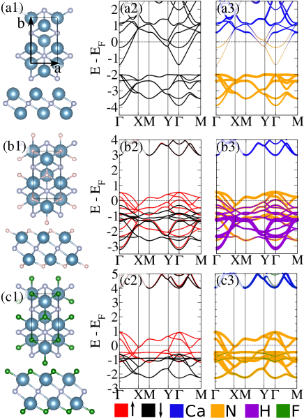
In Fig. 1(a1) we show the structural model and the electronic band structure of pristine Ca2N monolayer (ML). We have considered a tetragonal unit-cell with (equilibrium) lattice vectors of = 3.55 Å, and = 6.17 Å . The electronic band structure, Figs. 1(a2) and (a3), is characterized by (i) the formation of parabolic metallic bands at the point, a signature of the emergence of NFE on the ML surface, and (ii) a set of fully occupied energy bands, between 2 and 4 eV below the Fermi level (), attributed to the N- orbitals.
III.1 Hydrogenation and Fluorination
A promising method to regulate or fine-tune the mechanical and electrical features of 2D systems is hydrogenation or fluorination. In the case of graphene as the 2D platform, semiconductor systems are produced by the complete adsorption of H or F atoms, resulting in graphane or fluorgraphene40.
In Figs. 1(b1) and (c1) we present the lowest energy geometries of the fully hydrogenated and fluorinated Ca2N ML (hereinafter labeled as H/Ca2N/H and F/Ca2N/F), which are characterized by the (H/F) adatoms aligned with the Ca atoms at the opposite side of the ML23. Our results of the equilibrium lattice constants ( and ), see Table 1, reveal that the Ca2N ML lattice is slightly shrinked by about 2 %. The formation energy () and binding energy () of X/Ca2N/X (with X = H or F) is defined as the total energy difference between the final system and the sum of the total energies of the separated components, Ca2N ML and X2 molecule, and X atom, respectively. Negative values indicate exothermic processes. Our result of for H/Ca2N/H agrees with that obtained by Qiu et al.23. On the other hand, it is worth noting that in we are comparing the final system, X/Ca2N/X, with respect to the energetically stable molecular systems, X2. Thus, our results of allow us to infer that F/Ca2N/F is substantially more stable than H/Ca2N/H. Indeed, a similar stability picture has been predicted in graphene, i.e. graphane versus fluorgraphene40.
| Ca2N-H | 3.50 | 6.06 | ||
| Ca2N-F | 3.48 | 6.03 |
Upon the formation of Ca-H or Ca-F chemical bonds, we find that (i) the anionic electrons on the Ca2N surface has been suppressed, as well as the NFE parabolic bands crossing the Fermi level, as depicted in Figs. 1(b2)-(b3) and (c2)-(c3); followed by (ii) an increase of the work function () from 3.6 eV (pristine Ca2N ML) to 5.44 and 5.91 eV in H/Ca2N/H and F/Ca2N/F respectively; and (iii) the emergence of a net magnetic moment of 0.63 /N. In both systems, the magnetization is dictated by the unpaired states near the Fermi level, resulting in half-metallic systems mediated by the planar N- orbitals. At the ground state configuration, X/Ca2N/X presents a ferromagnetic (FM) phase, which is in agreement with Qiu et al., and characterized by an energy gain, , of and meV/unit-cell, for X = H and F, respectively. In Ref. 23, the authors obtained of meV/unit-cell in H/Ca2N/H.
III.2 Lateral Heterostructures
A promising route for creating electronic (nano)devices is the construction of 1D structures at the atomic level on 2D platforms. For instance, the creation of nanodots and linear stripes on graphene as a result of the recent manipulation of hydrogen adatoms has produced 0D and 1D electronic confinement phenomena.41 It is worth noting that, more than ten years ago, several works have already predicted such electronic confinement and the emergence of magnetism in 1D nanostructures on graphane42; 43; 44, and more recently on graphene oxide30.
As discussed above, the pristine Ca2N ML is non-magnetic and has NFE states localized on the surface. In contrast, H/Ca2N/H and F/Ca2N/F are characterized by the emergence of magnetic moment localized on the nitrogen atoms, resulting in half-metallic states. In view of these results, in the sequence, we investigated the electronic and magnetic properties of the (Ca2N)(X/Ca2N/X) lateral heterostructures, characterized by pristine Ca2N ML intercalated by periodic stripes of hydrogenated or fluorinated regions, (Ca2N)(X/Ca2N/X)n, with =3, 4, and 5.
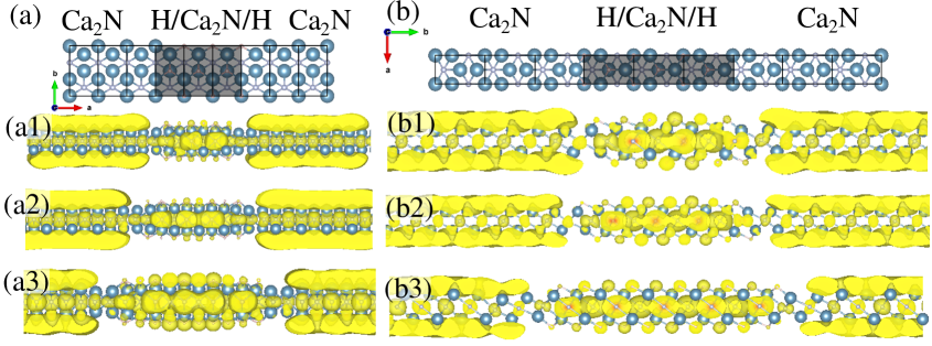
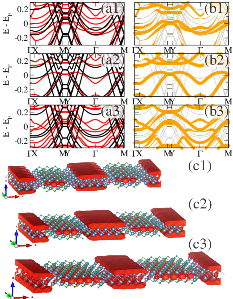
We have studied (Ca2N)(X/Ca2N/X)n heterostructures composed by six unit cells of Ca2N, namely (Ca2N)6(X/Ca2N/X)n, forming armchair (ARM) [Fig. 2(a)] and zigzag (ZZ) [Fig. 2(b)] interfaces between the (Ca2N)6 and (X/Ca2N/X)3 stripes. We found that the electronic states close to the Fermi level, eV, are predominantly localized on the (i) nitrogen atoms intercalated by hydrogenated/fluorinated calcium layers and (ii) on the surface of the non-hydrogenated Ca2N regions, as depicted in Figs. 2(a1)-(a3) and (b1)-(b3) for X = H. These findings suggest the emergence of NFE surface states propagating along the (Ca2N)6 stripes, confined by the hydrogenated (H/Ca2N/H)n walls. Similar results were obtained in the fluorinated heterostructures, (Ca2N)6(F/Ca2N/F)n.
Total energy comparisons between the ARM and ZZ interfaces, , reveal an energetic preference for the ARM interface, Table 2. As expected, the role played by the orientation of the edge interface becomes less important as the hydrogenated or fluorinated region increases, i.e. for larger values of .
| (Ca2N)6(X/Ca2N/X)n | |
|---|---|
| (Ca2N)6(H/Ca2N/H)3 | -0.144 eV/H |
| (Ca2N)6(H/Ca2N/H)4 | -0.101 eV/H |
| (Ca2N)6(H/Ca2N/H)5 | -0.073 eV/H |
| (Ca2N)6(F/Ca2N/F)3 | -0.136 eV/F |
| (Ca2N)6(F/Ca2N/F)4 | -0.103 eV/F |
| (Ca2N)6(F/Ca2N/F)5 | -0.069 eV/F |
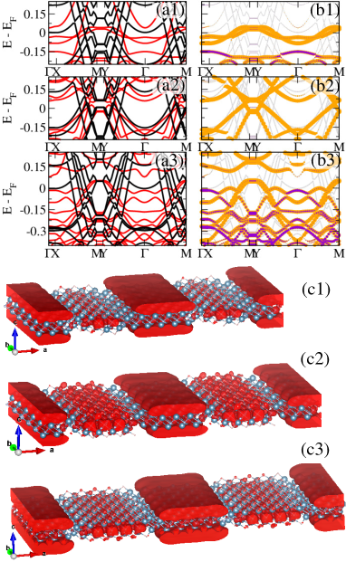
In the sequence, we will focus on the electronic properties of the armchair (Ca2N)6/(H/Ca2N/H)n heterostructures. The presence of a net magnetic moment of the nitrogen atoms sandwiched by the hydrogenated Ca layers, H/Ca2N/H, leads to the formation of spin-polarized bands, indicated by the red (spin-up) and black (spin-down) solid lines in Figs. 3(a1)-(a3), for = 3, 4, and 5. Indeed, further orbital projected electronic band structure on the hydrogenated region [Fig. 3(b1)-(b3)] reveals that the spin-up N- orbitals bring an important contribution to the spin-polarized states near the Fermi level. It is noticeable the predominance of spin-up metallic bands for wave-vectors parallel (Y- and X-M directions) and quasi-parallel (-M direction) to the (Ca2N)6/(H/Ca2N/H)n stripes. Meanwhile, along the -X and Y-M directions, the electronic states are characterized by dispersionless energy bands resulting from the electronic confinement perpendicularly to the stripes. Further spin-density distributions, , depicted in Figs. 3(c1)-(c3), confirm the formation of 1D spin-polarized NFE states spreading out on the (Ca2N)6 surface confined by (H/Ca2N/H)n. We found similar results in the fluorinated systems, (Ca2N)6(F/Ca2N/F)n, Fig. 5 in the appendix. Those findings suggest the emergence of spin-polarized electronic transport channels based on the NFE along the Ca2N confined by hydrogenated or fluorinated stripes.
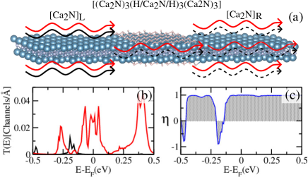
On the other hand, it is expected that the NFE states are no longer spin-polarized far from the hydrogenated or fluorinated stripes, so it is worth examining the role played by the hydrogenated stripes in the scattering process of the non-spin-polarized NFE states. In this case, as a test of concept, we have considered non-spin-polarized (pristine) Ca2N leads connected to the (Ca2N)3(H/Ca2N/H)3(Ca2N)3 lateral heterostructure,
[Ca2N]–(Ca2N)3/(H/Ca2N/H)3/Ca2N)3–[Ca2N].
[Ca2N] and [Ca2N] indicate the left and right leads, respectively, as schematically shown in Fig. 4(a). Our results of the transmittance, , close to the Fermi level [Fig. 4(b)] demonstrates the dominance of the spin-up transmission channels [], leading to a net spin-polarized current [Fig. 4(b)]. Such a spin-anisotropy [] in the electronic transport properties can be measured as,
Our results of , presented in Fig. 4(c), show the emergence of a nearly full spin-up current [] at the limit of low bias voltage, eV; followed by a contribution of upon further increase of the bias voltage, due to the presence of spin-down channels for eV. Such dominance of spin-up transmittance can be attributed to (i) the spin polarization of the (Ca2N)(H/Ca2N/H)(Ca2N) contact region, and (ii) the number (density of states) of spin-up channels within the energy interval close to the Fermi level, eV, Fig. 3(a1). Similar results, regarding the spin-polarized currents, are expected for other (X/Ca2N/X)n widths () with X = H, and F. We believe that these findings are important for the development and design of spintronic devices in 2D materials, in particular, the ones based on the hydrogenation or fluorination Ca2N electrenes.
IV Summary and Conclusions
In summary, we have performed a first-principles investigation of the electronic properties of the hydrogenated and fluorinated Ca2N electrenes, X/Ca2N/X, with X = H and F. A net magnetic moment arises as a result of the partial occupation of the nitrogen atoms between the passivated Ca atoms, followed by the suppression of the NFE states on the Ca2N surface upon such passivation. In the sequence, we have considered lateral heterostructures composed of a combination of pristine and passivated Ca2N MLs, (Ca2N)(X/Ca2N/X). Those heterostructures are characterized by the emergence of 1D channels of spin-polarized NFE states on the (Ca2N) surface confined by the passivated (X/Ca2N/X) stripes. Moreover, we found that the passivated X/Ca2N/X regions act as a spin-dependent scattering center, giving rise to spin-polarized electronic current. These findings show that the passivation of Ca2N electrenes is an appealing route to designing spin-polarized electronic devices based on NFEs on 2D platforms.
Acknowledgements.
The authors acknowledge financial support from the Brazilian agencies CNPq, CAPES, and FAPEMIG, INCT-Nanomateriais de Carbono, Rede-Mineira de Materiais 2D, and the CENAPAD-SP and Laboratório Nacional de Computação Científica (LNCC-SCAFMat2) for computer time.V Appendix
In Figure 5 we show the electronic band structure and the respective orbital projected electronic band structure of the (Ca2N)6/(F/Ca2N/F)3 (a1)-(b1), (Ca2N)6/(F/Ca2N/F)4 (a2)-(b2), and (Ca2N)6/(F/Ca2N/F)5 (a3)-(b3). In Figure 5(c1)-(c3), we present the spin-density distribution of (Ca2N)6/(F/Ca2N/F)n.
References
- Oh et al. (2016) J. S. Oh, C.-J. Kang, Y. J. Kim, S. Sinn, M. Han, Y. J. Chang, B.-G. Park, S. W. Kim, B. I. Min, H.-D. Kim, et al., Journal of the American Chemical Society 138, 2496 (2016).
- Sui et al. (2019) X. Sui, J. Wang, and W. Duan, The Journal of Physical Chemistry C 123, 5003 (2019).
- Lee et al. (2013) K. Lee, S. W. Kim, Y. Toda, S. Matsuishi, and H. Hosono, Nature 494, 336 (2013).
- Druffel et al. (2017) D. L. Druffel, A. H. Woomer, K. L. Kuntz, J. T. Pawlik, and S. C. Warren, Journal of Materials Chemistry C 5, 11196 (2017).
- Wang et al. (2018) J. Wang, L. Li, Z. Shen, P. Guo, M. Li, B. Zhao, L. Fang, and L. Yang, Materials 11, 2462 (2018).
- Druffel et al. (2016) D. L. Druffel, K. L. Kuntz, A. H. Woomer, F. M. Alcorn, J. Hu, C. L. Donley, and S. C. Warren, Journal of the American Chemical Society 138, 16089 (2016).
- Dale and Johnson (2017) S. G. Dale and E. R. Johnson, Physical Chemistry Chemical Physics 19, 27343 (2017).
- Hirayama et al. (2018) M. Hirayama, S. Matsuishi, H. Hosono, and S. Murakami, Physical Review X 8, 031067 (2018).
- Huang et al. (2018) H. Huang, K.-H. Jin, S. Zhang, and F. Liu, Nano letters 18, 1972 (2018).
- Park et al. (2018) C. Park, S. W. Kim, and M. Yoon, Physical review letters 120, 026401 (2018).
- Zhu et al. (2019) S.-C. Zhu, L. Wang, J.-Y. Qu, J.-J. Wang, T. Frolov, X.-Q. Chen, and Q. Zhu, Physical Review Materials 3, 024205 (2019).
- Zhang et al. (2018) X. Zhang, R. Guo, L. Jin, X. Dai, and G. Liu, Journal of Materials Chemistry C 6, 575 (2018).
- Zhang et al. (2019) X. Zhang, B. Fu, L. Jin, X. Dai, G. Liu, and Y. Yao, The Journal of Physical Chemistry C 123, 25871 (2019).
- Liu et al. (2019) L. Liu, C. Wang, S. Yi, D. K. Kim, C. H. Park, and J.-H. Cho, Physical Review B 99, 220401 (2019).
- Hou et al. (2016) J. Hou, K. Tu, and Z. Chen, The Journal of Physical Chemistry C 120, 18473 (2016).
- Chen et al. (2017) G. Chen, Y. Bai, H. Li, Y. Li, Z. Wang, Q. Ni, L. Liu, F. Wu, Y. Yao, and C. Wu, ACS applied materials & interfaces 9, 6666 (2017).
- Kocabas et al. (2018) T. Kocabas, A. Ozden, I. Demiroglu, D. Çakır, and C. Sevik, The journal of physical chemistry letters 9, 4267 (2018).
- Tang et al. (2018) H. Tang, B. Wan, B. Gao, Y. Muraba, Q. Qin, B. Yan, P. Chen, Q. Hu, D. Zhang, L. Wu, et al., Advanced Science 5, 1800666 (2018).
- Inoshita et al. (2017) T. Inoshita, M. Tsukada, S. Saito, and H. Hosono, Physical Review B 96, 245303 (2017).
- Choi et al. (2021) C.-G. Choi, J. Kim, H.-K. Choi, J. Cha, and S. Hong, Current Applied Physics 28, 13 (2021).
- Wu and Yao (2020) C.-W. Wu and D.-X. Yao, Journal of Magnetism and Magnetic Materials 493, 165727 (2020).
- Souza et al. (2020) P. H. Souza, J. E. Padilha, and R. H. Miwa, The Journal of Physical Chemistry C 124, 14706 (2020).
- Qiu et al. (2019) X.-L. Qiu, J.-F. Zhang, Z.-Y. Lu, and K. Liu, The Journal of Physical Chemistry C 123, 24698 (2019).
- Wang et al. (2019) D. Wang, H. Li, L. Zhang, Z. Sun, D. Han, L. Niu, X. Zhong, X. Qu, and L. Yang, Applied Surface Science 478, 459 (2019).
- Gong et al. (2014) Y. Gong, J. Lin, X. Wang, G. Shi, S. Lei, Z. Lin, X. Zou, G. Ye, R. Vajtai, B. I. Yakobson, et al., Nature materials 13, 1135 (2014).
- Fang et al. (2018) X. Fang, Q. Tian, Y. Sheng, G. Yang, N. Lu, J. Wang, X. Zhang, Y. Zhang, X. Yan, and B. Hua, Superlattices and Microstructures 123, 323 (2018).
- Ci et al. (2010) L. Ci, L. Song, C. Jin, D. Jariwala, D. Wu, Y. Li, A. Srivastava, Z. Wang, K. Storr, L. Balicas, et al., Nature materials 9, 430 (2010).
- Liu et al. (2018) X. Liu, Z. Zhang, L. Wang, B. I. Yakobson, and M. C. Hersam, Nature materials 17, 783 (2018).
- Silvestre et al. (2019) G. Silvestre, W. L. Scopel, and R. Miwa, Nanoscale 11, 17894 (2019).
- Khabibrakhmanov and Sorokin (2022) A. I. Khabibrakhmanov and P. B. Sorokin, Nanoscale 14, 4131 (2022).
- Varlamova et al. (2022) L. A. Varlamova, S. V. Erohin, K. V. Larionov, and P. B. Sorokin, The Journal of Physical Chemistry Letters 13, 11383 (2022).
- Hohenberg and Kohn (1964) P. Hohenberg and W. Kohn, Physical review 136, B864 (1964).
- Kresse and Furthmüller (1996a) G. Kresse and J. Furthmüller, Computational materials science 6, 15 (1996a).
- Kresse and Furthmüller (1996b) G. Kresse and J. Furthmüller, Physical review B 54, 11169 (1996b).
- Perdew et al. (1996) J. P. Perdew, K. Burke, and M. Ernzerhof, Physical review letters 77, 3865 (1996).
- Monkhorst and Pack (1976) H. J. Monkhorst and J. D. Pack, Physical review B 13, 5188 (1976).
- Soler et al. (2002) J. M. Soler, E. Artacho, J. D. Gale, A. García, J. Junquera, P. Ordejón, and D. Sánchez-Portal, Journal of Physics: Condensed Matter 14, 2745 (2002).
- Brandbyge et al. (2002) M. Brandbyge, J.-L. Mozos, P. Ordejón, J. Taylor, and K. Stokbro, Physical Review B 65, 165401 (2002).
- Artacho (1999) D. Artacho, Phys. Status Solidi B 215, 809 (1999).
- Leenaerts et al. (2010) O. Leenaerts, H. Peelaers, A. Hernández-Nieves, B. Partoens, and F. Peeters, Physical Review B 82, 195436 (2010).
- Cortés-del Río et al. (2020) E. Cortés-del Río, P. Mallet, H. González-Herrero, J. L. Lado, J. Fernández-Rossier, J. M. Gómez-Rodríguez, J.-Y. Veuillen, and I. Brihuega, Advanced Materials 32, 2001119 (2020).
- Chernozatonskii et al. (2007) L. A. Chernozatonskii, P. B. Sorokin, and J. W. Brüning, Applied Physics Letters 91, 183103 (2007).
- Wu et al. (2009) M. Wu, X. Wu, Y. Gao, and X. C. Zeng, Applied Physics Letters 94, 223111 (2009).
- Singh and Yakobson (2009) A. K. Singh and B. I. Yakobson, Nano Letters 9, 1540 (2009).