197 \xpatchcmd
Characterization of Semiconducting Materials Using the Van der Pauw Method
Abstract
Semiconductors are currently an active topic of study due to the endless range of applications in electronic hardware and computer engineering. In this experiment, the material properties (i.e. resistivity , Hall coefficient , and mobility ) of a doped GaAs sheet is described by utilizing Hall Effect and the Van der Pauw method with varying temperature and magnetic field values . It is determined that the sample is an -type semiconductor using the sign of , which is measured to be , at and . Furthermore, the rate of change for the slope and is increasing along at the rate of , meaning the charge accumulation caused by the current and Lorentz force is quadratic in . It is also discovered that , and therefore the electron drift velocity is reduced proportionally at higher -values. This method provides a potential analogue in quantum scales with the Quantum Hall Effect and characterisation of quantum dots.
The Hall Effect, since its discovery in 1879 by Edwin Hall (1), has been a significant concept in electromagnetism, utilized in electronics development (2) and actively studied in quantum electrodynamics, notably the quantum Hall Effect (3). In addition, semiconducting materials and the Hall Effect are closely related, as semiconductors are widely used in computer architecture and engineering, such as processor hardware and thermal regulation of electrical components (2; 4). With the size of computers moving towards scales of the quantum domain (5; 6), the Hall Effect will be substantial in studying semiconductors in molecular sizes such as quantum dots (6; 7).
In this experiment, a GaAs sample’s material properties are characterized by measuring currents and voltages at different locations in the sample. Varying the sample temperature and applied magnetic field , the Van der Pauw (VdP) method is used to measure the following values and their , dependence: (i) resistivity , (ii) the Hall coefficient , (iii) the hole or electron concentration, and (iv) mobility . Additionally, the doping type of the semiconductor is determined by inspecting the sign of . It is found that at non-zero magnetic fields, decreases in magnitude and is directly proportional to , has a stronger dependence in than , change in in temperature is affected by magnetic field, and the particular GaAs sample used in the experiment is a -type semiconductor.
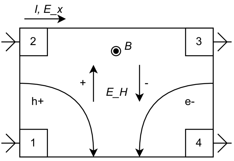
The conducting sheet itself has special properties that satisfies the necessary conditions for the use of the four-point probing scheme called the VdP method: thin, isotropic, and simply connected (8). This method is ideal since this method enables us to extract material information throughout all of the area of the sample, contrary to a unidirectional and one-dimensional measurement, and it also provides a way to isolate thermoelectric and contact offset contributions for the Hall voltage measurements (9). To obtain a value for resistivity , the current input (i.e. the current into contact and out of contact ) and voltage output for specific contact settings in Figure 1 is measured. Two trans-resistance measurements, denoted as for each, is used to calculate resistivity
| (1) |
where satisfies the VdP equation (8). The two trans-resistance measurements should be perpendicular to each other to get an average resistivity of the edges and therefore the average resistivity throughout the sample.
When a magnetic field is introduced to a conducting sheet in the direction shown in Fig. 1, the Lorentz force acts on the charge carried by the current perpendicular to its velocity, changing its trajectory to ultimately end on one of the sides. Thus, the magnetic field generates an induced electric field ( in Fig. 1), and therefore an associated potential difference (not shown). This production of an electric field perpendicular to the current in the sheet is called the Hall Effect (1) which is described by the equation
| (2) |
is the absolute value of the charge of an electron and is the charge carrier density, is the Hall voltage, the thickness of the sample, and are the current across the sample and the applied magnetic field respectively.
The Hall voltage is calculated using
| (3) |
where are the diagonal edges of the sample, and represent parallel and anti-parallel directions of the surface normal of the sheet and the magnetic field. The assumption here is that the voltage measurement is in the form of , where is a constant value. The subtraction is to eliminate voltage which is caused by the differing contact material. Substituting in Eq. 2 yields an equation that calculates with data obtained from VdP voltage measurements.
The mobility is a scalar factor that determines that determines the velocity of the charge carrier in terms of the electric field generated by the current.
| (4) |
It arises from Ohm’s law for surface currents , where is the conductivity of the sample, is the current density. In the -direction,
| (5) |
With the current density equation , resistivity-conductance relation , Eq. 2, and Eq. 4, the mobility is then obtained with
| (6) |
Its sign will determine the direction of the charge carrier (Fig. 1).
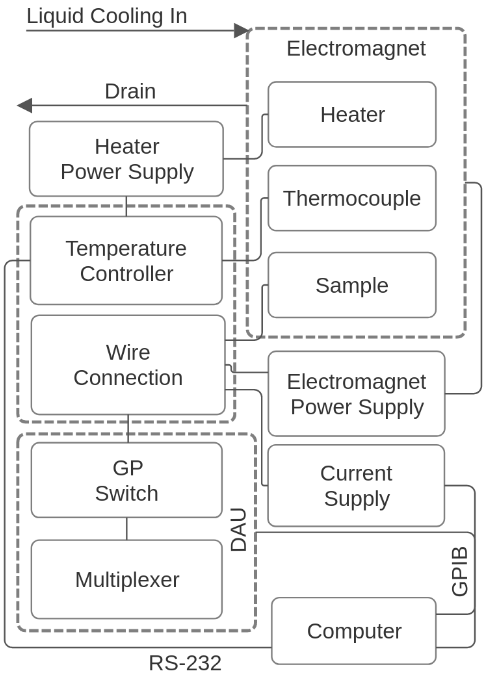
The general setup of the experiment is shown in Fig. 2. The sample is a 7 mm 7 mm GaAs sheet located in between two electromagnet coils with its strength adjusted by a power supply, with its corners coated with Ti/Pt/Au, connected to a lead (Fig. 1). The sample’s temperature is adjusted by a computer-controlled heater. The voltage and current measurement configurations are set automatically by a programmed general-purpose switch and a multiplexer. The reversal of the magnetic field (for use in Eq. 3) is done by turning the sample 180∘ from its initial orientation, such that the surface of the sample with the contacts are anti-parallel with the magnetic field.
All voltage and current data is taken for varying magnetic field () and temperature values. It may be limited due to the significant power drop of the heater at at this temperature but the range is ideal for the experiment, as it is within the operating temperature range for commercial semiconductors (10). The current supplied into the sample is a constant dc signal. For resistivity, each current-voltage pair , and , are measured simultaneously to obtain and respectively. These values are substituted to Eq. 1 to obtain . The errors may come from the approximation of in Eq. 1 and the random uncertainty coming from the trans-resistance measurements (Fig. 3). It is found that the input range of the measured trans-resistances is enough so that the relative error . Fig. 3(b) shows that the material resistivity has a high dependence in temperature, this makes the sheet susceptible to the generation of electromotive force due to spatial change in temperature called the Seebeck effect (11), which would create variability in the data taken. To mitigate, the material is “soaked” in the temperature for an arbitrary amount of time (20 seconds was chosen in our case) to allow for temperature distribution. This was done due to the time constraints. Ideally however, a reverse measurement of trans-resistances (i.e. and , same with voltages) would eliminate the errors from Seebeck effect.
The magnetic field may also have an offset when setting to very low values (e.g. ). At the lowest, the magnetic field is , this non-zero value may have come from other electrical components and/or resolution error. In the laboratory, there are wires in close proximity to the sample in which its arrangement may generate a very small magnetic field large enough that the magnetic field sensor reads a non-zero value. It cannot be the Earth’s magnetic field since at surface level, the strength of the magnetic field ranges from 0.25 - 0.65 Gs (12).
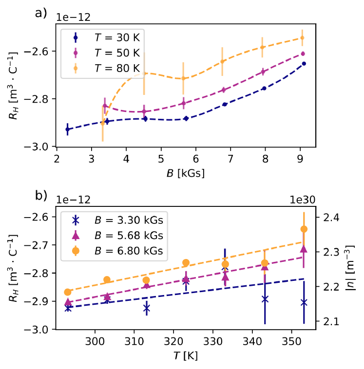
At and , we obtain . The sign of the Hall coefficient in Fig. 4 indicates that the sample is of an -type semiconductor. The calculations show that in general, a variation in leads to a trend towards which is expected with the form of Eq. 2. At lower -values (i.e. kGs) seems follow approach a finite value, which is reasonable as , , where a case of a finite value of then is possible at . This could be attributed to the random uncertainty of the magnetic field at lower values, leading to inaccurate measurements of which propagates to . Another reason could be due to the opposite carriers being present in the material in addition to the normal carriers at very low -values (13). Moreover, the change in and over increases along with (Fig. 4). For the temperature response of , its slope changes with with the rate . It confirms that increases faster than , as it is the only measured variable in Eq. 2, , , and are set values. To elaborate, it means that the linear increase of gives a quadratic increase in . Physically, the charge accumulation at the sides of the sample increases such that the ratio increases linearly.
To determine whether over is caused by a change in particle density or drift velocity (Fig. 4(b)), mobility has to be analysed. First, the and response of is calculated with Eq. 1, with the results shown in Fig. 3. The resistivity appears to have a stronger dependence to temperature compared to magnetic field. As such, it is expected that the mobility will also have a high dependence on . Shown in Fig. 3(c), the mobility approaches zero in a linear fashion with increasing . Using Eq. 4, it can be implied that the charge carrier slows down at increasing temperatures. This behavior is reasonable when thinking about the motion of charge carriers in the material; higher temperature means that the charge carriers have a greater chance of colliding with the bound particles, the individual GaAs molecules that make up the material, as temperature supplies energy which is converted to local bound particle motion (14), analogous to a mass connected to stiff springs, which has a limited range of motion but can move in small ranges. therefore impeding the free flow of carriers from one side to another and decreasing mobility.
In summary, the VdP method is applied to a GaAs sheet to construct a material description in terms of the Hall coefficient , resistivity , and mobility of the majority carrier with varying magnetic field and temperature values. It is discovered that the sample at and yields a value of . The results indicate that the specific sample in this experiment is -type, using the sign of the Hall coefficient. In the temperature domain, the of the material approaches zero linearly, which the slope of the temperature response increases with at the rate of , meaning that there is a quadratic change in the charge accumulation caused by the Lorentz force, in response to a linear increase in . also has similar effects on the change of the majority charge carrier density and due to their dependence in (Eq. 6, Eq. 2). It is determined that higher temperatures lead to a linear decrease in which signifies the linear reduction of carrier velocity. The VdP method may not be limited to macroscopic semiconductors: With the vibrant field of research on the Quantum Hall Effect and the recent developments in quantum computing hardware, it may be possible to further extend the method for characterising two-dimensional quantum dots (15), materials in the quantum scale that behave similarly to semiconductors (6; 7).
References
- Hall (1880) E. H. Hall, American Journal of Science 3, 161 (1880).
- Ramsden (2011) E. Ramsden, Hall-effect sensors: theory and application (Elsevier, 2011).
- Cage et al. (2012) M. E. Cage, K. Klitzing, A. Chang, F. Duncan, M. Haldane, R. B. Laughlin, A. Pruisken, and D. Thouless, The quantum Hall effect (Springer Science & Business Media, 2012).
- Wen (2000) H. Wen, Ultrasonic imaging 22, 123 (2000).
- National Academies of Sciences, Engineering, and Medicine et al. (2019) National Academies of Sciences, Engineering, and Medicine et al., (2019).
- Bayerstadler et al. (2021) A. Bayerstadler, G. Becquin, J. Binder, T. Botter, H. Ehm, T. Ehmer, M. Erdmann, N. Gaus, P. Harbach, M. Hess, et al., EPJ Quantum Technology 8, 25 (2021).
- Bunch et al. (2005) J. S. Bunch, Y. Yaish, M. Brink, K. Bolotin, and P. L. McEuen, Nano letters 5, 287 (2005).
- Van der Pauw (1958) L. J. Van der Pauw, Philips Research Reports 13, 1 (1958).
- Ramadan et al. (1994) A. A. Ramadan, R. D. Gould, and A. Ashour, Thin solid films 239, 272 (1994).
- Wondrak (1999) W. Wondrak, Microelectronics Reliability 39, 1113 (1999), european Symposium on Reliability of Electron Devices, Failure Physics and Analysis.
- Seebeck (1826) T. J. Seebeck, Annalen der Physik 82, 253 (1826).
- Langel and Estes (1985) R. A. Langel and R. Estes, Journal of Geophysical Research: Solid Earth 90, 2495 (1985).
- Soule (1958) D. E. Soule, Phys. Rev. 112, 698 (1958).
- Dressel and Scheffler (2006) M. Dressel and M. Scheffler, Annalen der Physik 518, 535 (2006).
- Xu et al. (2018) Q. Xu, W. Cai, W. Li, T. S. Sreeprasad, Z. He, W.-J. Ong, and N. Li, Materials today energy 10, 222 (2018).