Confinement-Induced Isosymmetric Metal-Insulator Transition in
Ultrathin Epitaxial V2O3 Films
Abstract
Dimensional confinement has shown to be an effective strategy to tune competing degrees of freedom in complex oxides. Here, we achieved atomic layered growth of trigonal vanadium sesquioxide () by means of oxygen-assisted molecular beam epitaxy. This led to a series of high-quality epitaxial ultrathin films down to unit cell thickness, enabling the study of the intrinsic electron correlations upon confinement. By electrical and optical measurements, we demonstrate a dimensional confinement-induced metal-insulator transition in these ultrathin films. We shed light on the Mott-Hubbard nature of this transition, revealing an abrupt vanishing of the quasiparticle weight as demonstrated by photoemission spectroscopy. Furthermore, we prove that dimensional confinement acts as an effective out-of-plane stress. This highlights the structural component of correlated oxides in a confined architecture, while opening an avenue to control both in-plane and out-of-plane lattice components by epitaxial strain and confinement, respectively.
I Introduction
The richness of transition metal oxides emerges from the strong interplay of many degrees of freedom leading to competing ground states, whose energy landscape can be deformed by temperature, pressure, and many other external parameters. The room-temperature (RT) metal-insulator transition (MIT) in vanadium sesquioxide () is a key example of an isosymmetric Mott transition which can be induced by pressure, temperature, epitaxial strain and Cr doping (McWhan et al., 1969; McWhan and Remeika, 1970; Rodolakis et al., 2010; Homm et al., 2015, 2021). For the latter approach, extended X-ray absorption fine-structure spectroscopy (EXAFS) has shown that this RT MIT involves a local trigonal distortion that results in a long-range strain driving an abrupt change in the ratio (McWhan and Remeika, 1970; Grieger and Lechermann, 2014).
On an electronic level, the octahedral crystal field (CF) of V with a lower triple-degenerate and upper two-fold degenerate orbital levels undergoes a symmetry lowering of the former level into an singlet pointing along the axis and a lower doublet in the basal plane due to the trigonal distortion. This distortion leads to an enhanced CF splitting between and driving the electronic MIT, as also shown by dynamical mean-field theory (DMFT) calculations (Poteryaev et al., 2007).
With the advances in high-quality and layer-by-layer epitaxial growth of ultrathin films and heterostructures, a vast playground has become available to tune these orbital degrees of freedom, which are extremely sensitive to hybridization, CF and the local atomic environment (Pickem et al., 2021; Klebel-Knobloch et al., 2021). Ultimately, this opens the possibility towards the stabilization of a single atomic layer of with the promise of a high-temperature ferromagnetic Chern insulator (Mellaerts et al., 2021).
In this work, we propose dimensional confinement as an alternative pressure term to tune the RT MIT in . High-quality ultrathin films were grown coherently on substrates with thickness ranging from monolayers (MLs) ( nm) by the use of oxygen-assisted molecular beam epitaxy (MBE). It is shown that the out-of-plane confinement in these ultrathin films induces an intrinsic isosymmetric MIT at RT. By the use of photoemission spectroscopy (PES), we prove the bandwidth-controlled nature of this transition with an abrupt vanishing of the quasiparticle (QP) weight at the Fermi level. Subsequently, Raman spectroscopy and synchrotron X-ray diffraction show the stress-induced nature of this transition.
II methods
All thin films were deposited on - by means of oxygen-assisted MBE in ultrahigh vacuum (UHV) conditions with the growth chamber at base pressure of mbar. MBE growth was monitored in-situ by the use of reflection high-energy electron diffraction (RHEED).
Chemical characterization was performed (without exposure to ambient air) by X-ray photoelectron spectroscopy (XPS) in an UHV FlexMod SPECS system equipped with a monochromatic W Al source ( eV), operating at a base pressure mbar. The XPS spectra were recorded with stepsize eV and pass energy eV. The morphology of the ultrathin films was characterized by atomic force microscopy (AFM) (ParkXE-100 AFM) under ambient conditions at RT. AFM images were recorded in non-contact mode with the use of Si probes. The structural properties of the samples were characterized by means of X-ray reflection (XRR) and reciprocal space mapping (RSM) with a Panalytical X’pert Pro diffractometer using a anode with radiation.
Temperature-dependent resistivity measurements in the Van der Pauw configuration were performed in an Oxford Optistat CF2-V cryostat with a Keithley 4200-SCS parameter analyzer. Simultaneous Fourier-transform infrared (FTIR) spectroscopy measurements with a Bruker Vertex V80 were taken as a function of temperature, controlled by a thermocoupler. Angle-resolved ultraviolet photoelectron spectroscopy (ARUPS) was performed in the UHV FlexMod SPECS system at RT using a UVS300 high-intensity vacuum ultraviolet light source optimized for He-II radiation ( eV). The ARUPS spectra were recorded with stepsize of eV and pass energy of eV. Raman spectra were acquired by a confocal Raman microscope Witec ALPHA model 300RA (Oxford instruments, Abingdon, UK) with a Nd:YAG green laser source of 532 nm in p-polarization. Samples were placed on a piezo-driven scan platform with a high positioning accuracy of 4 nm and 0.5 nm in lateral and vertical directions, respectively. Raman scans were carried out at RT using a objective with a numerical aperture of 0.95. The output laser power was mW to minimize overheating effects and sample damage. Spectra were collected in the spectral range 65-3850 cm-1 by using a 600 g mm-1 grating. Subsequently, raw data were processed by the Witec Project Plus software (version 2.08).
Synchrotron radiation high-resolution X-Ray diffraction were performed at the SpLine CRG BM25 beamline at the ESRF The European Synchrotron (Grenoble, France). The wavelength of the X-ray beam was . Measurements were carried out in reflection geometry using a six-circle diffractometer in vertical configuration. XRD patterns were collected between the range of 5∘ - 45∘ (2Q) using a 2D photon-counting X-ray MAXIPIX detector (Ponchut et al., 2011).
III Results
III.1 High-quality growth of epitaxial ultrathin films
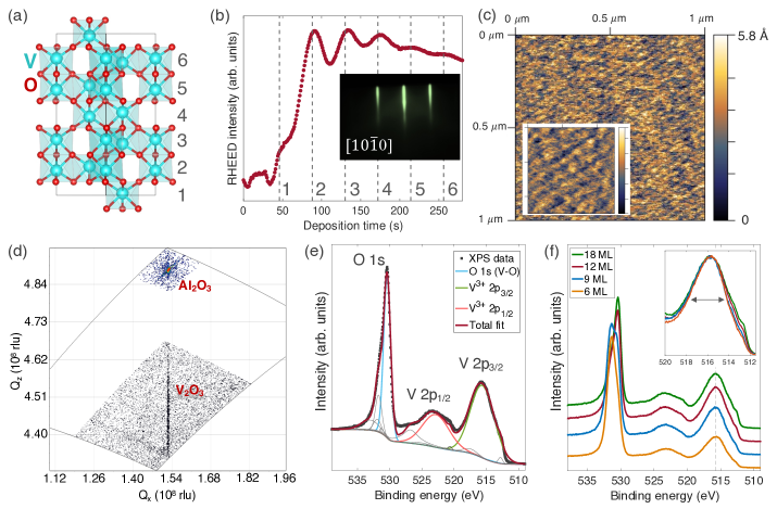
To study novel electronic phenomena in strongly correlated electron systems where many energy scales compete in defining the ground state, there is the need for the growth of high-quality films up to atomic layer precision. In this respect, MBE has shown to be one of the most successful compared to other deposition techniques. By in-situ monitoring the RHEED pattern during the growth, we confirm the epitaxial growth of the ultrathin films on atomically flat - substrates. In addition, intensity oscillations in the RHEED are observed (see Figure 1b) with a periodicity corresponding to the expected growth of one atomic layer, calibrated by the e-beam flux and oxygen pressure. Hence, this corundum material with conventional unit cell (UC) consisting of 6 ML (see Figure 1a) can be grown in a ML fashion, with the ability to control the thickness down to atomic layer precision. This ML growth is also evident from AFM images shown in Figure 1c with estimated step terraces of width nm.
The lattice mismatch of the epitaxial films with the substrates leads to an in-plane compressive strain of . By RSM in reflection, it is shown that the ultrathin films are fully strained in a coherent manner without any strain relaxation. This is due to the fact that all films are below the critical thickness. Hence, in the comparison between the different ultrathin films an identical in-plane lattice constant can be assumed.
Vanadium oxides are known to have a rich phase diagram with many different oxidation states to be stabilized (Wriedt, 1989; Bahlawane and Lenoble, 2014). Therefore, XPS was performed immediately after growth without exposure to ambient air to prevent further oxidation of the films. The core level O - V spectrum is shown in Figure 1e with corresponding curve fitting, confirming the stoichiometry (see Fig. S1 of the Supplemental Material for detailed analysis). Alternatively the binding energy difference between O and V equals eV, which also confirms this stoichiometry (Silversmit et al., 2004). Also note that the broadened linewidth of the V core state can be ascribed to the presence of the electron correlations in the , rather than a mixed oxidation state (Sawatzky and Post, 1979). Moreover, a comparison of core level XPS spectra of the different ultrathin films proves that stoichiometry has been preserved for all thicknesses (see Figure 1f). This excludes any changes as a function of the thickness to be ascribed to a change in the oxygen stoichiometry of the films. Nonetheless, a reducing linewidth of the V core level is observed upon thickness reduction (see inset of Fig. 1f), suggesting the diminishment of the electron correlations, which is indeed the case as will be shown in the subsequent sections.
In contrast to earlier reports on ultrathin films (Luo et al., 2004; Polewczyk et al., 2023), we prove an atomic layer control in the growth of epitaxial coherent and stochiometric in the ultrathin limit. Hence, this permits the study of the intrinsic properties of this archetypical Mott material in the few MLs limit.
III.2 Electronics upon thickness reduction
The intrinsic properties of these ultrathin films at RT were evaluated by the use of transport measurements combined with infrared (IR) spectroscopy. Figure 2 shows the temperature-dependent electrical resistivity of the ultrathin films. First of all, the coherently strained ultrathin films do not show any LT MIT, which has been ascribed to the presence of a large compressive strain and is therefore not related to thickness reduction (Dillemans et al., 2014). The remainder of the manuscript focuses on the room-temperature properties of these ultrathin films.
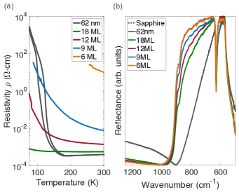
As a reference, to prove the high-quality of the grown thin films, of a relaxed thin film of nm ( UC) is included in Figure 2a. This shows a sharp discontinuous metal-insulator transition at K while the room-temperature resistivity (RTR) equal to cm agrees very well with bulk values (McWhan et al., 1969; McWhan and Remeika, 1970). Upon thickness reduction, the RTR value starts to increase, with an abrupt increase below ML. The RTR of ML is nearly five times larger than the cm RTR value observed in paramagnetic insulating state stabilized for Cr-doped single crystals (McWhan and Remeika, 1970), and epitaxially strained thin films (Homm et al., 2021). Also notice that the ML clearly shows a metallic slope () at RT, which becomes semiconducting below with an increasing slope upon confinement indicating an increased electronic bandgap.
To support these transport measurements, the optical reflectance in near-normal angle incidence is measured using FTIR spectroscopy. The optical reflectance, shown in Figure 2b, has been studied in the mid-infrared range ( cm-1), close to the reststrahlen band of sapphire, that is the infrared band where the reflectance is near-unity and the IR-active phonon resonances appear. Any metallic thin film leads to a damping of this reststrahlen effect, or thus absorbance by the film. It can be seen that this effect reduces upon reducing thickness. Therefore, it can be concluded that the metallicity dissapears below 9 ML thick ultrathin films, in agreement with the transport measurements. A similar spectral change near the reststrahlen band of sapphire can be observed upon LT MIT of the nm thin film (See Fig. S3 in Supplemental Material).
III.3 Bandwidth-controlled transition
is often considered as a key example of a Mott-Hubbard system, that is a purely electronic MIT involving no other degrees of freedom (Imada et al., 1998; Held et al., 2001; Hansmann et al., 2013).
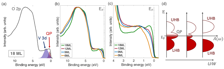
To evaluate the nature of the induced MIT upon thickness reduction, PES was used to probe the changes in the valence band. These spectra consist of a spectral weight derived from the O states in the energy range eV, while close to the Fermi level (), the valence band consists of a broad weight and a sharp coherent QP weight, as shown in Figure 3a. It should be pointed out that the observation of the coherent QP weight required a high-quality pristine surface, otherwise only a faint shoulder could be identified (see Fig. S2 of the Supplemental Material), which indicates the importance of the surface termination and texture. Moreover, the observation of such a large QP weight in a ML ( nm) film is in excellent agreement with the critical thickness estimate of nm required to see the QP weight, as determined through angle-resolved PES experiments on single crystal (Borghi et al., 2009; Rodolakis et al., 2009).
Upon thickness reduction, the QP spectral weight starts to vanish at while simulatenously the V band shifts away from opening an energy gap. This also leads to an energy shift of the oxygen (O ) band. The observed vanishing QP weight with a spectral weight transfer to the V band agrees with the bandwidth-controlled Mott transition behavior derived by DMFT, schematically illustrated in Figure 3d (Georges et al., 1996).
This vanishing QP weight upon confinement can be understood by an orbital-resolved analysis. It was shown that the coherent QP band in the PM phase has a dominant orbital character (Rodolakis et al., 2009; Thees et al., 2021), which transfers its spectral weight to the lower-lying -derived bands upon transition to the PI state (Park et al., 2000; Lo Vecchio et al., 2015; Thees et al., 2021). Now, reducing the thickness causes the electron localization in the out-of-plane orbitals, including mainly . In a single-orbital Hubbard model, this corresponds to a reducing effective bandwidth that triggers a MIT at sufficiently large values with the on-site Coulomb interactions. This scenario has been observed in many other ultrathin oxide films, often referred to as a dimensional-crossover (Yoshimatsu et al., 2010; Gu et al., 2013; Sakai et al., 2013; Gu et al., 2014).
III.4 Confinement as an effective stress component
This confinement-induced (dimensional-crossover) MIT has also been observed in vrious strongly correlated materials (Yoshimatsu et al., 2010; Sakai et al., 2013; Gu et al., 2014; Shiga et al., 2020). However, many of these studies have only considered the electronic nature of this transition, because a structural characterization remains challenging for these few nanometer thick films. In this respect, we have used confocal Raman microscopy and synchrotron X-ray diffraction to study the local interatomic lengths and lattice parameters, respectively.
To monitor local atomic changes in the crystal structure, the Raman active modes have been studied. For , it is well-known that the Raman mode, illustrated in Figure 4b, can be used to probe the short V-V bond along axis, as well as the trigonal distortion driving the RT MIT (Kuroda and Fan, 1977; Poteryaev et al., 2007; Hsu et al., 2023). In particular, a frequency stiffening of the mode observed upon PM to PI MIT is ascribed to an elongated V-V bond where an interelectronic Coulombic force is responsible for the stiffening of the atomic vibration (Yang and Sladek, 1985; Hsu et al., 2023). Taking into account the observed RT MIT in the ultrathin films, the question arises whether the trigonal distortion and the corresponding V-V bond have also been altered upon confinement.
Accordingly, the Raman mode is studied as a function of thickness in the ultrathin films, as shown in Figure 4. To study changes in the phonon dynamics by confinement, the standing wave approximation is proven to be a fruitful approach for many oxides (Senet et al., 1995; Premper et al., 2020; Schober et al., 2020). For the trigonal symmetry, the Raman active modes are non-polar and can be considered to have a quantized wavevector along the out-of-plane Brillouin zone branch () due to confinement. More specifically, the wavevector equals with the number of UCs (6 ML), with the bulk () corresponding to the zone-center and the single UC (6ML) to the zone edge with the out-of-plane lattice constant of the conventional UC. This quantization of the wavevector also leads to a changing eigenenergy, which can be obtained from the dispersion along the branch. The latter was obtained by earlier density functional theory (DFT) calculations (Hsu et al., 2023), and is shown in Fig. 4a.
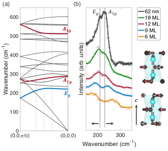
From the calculated dispersion a softening of the in-plane mode can be inferred upon confinement, while the low-frequency shows an initial softening with an abrupt stiffening close to the zone edge . The softening of the mode is confirmed by Raman spectroscopy (see Fig. 4b), albeit that the DFT calculations overestimates the frequency shift. This can be largely explained by the approximation of a sharp boundary condition which prohibits the propagation of the phonon mode across the interface of the film with the substrate. In practice the similarity in crystal structure and phonon spectrum can lead to a broadening of this boundary condition, reducing the effective confinement. On the other hand, a strong frequency hardening is observed for the mode in the Raman spectrum which is inconsistent with the calculated dispersion. This implies that the DFT calculations fail to describe the V-V dimer behavior upon confinement, similar to the PM-PI MIT in bulk which can only be well-described by DMFT (Poteryaev et al., 2007). Moreover, the frequency hardening of the mode upon thickness reduction is very similar to what has been observed in the PM-PI transition, which has been ascribed to a trigonal distortion driving the MIT (Hsu et al., 2023).
At this point, the Raman spectroscopy results exclude any change in symmetry, that means, the RT MIT is isosymmetric. However, this does not exclude an isostructural MIT as often misinterpreted. To verify whether there is a structural change, synchrotron X-ray diffraction was performed on 9 ML and 18 ML ultrathin films to determine the out-of-plane lattice constant. A decrease of the lattice parameter is observed upon thickness reduction from 18 ML to 9 ML, i.e. there is a change in ratio, quantifying the trigonal distortion (See Fig. S5 in Supplemental Material). The relative change of the between 18 ML and 9 ML equals , which is larger than the relative change of for the bulk PM-PI transition. These results confirm the structural nature of this confinement-induced MIT, where a trigonal distortion is triggered upon thickness reduction. This out-of-plane strain component suggests that dimensional confinement acts as a an alternative stress term to alter the trigonal distortion triggering the MIT in .
IV Discussion
Although size confinement has been considered as a chemical pressure in many nanostructures (Lin et al., 2022), such as nanowires (Sun et al., 2020), it remains unnoticed how confinement in thin films and superlattices can lead to an effective out-of-plane pressure. Therefore, we aim to provide an intuitive picture to perceive dimensional confinement as an effective (chemical) pressure. Firstly, by defining pressure in the material as with the bulk modulus, it is evident that an induced pressure exists when there is a change in volume . In particular, considering , a positive pressure corresponds to , while is associated with a negative induced pressure. Reversely, changing the volume in a controlled manner can lead to the inducement of a positive or negative pressure/stress. Now, (chemical) pressure and chemical bonds are intimately related, to the extent that (chemical) pressure has been used as an effective way to identify and quantify the chemical bonds driving the displacive phase transitions (Engelkemier and Fredrickson, 2016; Osman et al., 2018a). Therefore, we propose two views on how a change in pressure () or volume () alters the electrons and their hybridization state. (1) A positive pressure tends to narrow the electron density distribution leading to an orbital expansion to decrease the energy, while negative pressure is accompanied with interatomic delocalization in the regions where covalent bonding occurs (Osman et al., 2018b). (2) Alternatively, by approximating the kinetic (KE) and potential (PE) energies of electrons by the volume dependences and respectively, it becomes immediately evident that a change of volume, or thus a pressure term, can be directly linked to a change in the hybridization (PE/KE) of the electrons (Mellaerts et al., 2022).
In this way, pressure can be perceived as an effective way to alter the electronic charge distribution and their corresponding bonds. Reversely, altering the electronic charge distribution leads to a (chemical) pressure within the crystal. Therefore, dimensional confinement reducing the KE of the electrons occupying the out-of-plane orbitals leads to an increased hybridization (PE/KE), and thus also results in an effective negative pressure term.
Accordingly, the structural changes (out-of-plane strain) discussed in Section III.4 can be explained by an out-of-plane stress that is strongly coupled to the enhanced hybridization of the orbital, which triggers the MIT. Similarly, many other physical phenomena in ultrathin films and heterostructures can be explained as for example, the enhanced tetragonality in various perovskites, such as , , and (Chiu et al., 2022). This involves the electron localization in the out-of-plane -bonding orbitals which favors the hybridization with the O orbitals strengthening the tetragonal distortion (Thomann, 1987; Cohen, 1992). Similarly, it can be expected that the supression/enhancements of octahedral rotations in perovskite-based heterostructures can be explained by the same hybridization preference upon confinement (Garcia-Fernandez et al., 2010).
Consequently, by combining epitaxial substrate-induced strain with thickness control of the ultrathin films, a three-dimensional strain can be imposed albeit that the out-of-plane component is uni-directional whose sign depends on the electronic configuration.
V Conclusions
The achievement of the atomic layered growth of this archetypical Mott material has enabled the observation of an intrinsic MIT at RT induced by dimensional confinement. It has been identified as a clear illustration of a bandwidth-controlled Mott-Hubbard transition with a vanishing QP below ML. Moreover, our findings highlight an enhanced trigonal distortion under confinement, emphasizing the structural component of this MIT. The observed distortion suggests the possibility to model confinement along a specific direction as a negative stress component. Thereby illustrating the potential to leverage thickness control in ultrathin films or heterostructures to induce an effective out-of-plane stress.
Acknowledgements
Part of this work was financially supported by the KU Leuven Research Funds, Project No. C14/21/083, iBOF/21/084, No. KAC24/18/056 and No. C14/17/080, as well as the FWO AKUL/13/19 and AKUL/19/023, and the Research Funds of the INTERREG-E-TEST Project (EMR113) and INTERREG-VL-NL-ETPATHFINDER Project (0559). Part of the computational resources and services used in this work were provided by the VSC (Flemish Supercomputer Center) funded by the Research Foundation Flanders (FWO) and the Flemish government. We acknowledge the use of synchrotron radiation facility at BM25-SpLine at the European Synchrotron and we thanks the Consejo Superior de Investigaciones Cientificas and the Ministerio de Ciencia e Innovacion for financial support under the proposal MA-5601 and projects PIE 2010 6 0E 013 and PIE 2021 60 E 030. J. S. L. acknowledges financial support from the Ministerio de Asuntos Económicos y Transformación Digital (MINECO) through the project PID2020-114192RB-C41. M. M. acknowledges support from Severo Ochoa Programme for Centres of Excellence in R&D (MINCINN, Grant CEX2020-001039-S).
Author contributions
S.M., J.P., J.W.S. and M.H. conceived the conceptual idea and devised the research plan. S.M. executed the synthesis, while in-house diffraction, transport and optical experiments were carried out by S.M., C.B. and W.F.H. XPS, AFM and ARUPS were performed by K.S. Raman spectroscopy was conducted by J.S.L. Synchrotron X-ray diffraction was executed by S.M., W.F.H. and M.M. under guidance of J.S.L. and J.R.Z. All analysis and preparation of the manuscript were done by S.M. All co-authors reviewed and revised the manuscript.
Competing interests
The authors declare no competing interests.
References
- McWhan et al. (1969) D. B. McWhan, T. M. Rice, and J. P. Remeika, Phys. Rev. Lett. 23, 1384 (1969).
- McWhan and Remeika (1970) D. B. McWhan and J. P. Remeika, Phys. Rev. B 2, 3734 (1970).
- Rodolakis et al. (2010) F. Rodolakis, P. Hansmann, J.-P. Rueff, A. Toschi, M. W. Haverkort, G. Sangiovanni, A. Tanaka, T. Saha-Dasgupta, O. K. Andersen, K. Held, M. Sikora, I. Alliot, J.-P. Itié, F. Baudelet, P. Wzietek, P. Metcalf, and M. Marsi, Phys. Rev. Lett. 104, 047401 (2010).
- Homm et al. (2015) P. Homm, L. Dillemans, M. Menghini, B. Van Bilzen, P. Bakalov, C.-Y. Su, R. Lieten, M. Houssa, D. Nasr Esfahani, L. Covaci, F. M. Peeters, J. W. Seo, and J.-P. Locquet, Applied Physics Letters 107, 111904 (2015).
- Homm et al. (2021) P. Homm, M. Menghini, J. W. Seo, S. Peters, and J. P. Locquet, APL Materials 9, 021116 (2021).
- Grieger and Lechermann (2014) D. Grieger and F. Lechermann, Phys. Rev. B 90, 115115 (2014).
- Poteryaev et al. (2007) A. I. Poteryaev, J. M. Tomczak, S. Biermann, A. Georges, A. I. Lichtenstein, A. N. Rubtsov, T. Saha-Dasgupta, and O. K. Andersen, Phys. Rev. B 76, 085127 (2007).
- Pickem et al. (2021) M. Pickem, J. Kaufmann, K. Held, and J. M. Tomczak, Phys. Rev. B 104, 024307 (2021).
- Klebel-Knobloch et al. (2021) B. Klebel-Knobloch, T. Schäfer, A. Toschi, and J. M. Tomczak, Phys. Rev. B 103, 045121 (2021).
- Mellaerts et al. (2021) S. Mellaerts, R. Meng, M. Menghini, V. Afanasiev, J. W. Seo, M. Houssa, and J.-P. Locquet, npj 2D Materials and Applications 5, 65 (2021).
- Ponchut et al. (2011) C. Ponchut, J. M. Rigal, J. Clément, E. Papillon, A. Homs, and S. Petitdemange, Journal of Instrumentation 6, C01069 (2011).
- Wriedt (1989) H. A. Wriedt, Bulletin of Alloy Phase Diagrams 10, 271 (1989).
- Bahlawane and Lenoble (2014) N. Bahlawane and D. Lenoble, Chemical Vapor Deposition 20, 299 (2014).
- Silversmit et al. (2004) G. Silversmit, D. Depla, H. Poelman, G. B. Marin, and R. De Gryse, Journal of Electron Spectroscopy and Related Phenomena 135, 167 (2004).
- Sawatzky and Post (1979) G. A. Sawatzky and D. Post, Phys. Rev. B 20, 1546 (1979).
- Luo et al. (2004) Q. Luo, Q. Guo, and E. G. Wang, Applied Physics Letters 84, 2337 (2004).
- Polewczyk et al. (2023) V. Polewczyk, S. Chaluvadi, D. Dagur, F. Mazzola, S. Punathum Chalil, A. Petrov, J. Fujii, G. Panaccione, G. Rossi, P. Orgiani, G. Vinai, and P. Torelli, Applied Surface Science 610, 155462 (2023).
- Dillemans et al. (2014) L. Dillemans, T. Smets, R. R. Lieten, M. Menghini, C.-Y. Su, and J.-P. Locquet, Applied Physics Letters 104 (2014), 10.1063/1.4866004.
- Imada et al. (1998) M. Imada, A. Fujimori, and Y. Tokura, Rev. Mod. Phys. 70, 1039 (1998).
- Held et al. (2001) K. Held, G. Keller, V. Eyert, D. Vollhardt, and V. I. Anisimov, Phys. Rev. Lett. 86, 5345 (2001).
- Hansmann et al. (2013) P. Hansmann, A. Toschi, G. Sangiovanni, T. Saha-Dasgupta, S. Lupi, M. Marsi, and K. Held, physica status solidi (b) 250, 1251 (2013).
- Borghi et al. (2009) G. Borghi, M. Fabrizio, and E. Tosatti, Phys. Rev. Lett. 102, 066806 (2009).
- Rodolakis et al. (2009) F. Rodolakis, B. Mansart, E. Papalazarou, S. Gorovikov, P. Vilmercati, L. Petaccia, A. Goldoni, J. P. Rueff, S. Lupi, P. Metcalf, and M. Marsi, Phys. Rev. Lett. 102, 066805 (2009).
- Georges et al. (1996) A. Georges, G. Kotliar, W. Krauth, and M. J. Rozenberg, Rev. Mod. Phys. 68, 13 (1996).
- Thees et al. (2021) M. Thees, M.-H. Lee, R. L. Bouwmeester, P. H. Rezende-Gonçalves, E. David, A. Zimmers, F. Fortuna, E. Frantzeskakis, N. M. Vargas, Y. Kalcheim, P. L. Fèvre, K. Horiba, H. Kumigashira, S. Biermann, J. Trastoy, M. J. Rozenberg, I. K. Schuller, and A. F. Santander-Syro, Science Advances 7, eabj1164 (2021).
- Park et al. (2000) J.-H. Park, L. H. Tjeng, A. Tanaka, J. W. Allen, C. T. Chen, P. Metcalf, J. M. Honig, F. M. F. de Groot, and G. A. Sawatzky, Phys. Rev. B 61, 11506 (2000).
- Lo Vecchio et al. (2015) I. Lo Vecchio, L. Baldassarre, F. D’Apuzzo, O. Limaj, D. Nicoletti, A. Perucchi, L. Fan, P. Metcalf, M. Marsi, and S. Lupi, Phys. Rev. B 91, 155133 (2015).
- Yoshimatsu et al. (2010) K. Yoshimatsu, T. Okabe, H. Kumigashira, S. Okamoto, S. Aizaki, A. Fujimori, and M. Oshima, Phys. Rev. Lett. 104, 147601 (2010).
- Gu et al. (2013) M. Gu, J. Laverock, B. Chen, K. E. Smith, S. A. Wolf, and J. Lu, Journal of Applied Physics 113, 133704 (2013).
- Sakai et al. (2013) E. Sakai, M. Tamamitsu, K. Yoshimatsu, S. Okamoto, K. Horiba, M. Oshima, and H. Kumigashira, Phys. Rev. B 87, 075132 (2013).
- Gu et al. (2014) M. Gu, S. A. Wolf, and J. Lu, Advanced Materials Interfaces 1, 1300126 (2014).
- Shiga et al. (2020) D. Shiga, B. E. Yang, N. Hasegawa, T. Kanda, R. Tokunaga, K. Yoshimatsu, R. Yukawa, M. Kitamura, K. Horiba, and H. Kumigashira, Phys. Rev. B 102, 115114 (2020).
- Kuroda and Fan (1977) N. Kuroda and H. Y. Fan, Phys. Rev. B 16, 5003 (1977).
- Hsu et al. (2023) W.-F. Hsu, S. Mellaerts, C. Bellani, P. Homm, N. Uchida, M. Menghini, M. Houssa, J. W. Seo, and J.-P. Locquet, Phys. Rev. Mater. 7, 074606 (2023).
- Yang and Sladek (1985) H. Yang and R. J. Sladek, Phys. Rev. B 32, 6634 (1985).
- Senet et al. (1995) P. Senet, P. Lambin, and A. A. Lucas, Phys. Rev. Lett. 74, 570 (1995).
- Premper et al. (2020) J. Premper, F. O. Schumann, A. Dhaka, S. Polzin, K. L. Kostov, V. Goian, D. Sander, and W. Widdra, physica status solidi (b) 257, 1900650 (2020).
- Schober et al. (2020) A. Schober, J. Fowlie, M. Guennou, M. C. Weber, H. Zhao, J. Iniguez, M. Gibert, J.-M. Triscone, and J. Kreisel, APL Materials 8, 061102 (2020).
- Lin et al. (2022) K. Lin, Q. Li, R. Yu, J. Chen, J. P. Attfield, and X. Xing, Chem. Soc. Rev. 51, 5351 (2022).
- Sun et al. (2020) J. Sun, Q. Li, H. Zhu, Z. Liu, K. Lin, N. Wang, Q. Zhang, L. Gu, J. Deng, J. Chen, and X. Xing, Advanced Materials 32, 2002968 (2020).
- Engelkemier and Fredrickson (2016) J. Engelkemier and D. C. Fredrickson, Chemistry of Materials 28, 3171 (2016).
- Osman et al. (2018a) H. H. Osman, M. A. Salvadó, P. Pertierra, J. Engelkemier, D. C. Fredrickson, and J. M. Recio, Journal of Chemical Theory and Computation 14, 104 (2018a).
- Osman et al. (2018b) H. H. Osman, M. A. Salvadó, P. Pertierra, J. Engelkemier, D. C. Fredrickson, and J. M. Recio, Journal of Chemical Theory and Computation 14, 104 (2018b).
- Mellaerts et al. (2022) S. Mellaerts, J. W. Seo, V. Afanas’ev, M. Houssa, and J.-P. Locquet, Phys. Rev. Mater. 6, 064410 (2022).
- Chiu et al. (2022) C.-C. Chiu, S.-Z. Ho, J.-M. Lee, Y.-C. Shao, Y. Shen, Y.-C. Liu, Y.-W. Chang, Y.-Z. Zheng, R. Huang, C.-F. Chang, C.-Y. Kuo, C.-G. Duan, S.-W. Huang, J.-C. Yang, and Y.-D. Chuang, Nano Letters 22, 1580 (2022).
- Thomann (1987) H. Thomann, Ferroelectrics 73, 183 (1987).
- Cohen (1992) R. E. Cohen, Nature 358, 136 (1992).
- Garcia-Fernandez et al. (2010) P. Garcia-Fernandez, J. A. Aramburu, M. T. Barriuso, and M. Moreno, The Journal of Physical Chemistry Letters 1, 647 (2010).