Reduction of interlayer interaction in multilayer stacking graphene with carbon nanotube insertion: Insights from experiment and simulation
Abstract
The creation of multilayer graphene, while preserving the brilliant properties of monolayer graphene derived from its unique band structure, can expand the application field of graphene into macro scale. However, the energy-favorable AB stacking structure in the multilayer graphene induces a strong interlayer interaction and alters the band structure. Consequently, the intrinsic properties of each monolayer are degraded. In this work, we insert carbon nanotubes (CNT) as nanospacers to modulate the microstructure of multilayer stacking graphene. Nanospacers can increase interlayer distance and reduce interlayer interaction. The graphene/CNT stacking structure is experimentally fabricated using a dry transfer method in a layer-by-layer manner. Raman spectroscopy verifies the reduction in interlayer interaction within the stacking structure. Atomic force microscopy scanning shows an increase in the interlayer distance, which can explain the weakening of interlayer interactions. The microstructure of the stacked graphene and CNTs is studied by molecular dynamics simulation to systematically investigate the effect of CNT insertion. We found that the distribution distance, size, and arrangement of the CNT can modulate the interlayer distance. These results will help to understand and improve the properties of the composite systems consisting of graphene and CNTs.
keywords:
American Chemical Society, LaTeXOUKobayashi] Department of Applied Physics, Graduate School of Engineering, Osaka University, Suita, Osaka 565-0871, Japan OUKobayashi] Department of Applied Physics, Graduate School of Engineering, Osaka University, Suita, Osaka 565-0871, Japan OUMori] Department of Precision Engineering, Graduate School of Engineering, Osaka University, Suita, Osaka 565-0871, Japan OUMori] Department of Precision Engineering, Graduate School of Engineering, Osaka University, Suita, Osaka 565-0871, Japan NTT] NTT Basic Research Laboratories, NTT Corporation, Kanagawa 243-0198, Japan NTT] NTT Basic Research Laboratories, NTT Corporation, Kanagawa 243-0198, Japan OUMori] Department of Precision Engineering, Graduate School of Engineering, Osaka University, Suita, Osaka 565-0871, Japan OUMori] Department of Precision Engineering, Graduate School of Engineering, Osaka University, Suita, Osaka 565-0871, Japan OUKobayashi] Department of Applied Physics, Graduate School of Engineering, Osaka University, Suita, Osaka 565-0871, Japan \phone+81-06-6879-7833 \fax+81-06-6879-7863 \abbreviationsIR,NMR,UV
![[Uncaptioned image]](/html/2312.03440/assets/x1.png)
1 Introduction
Graphene is a material with excellent electrical, thermal, and optical properties1, 2, 3, 4, 5 and broad prospects for applications6, 7, 8, 9, 10. Monolayer graphene has a unique band structure with a linear electronic dispersion, which results in high carrier mobility1, 2 and uniform light absorption of a wide range of wavelengths3, 7. Moreover, multilayer graphene shows high electrical and thermal conductance and light absorption with the increase of layer number11, 12, 13. The screening effect of multilayer graphene also prevents the degradation of the electronic transportation properties caused by the surrounding environment, including charge impurities and substrate roughness13. However, the energetically favorable AB stacking in multilayer graphene leads to a strong interlayer interaction, which results in a parabolic electronic dispersion14. The intrinsic properties of monolayer graphene, including high carrier mobility, are undermined. Therefore, reducing interlayer interactions allows each layer to exhibit monolayer-graphene-like properties, thereby enhancing the overall material performance of multilayer graphene.
A feasible approach for suppressing interlayer interactions is to increase the interlayer distance. Theoretical analysis has proven that interlayer coupling decreases with the increase of interlayer distance15, 16. Experimental observations have shown that the intercalation of small molecules such as and into multilayer graphene reduces the interlayer interaction 15, 17. Nanospacers such as nanodiamonds, carbon nanotubes (CNTs), and nanofibers can also prevent restacking and reduce the interlayer interaction in graphene sponge structures18, 19, 20. Compared with other nanospacers, the CNT is another allotrope of carbon with the same hybridized structure as graphene, which does not introduce impurities and dopants from other elements. Moreover, the graphene and CNT composite system has excellent electronic properties and a high surface-to-volume ratio, which provides widespread potential applications in electronic devices21, 22, 23, 24, 25, energy storage26, 27, 28, chemical catalyst29, 30, 18, 31, and water treatment32, 33.
The microstructure of the graphene and CNT composite system has a remarkable impact on properties. The addition of CNTs with a diameter of several nanometers can markedly increase the interlayer distance and reduce interlayer interaction16. Consequently, each graphene layer is remarkably separated and almost suspended. The benefits of suspended graphene include ultrahigh carrier mobility and ballistic transport34, 6, 35, 36, 37. However, the single-atom layer structure of graphene results in its low stiffness to bending deformation38. The adsorption interaction among graphene layers results in the bending of graphene and a decrease in interlayer distance39, 40, 41, 42, 43. Thus, negative factors, including strong interlayer coupling, electron scattering, and a decrease in the surface-to-volume ratio, will appear. Thus, investigating the real effect of CNT insertion on the microstructure of the graphene and CNT composite system is necessary to comprehensively understand and optimize their interaction. In previous experimental studies, the graphene and CNT composite system was usually fabricated through a random mixture of liquid phases, making it difficult to control the layer number and to ensure the CNT insertion between all graphene layers18, 19. Therefore, a new fabrication approach with enhanced structural controllability must be developed. In addition, molecular dynamics (MD) was employed to investigate the mechanical properties of a multilayer graphene and CNT stacking structure, including elastic constants40. The deformation of CNT encapsulated by two graphene layers is also studied theoretically43. However, the influencing factors that determine the microstructure, such as the size and distribution of CNTs, have not been systematically studied.
In this study, we investigated the multilayer graphene stacking structure with CNT insertion through experiments and simulations. First, we experimentally fabricated such a graphene/CNT stacking structure using a dry transfer method. Highly controlled stacking structures with defined graphene layer numbers are achieved by alternately transferring monolayer graphene and depositing CNTs. Raman spectroscopy confirms a weak interlayer interaction, and atomic force microscopy (AFM) verifies an increase in interlayer distance. Then, MD simulations were conducted to study the microstructure. A systematic investigation of the effect of CNT insertion on the interlayer distance was also conducted, including the CNT distance, diameter, and arrangement. A configuration transition from interlayer suspension to interlayer adsorption with increasing CNT distance was observed. The critical transition distance increases with CNT diameter. Our study provides support for controlling the microstructure of the graphene and CNT composite system and enhancing the material properties.
2 Methods
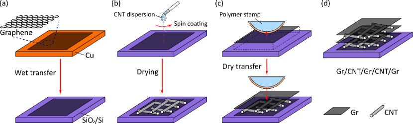
Experimental methods. The graphene/CNT stacking structure was fabricated experimentally by using the dry transfer method (Figure 1). The monolayer graphene was prepared on Cu foil by chemical vapor deposition (CVD)44. The graphene was transferred onto a silicon substrate (with 300 nm oxide layer) using the wet transfer method with a poly(methyl methacrylate) (PMMA) film 45, 46, as shown in Figure 1a. This step can make graphene on the silicon surface easier to be manipulated in subsequent experiments. Then, the CNT nanospacers were scattered on the graphene surface by spin coating the dispersion of CNT (Figure 1b). The CNT was synthesized by using the arc-discharge method and dispersed in ethanol with a concentration of 0.05 mg/mL (Meijo Nano Carbon, FH-P). The CNT is single walled with a diameter of nm according to the manufacturer’s information. The sample was placed on a hot plate of 90 ∘C to let ethanol evaporate. The areal density of the CNT was increased by repeated spin coating for designated times. The second graphene layer was picked up from the Si substrate, which is prepared by the same wet transfer method and covered onto the CNT nanospacer by using the dry transfer method using polymer stamps47, 48, 49, as shown in Figure 1c. The successful transfer of the second layer can be confirmed by using an optical microscope (Figure S1 in Supporting Information). A multilayer stacking structure can be fabricated by repeating the spin coating of CNT and graphene using a dry transfer process (Figure 1d). Raman spectroscopy was performed using a objective lens with a laser excitation of 532 nm and a typical spot diameter of (Horiba, LabRAM HR-800). AFM measurements were conducted in the dynamic force mode (Hitachi High-Tech, AFM5100N).

Simulation method. We conducted MD simulations using LAMMPS program to provide more details on the microstructure of graphene/CNT stacking and the influence of various parameters of CNTs50. The simulation model is shown in Figure 2. Two parallelly aligned CNTs are encapsulated in two graphene layers (Figure 2a). The periodic boundary condition is added in the in-plane and directions to simulate the CNT array aligned at equal distances of infinite length. The width of the graphene layers and the length of CNTs are both nm in the simulation system. The distance of the CNTs is , and the length of the graphene layers is (Figure 2b). The graphene interlayer distance of the initial configuration , where is the diameter of the CNTs, and is the interlayer distance between graphene layers in graphite. Here, we took nm, 0.68 nm, 1.08 nm, and 1.35 nm, and nm. The AIREBO potential51 was used to describe the short-range interaction among carbon atoms. The long-range van der Waals (vdW) interaction among carbon atoms in graphene layers and CNTs is described by using the Lennard-Jones (LJ) potential
| (1) |
where is the distance between two atoms. The parameter is the depth of the potential well, and is the zero-energy point and balance distance between graphene layers in graphite51. In inducing a vdW interaction between the upper and lower graphene, we set the cutoff radius for long-range interactions larger than the interlayer distance (). This process results in increased computational time for simulation. The lower graphene is constrained by a virtual LJ wall to simulate the adsorption effect of the layer on the Si substrate52, 53, 54. The energy of the wall-atom interaction is calculated as follows:
| (2) |
where is the distance between the carbon atom and the virtual LJ wall. The adhesion energy55, 56, 57 is , and the balance distance between graphene and substrate58, 59 is nm. The areal density of carbon atoms is . The system is relaxed in the NVT ensemble at 300 K with a simulation timestep of 1 fs until the energy and configuration of the system reach equilibrium. Thus, the energy-favorable configuration is obtained.
3 Results and discussion

Raman spectroscopy first validates the weakening of the interlayer interaction of graphene by CNT insertion (Figure 3). Typical Raman spectra of monolayer graphene (Gr) exhibit the D peak (), G peak (), and peak ()60. The D peak is affected by crystal defects60. The G peak intensity increases with the graphene layer number61, 62. The peak relative intensity is sensitive to the graphene layer number and stacking order63, 64. For monolayer graphene, the intensity ratio of the peak to the G peak () is generally 63, 64, 65, 35. The ratio decreases with the increase of the layer number for the AB stacking multilayer graphene due to the strong interlayer interaction and altered band structure with parabolic dispersion. A relatively high ratio can be observed in the random stacking multilayer graphene66, 67, 60. In random stacking graphene, the interlayer interaction is weaker than the AB stacking graphene, and the interlayer distance is slightly larger15. The band structure of the random stacking graphene resembles the monolayer graphene with linear dispersion14, 16. The CNT also has the D peak, G peak, and peak at similar positions. For single-walled CNTs, the G peak splits into two sub-peaks: (at 1572 ) and (at 1592 )21. In our sample, the monolayer graphene shows , which is slightly lower than the typical value because of some multilayer islands on the CVD graphene and the doping from substrate impurities and PMMA residue. In the case of bilayer graphene (Gr/Gr), the ratio remarkably decreases to 0.59, which is consistent with the previous study61, 66, 67. The peak is also lower than the peak in monolayer graphene after adding CNTs (Gr/CNT). The G peak exhibits an asymmetric shape because of the overlapping of the G peak from graphene and split and from CNTs. For the bilayer graphene/CNT stacking structure (Gr/CNT/Gr), the contribution from CNT should be removed when calculating . We used a three-peak fitting approach to extract the graphene component in the G peak. The fitting result is shown in the subgraph of Figure 3a, and the intensity of the graphene G peak component is referred to as . The CNT also shows a peak at . The to G ratio is for CNT on (Figure S2 in Supporting Information). The proportion of the and peak within the G peak is remarkably smaller than that of the peak (). Therefore, we neglected the peak induced by the CNT in the total peak of the stacking structure. The of Gr/CNT/Gr is higher than that of two directly stacked graphene layers (Gr/Gr). This result demonstrates a reduction of interlayer interaction in the Gr/CNT/Gr structure because of the insertion of CNTs.
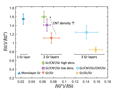
We further investigated the impact of CNT density and layer number on the interlayer interaction by Raman spectroscopy (Figure 4). The intensity ratio of the G peak to the substrate silicon peak at is used to indicate the layer number of graphene, and the interlayer interaction was evaluated by the . Multiple data points were obtained by measuring different sample positions. The average value and standard error were calculated, and the results are plotted in Figure 4. All point version is shown in Figure S3 in Supporting Information. The increase of indicates the increase of layer number from Gr to Gr/Gr and trilayer graphene (Gr/Gr/Gr). The ratio does not increase linearly with the number of layers. Previous studies have found that in randomly stacking bilayer graphene66, 67, a phonon resonance enhancement and an increase in the G peak intensity are observed when the twist angle between the two layers . Our multilayer graphene is stacked from polycrystalline CVD graphene with randomly oriented grains, which is also random stacking. Thus, a further increase in is observed. Comparing the Gr/Gr and Gr/CNT/Gr with different CNT densities, we observed lower values of with increasing density. Previous studies observed a weaker G peak in suspended graphene compared with graphene on a substrate35, 68, which is attributed to the effect of substrate. CNTs increase the interlayer distance and make some part of the upper graphene nearly suspended. More CNT nanospacers separate more parts of graphene layers, and the average interlayer distance increases in the measured spots. The partial suspension of graphene contributes to the decrease in . Then, the high CNT density was kept, and the stacking structure of trilayer graphene and CNTs (Gr/CNT/Gr/CNT/Gr) as well as the Gr/Gr/Gr was also fabricated (Figure 4). The ratio in the Gr/CNT/Gr/CNT/Gr is higher than that of the Gr/Gr/Gr, demonstrating the continued effectiveness of CNT insertion with increasing layer number.

The insertion of CNT can reduce the interlayer interaction. The reduction can be attributed to the alteration of the microstructure by increasing the interlayer distance. The AFM measurement was employed to analyze the microstructure of the samples (Figure 5). The AFM images of the CNT distribution with low and high densities on Gr/CNT are shown in Figure 5a,b and Figure S4. The length of the CNTs ranges , with a diameter of nm. The measured diameter is higher than the parameters provided by the manufacturer. The surfactant is added when dissolving the CNTs in ethanol. The surfactant molecules adsorbed on the CNT can increase the measured diameter. The portion without adsorbed surfactant may lead to the attraction among CNTs, forming CNT bundles, which can also cause an increase in the measured diameter. The AFM images of the Gr/CNT/Gr with low and high densities are shown in Figures 5c and d, respectively. By comparing the cross-sectional images (Figures 5e,f), the two CNTs with a larger distance show a lower thickness () of the region among CNTs. When the distance is nm, the height of the region among CNTs is 0.76 nm. When the distance between the CNTs is nm, the height of the region is nm, which is remarkably higher than the thickness of two graphene layers. Therefore, the upper layer of graphene is supported by the CNTs to form a partially suspended structure. Figure 5g illustrates the relationship between the distance of CNTs and the height of the upper-layer graphene at multiple cross-sections. As the distance between the CNTs increases, gradually decreases. A theoretical study has reported that increasing the interlayer distance can weaken interlayer coupling and alter the band structure of multilayer graphene which is comparable with that of a single layer with linear dispersion16. CNTs induce the partial suspension of graphene, thereby increasing the interlayer distance. This finding explains the observed reduction of interlayer interactions in Raman spectroscopy.
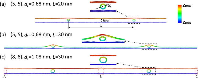

We conducted MD simulations of the graphene/CNT stacking structure to investigate the influencing factors of the CNT in detail and to study the microstructure comparatively through AFM observation. The MD simulation can easily control the CNT diameter and area density compared with the experiment. The intuitive microstructure figures can be output at a low cost compared with sample fabrication and AFM scanning. Figure 6a–c shows three examples of the MD simulation with different CNT diameters and CNT distances ( nm, nm, nm, nm, and nm, nm). In the first case (Figure 6a), the upper graphene is suspended among the CNTs, but it exhibits a slight curvature after relaxation, which is due to the vdW attraction between the layers. If the distance is increased to nm (Figure 6b), then the upper graphene is adsorbed on the lower graphene layer with evident bending deformation near the CNTs. The interlayer distance of the two graphene layers is 0.34 nm, which is close to the spacing of carbon layers in graphite. If the distance is fixed and increases to nm (Figure 6c), then the upper graphene stays in suspension, which is similar to the first case.
We performed additional simulations by varying the chirality indices, diameters, and distances between the CNTs (Figure 7). The final configurations are classified into two categories: upper graphene suspension and layer adsorption. The minimum interlayer distance can distinguish between the two configurations. It is calculated by averaging the distance between the graphene layers at the midpoint and two ends (Figure 6c). In the case of the same when the distance is small (Figure 7a), the approaches the initial spacing , indicating that the upper graphene layer remains suspended. As the CNT distance gradually increases and surpasses a critical value, the interlayer distance abruptly decreases to 0.34 nm, indicating the occurrence of interlayer adsorption. As the diameter increases, the interlayer distance in the suspended graphene configuration also increases. A large CNT diameter also increases the critical CNT distance () at which the adsorption configuration appears (Figure 7b). The relation between and is approximately linear. Linear regression is conducted (dashed line in Figure 7b). In the experiments, CNTs are randomly distributed, and crossing CNTs are observed. Therefore, stacking structures with crossing CNTs were also simulated (triangles in Figure 7a). The model is shown in Figure S5. Compared with parallelly aligned CNTs, the crossing CNTs can increase the critical distance for configuration transition from suspension to adsorption.
The transition of configuration from suspension to adsorption configuration implies a change in energy. The potential energy of the simulation system is composed of the internal energy of each graphene layer and CNT described by the AIREBO potential, the vdW energy between the different graphene layers and CNTs described by the LJ potential, and the vdW energy between the lower graphene layer and the substrate. The internal energy is influenced by the positional changes of carbon atoms, i.e., deformation of graphene, and CNTs. The vdW energy is determined by the distance between different graphene layers and CNTs (Eq. 1). Considering that the lower graphene layer remains nearly flat without remarkable deformation, no evident change in its internal energy and vdW energy with substrate is observed. The number of atoms in the CNT is smaller than the number of atoms in the graphene layer, and the change in vdW energy induced by CNT deformation is negligible. Thus, the configuration of the system is determined by the competition between the internal energy of the upper graphene and the vdW energy between the two graphene layers. In the suspended configuration, the upper graphene layer has insignificant deformation, resulting in a minor increase in internal energy. However, a higher vdW potential energy contains a larger interlayer distance (Figure S6). For the bilayer adsorption configuration, the vdW energy is minimized with an interlayer distance nm. However, the obstructive effect of CNT induces graphene deformation, leading to the bending of angles between C-C bonds and an increase in internal energy. The collapse of CNTs also appears with an ellipse cross-section (see Figure 6b), which causes an extra increase in internal energy43. The adsorption configuration contains higher internal energy and lower vdW energy compared with the suspended configuration.
Experiments and MD simulations have simultaneously discovered that as the distance between CNTs increases, the structure transitions from an upper graphene layer suspension to an interlayer adsorption structure. The trend can qualitatively match, but the quantitative comparison has discrepancies. The critical length obtained by the MD simulation is nm for CNTs with a diameter range of nm. Based on the predictions from linear regression analysis, the critical length of CNTs with diameters ranging from nm, which corresponds to the CNT diameters in the experiment, is estimated to be nm. The experimental observations show graphene suspension with a CNT distance of 700 nm, which is larger than the prediction based on MD simulation. Several factors benefit from the suspension of graphene in the experiment. In ethanol dispersion, surfactant is added to promote CNT dissolution. The surfactant molecules wrap the surface of CNTs by non-covalent interaction, which weakens the interaction between carbon monolayers of graphene and CNTs69. The distance between CNTs and graphene layers (Figure 2b) is increased because surfactant molecules serve as spacers. Thus, the critical distance is increased. Moreover, the CNT is randomly distributed on the surface. The MD simulation indicates that crossing CNTs can increase the critical distance (Figure 7a). The CNTs may also aggregate to form CNT bundles where the surfactant is not covered. This effect is similar to the increase in CNT diameter, leading to an increase in .
4 Conclusions
We study the effect of CNT insertion to reduce the interlayer interaction in multilayer graphene. The stacking structure of graphene and CNT is experimentally fabricated. Raman spectroscopy and AFM measurement verify the reduction of interlayer interaction and increase of interlayer distance. In addition, MD simulations are conducted to systematically study the influencing factors. The graphene/CNT stacking structure exhibits two stable configurations: the upper-layer suspension and interlayer adsorption. The distance, diameter, and arrangement of the CNTs determine the selection of the stable structure. Our research contributes not only to the enhanced property of multilayer graphene but also to a comprehensive understanding of the microstructure of the graphene/CNT composite system to facilitate functional enhancement for wider application fields.
This research was supported by JSPS KAKENHI (No. JP15H05866, JP17H05336, JP17H02745, JP19H04545, and JP21H01763), JST SPRING (No. JPMJSP2138), and Murata Research Foundation. The MD simulation of this research work utilized the computing resources of the Institute of Solid State Physics supercomputer center at the University of Tokyo.
This material is available free of charge via the Internet.
References
- Novoselov et al. 2005 Novoselov, K. S.; Geim, A. K.; Morozov, S. V.; Jiang, D.; Katsnelson, M. I.; Grigorieva, I. V.; Dubonos, S. V.; Firsov, A. A. Two-dimensional gas of massless Dirac fermions in graphene. Nature 2005, 438, 197–200
- Meric et al. 2008 Meric, I.; Han, M. Y.; Young, A. F.; Ozyilmaz, B.; Kim, P.; Shepard, K. L. Current saturation in zero-bandgap, top-gated graphene field-effect transistors. Nature Nanotechnology 2008, 3, 654–659
- Mak et al. 2008 Mak, K. F.; Sfeir, M. Y.; Wu, Y.; Lui, C. H.; Misewich, J. A.; Heinz, T. F. Measurement of the Optical Conductivity of Graphene. Physical Review Letters 2008, 101, 196405–1–196405–4
- Balandin et al. 2008 Balandin, A. A.; Ghosh, S.; Bao, W.; Calizo, I.; Teweldebrhan, D.; Miao, F.; Lau, C. N. Superior Thermal Conductivity of Single-Layer Graphene. Nano Letters 2008, 8, 902–907
- Lee et al. 2008 Lee, C.; Wei, X.; Kysar, J. W.; Hone, J. Measurement of the Elastic Properties and Intrinsic Strength of Monolayer Graphene. Science 2008, 321, 385–388
- Bunch et al. 2007 Bunch, J. S.; van der Zande, A. M.; Verbridge, S. S.; Frank, I. W.; Tanenbaum, D. M.; Parpia, J. M.; Craighead, H. G.; McEuen, P. L. Electromechanical Resonators from Graphene Sheets. Science 2007, 315, 490–493
- Koppens et al. 2014 Koppens, F. H. L.; Mueller, T.; Avouris, P.; Ferrari, A. C.; Vitiello, M. S.; Polini, M. Photodetectors based on graphene, other two-dimensional materials and hybrid systems. Nature Nanotechnology 2014, 9, 780–793
- Raccichini et al. 2015 Raccichini, R.; Varzi, A.; Passerini, S.; Scrosati, B. The role of graphene for electrochemical energy storage. Nature Materials 2015, 14, 271–279
- Deng and Berry 2016 Deng, S.; Berry, V. Wrinkled, rippled and crumpled graphene: an overview of formation mechanism, electronic properties, and applications. Materials Today 2016, 19, 197–212
- Akinwande et al. 2017 Akinwande, D.; Brennan, C. J.; Bunch, J. S.; Egberts, P.; Felts, J. R.; Gao, H.; Huang, R.; Kim, J.-S.; Li, T.; Li, Y. et al. A review on mechanics and mechanical properties of 2D materials—Graphene and beyond. Extreme Mechanics Letters 2017, 13, 42–77
- Zhu et al. 2014 Zhu, S.-E.; Yuan, S.; Janssen, G. C. A. M. Optical transmittance of multilayer graphene. EPL 2014, 108, 17007–p1–17007–p4
- Shen et al. 2016 Shen, X.; Wang, Z.; Wu, Y.; Liu, X.; He, Y.-B.; Kim, J.-K. Multilayer Graphene Enables Higher Efficiency in Improving Thermal Conductivities of Graphene/Epoxy Composites. Nano Letters 2016, 16, 3585–3593
- Negishi et al. 2020 Negishi, R.; Wei, C.; Yao, Y.; Ogawa, Y.; Akabori, M.; Kanai, Y.; Matsumoto, K.; Taniyasu, Y.; Kobayashi, Y. Turbostratic Stacking Effect in Multilayer Graphene on the Electrical Transport Properties. Physica Status Solidi B 2020, 257, 1900437
- Latil et al. 2007 Latil, S.; Meunier, V.; Henrard, L. Massless fermions in multilayer graphitic systems with misoriented layers: Ab initio calculations and experimental fingerprints. Physical Review B 2007, 76, 201402–1–201402–4
- Kinoshita et al. 2017 Kinoshita, H.; Jeon, I.; Maruyama, M.; Kawahara, K.; Terao, Y.; Ding, D.; Matsumoto, R.; Matsuo, Y.; Okada, S.; Ago, H. Highly Conductive and Transparent Large-Area Bilayer Graphene Realized by MoCl Intercalation. Advanced Materials 2017, 29, 1702141
- Denner et al. 2020 Denner, M. M.; Lado, J. L.; Zilberberg, O. Antichiral states in twisted graphene multilayers. Physical Review Research 2020, 2, 043190–1–043190–8
- Lin et al. 2021 Lin, Y.-C.; Motoyama, A.; Solís-Fernández, P.; Matsumoto, R.; Ago, H.; Suenaga, K. Coupling and Decoupling of Bilayer Graphene Monitored by Electron Energy Loss Spectroscopy. Nano Letters 2021, 21, 10386–10391
- Zhang et al. 2012 Zhang, D.; Yan, T.; Shi, L.; Peng, Z.; Wen, X.; Zhang, J. Enhanced capacitive deionization performance of graphene/carbon nanotube composites. Journal of Materials Chemistry 2012, 22, 14696–14704
- Xu et al. 2021 Xu, Z.; Nakamura, S.; Inoue, T.; Nishina, Y.; Kobayashi, Y. Bulk-scale synthesis of randomly stacked graphene with high crystallinity. Carbon 2021, 185, 368–375
- Xu et al. 2022 Xu, Z.; Inoue, T.; Nishina, Y.; Kobayashi, Y. Stacking order reduction in multilayer graphene by inserting nanospacers. Journal of Applied Physics 2022, 132, 174305–1–174305–12
- Paulus et al. 2013 Paulus, G. L. C.; Wang, Q. H.; Ulissi, Z. W.; McNicholas, T. P.; Vijayaraghavan, A.; Shih, C.-J.; Jin, Z.; Strano, M. S. Charge Transfer at Junctions of a Single Layer of Graphene and a Metallic Single Walled Carbon Nanotube. Small 2013, 9, 1954–1963
- Liao et al. 2019 Liao, Y.; Mustonen, K.; Tulić, S.; Skákalová, V.; Khan, S. A.; Laiho, P.; Zhang, Q.; Li, C.; Monazam, M. R. A.; Kotakoski, J. et al. Enhanced Tunneling in a Hybrid of Single-Walled Carbon Nanotubes and Graphene. ACS Nano 2019, 13, 11522–11529
- Liu et al. 2015 Liu, Y.; Wang, F.; Wang, X.; Wang, X.; Flahaut, E.; Liu, X.; Li, Y.; Wang, X.; Xu, Y.; Shi, Y. et al. Planar carbon nanotube–graphene hybrid films for high-performance broadband photodetectors. Nature Communications 2015, 6, 8589
- Kholmanov et al. 2015 Kholmanov, I. N.; Magnuson, C. W.; Piner, R.; Kim, J.; Aliev, A. E.; Tan, C.; Kim, T. Y.; Zakhidov, A. A.; Sberveglieri, G.; Baughman, R. H. et al. Optical, Electrical, and Electromechanical Properties of Hybrid Graphene/Carbon Nanotube Films. Advanced Materials 2015, 27, 3053–3059
- Shang et al. 2022 Shang, K.; Yang, T.; Guo, C.; Pu, X.; Zhang, Y.; Lu, X.; He, C.; Zhou, J.; Wu, L.; Yu, B. et al. Interfacial Enhanced 1D–2D Composite toward Mechanically Robust Strain Sensors. Advanced Materials Interfaces 2022, 9, 2201201
- Yu et al. 2014 Yu, D.; Goh, K.; Wang, H.; Wei, L.; Jiang, W.; Zhang, Q.; Dai, L.; Chen, Y. Scalable synthesis of hierarchically structured carbon nanotube–graphene fibres for capacitive energy storage. Nature Nanotechnology 2014, 9, 555–562
- Wang et al. 2020 Wang, Y.; Zhang, Y.; Wang, G.; Shi, X.; Qiao, Y.; Liu, J.; Liu, H.; Ganesh, A.; Li, L. Direct Graphene-Carbon Nanotube Composite Ink Writing All-Solid-State Flexible Microsupercapacitors with High Areal Energy Density. Advanced Functional Materials 2020, 30, 1907284
- Yu and Dai 2010 Yu, D.; Dai, L. Self-Assembled Graphene/Carbon Nanotube Hybrid Films for Supercapacitors. The Journal of Physical Chemistry Letters 2010, 1, 467–470
- Xu et al. 2020 Xu, Y.; Deng, P.; Chen, G.; Chen, J.; Yan, Y.; Qi, K.; Liu, H.; Xia, B. Y. 2D Nitrogen-Doped Carbon Nanotubes/Graphene Hybrid as Bifunctional Oxygen Electrocatalyst for Long-Life Rechargeable Zn–Air Batteries. Advanced Functional Materials 2020, 30, 1906081
- Li et al. 2012 Li, Y.; Zhou, W.; Wang, H.; Xie, L.; Liang, Y.; Wei, F.; Idrobo, J.-C.; Pennycook, S. J.; Dai, H. An oxygen reduction electrocatalyst based on carbon nanotube–graphene complexes. Nature Nanotechnology 2012, 7, 394–400
- Shi et al. 2012 Shi, C.; Meng, J.; Deng, C. Facile synthesis of magnetic graphene and carbon nanotube composites as a novel matrix and adsorbent for enrichment and detection of small molecules by MALDI-TOF MS. Journal of Materials Chemistry 2012, 22, 20778–20785
- Tristán-López et al. 2013 Tristán-López, F.; Morelos-Gómez, A.; Vega-Díaz, S. M.; García-Betancourt, M. L.; Perea-López, N.; Elías, A. L.; Muramatsu, H.; Cruz-Silva, R.; Tsuruoka, S.; Kim, Y. A. et al. Large Area Films of Alternating Graphene–Carbon Nanotube Layers Processed in Water. ACS Nano 2013, 7, 10788–10798
- Yin et al. 2020 Yin, Z.; Cui, C.; Chen, H.; Duoni,; Yu, X.; Qian, W. The Application of Carbon Nanotube/Graphene-Based Nanomaterials in Wastewater Treatment. Small 2020, 16, 1902301
- Du et al. 2008 Du, X.; Skachko, I.; Barker, A.; Andrei, E. Y. Approaching ballistic transport in suspended graphene. Nature Nanotechnology 2008, 3, 491–495
- Berciaud et al. 2009 Berciaud, S.; Ryu, S.; Brus, L. E.; Heinz, T. F. Probing the Intrinsic Properties of Exfoliated Graphene: Raman Spectroscopy of Free-Standing Monolayers. Nano Letters 2009, 9, 346–352
- Meyer et al. 2007 Meyer, J. C.; Geim, A. K.; Katsnelson, M. I.; Novoselov, K. S.; Booth, T. J.; Roth, S. The structure of suspended graphene sheets. Nature 2007, 446, 60–63
- Bolotin et al. 2008 Bolotin, K.; Sikes, K.; Jiang, Z.; Klima, M.; Fudenberg, G.; Hone, J.; Kim, P.; Stormer, H. Ultrahigh electron mobility in suspended graphene. Solid State Communications 2008, 146, 351–355
- Lindahl et al. 2012 Lindahl, N.; Midtvedt, D.; Svensson, J.; Nerushev, O. A.; Lindvall, N.; Isacsson, A.; Campbell, E. E. B. Determination of the Bending Rigidity of Graphene via Electrostatic Actuation of Buckled Membranes. Nano Letters 2012, 12, 3526–3531
- Fonseca et al. 2019 Fonseca, A. F.; Dantas, S. O.; Galvão, D. S.; Zhang, D.; Sinnott, S. B. The structure of graphene on graphene/C/Cu interfaces: a molecular dynamics study. Nanotechnology 2019, 30, 505707
- Menon and Buldum 2020 Menon, V.; Buldum, A. Mechanical properties of graphene-CNT van der Waals heterostructures: a molecular dynamics study. Nanotechnology 2020, 31, 455707
- Varillas and Frank 2021 Varillas, J.; Frank, O. Wrinkle development in graphene sheets with patterned nano-protrusions: A molecular dynamics study. Carbon 2021, 173, 301–310
- Haraguchi et al. 2023 Haraguchi, K.; Iwakami, S.; Ohba, T. Fabrication of Fullerene-Pillared Porous Graphene and Its Water Vapor Adsorption. The Journal of Physical Chemistry C 2023, 127, 12333–12341
- Xu and Jiang 2023 Xu, T.; Jiang, J. On the configuration of the graphene/carbon nanotube/graphene van der Waals heterostructure. Physical Chemistry Chemical Physics 2023, 25, 5066–5072
- Brown et al. 2014 Brown, L.; Lochocki, E. B.; Avila, J.; Kim, C.-J.; Ogawa, Y.; Havener, R. W.; Kim, D.-K.; Monkman, E. J.; Shai, D. E.; Wei, H. I. et al. Polycrystalline Graphene with Single Crystalline Electronic Structure. Nano Letters 2014, 14, 5706–5711
- Li et al. 2009 Li, X.; Zhu, Y.; Cai, W.; Borysiak, M.; Han, B.; Chen, D.; Piner, R. D.; Colombo, L.; Ruoff, R. S. Transfer of Large-Area Graphene Films for High-Performance Transparent Conductive Electrodes. Nano Letters 2009, 9, 4359–4363
- Suk et al. 2011 Suk, J. W.; Kitt, A.; Magnuson, C. W.; Hao, Y.; Ahmed, S.; An, J.; Swan, A. K.; Goldberg, B. B.; Ruoff, R. S. Transfer of CVD-Grown Monolayer Graphene onto Arbitrary Substrates. ACS Nano 2011, 5, 6916–6924
- Castellanos-Gomez et al. 2014 Castellanos-Gomez, A.; Buscema, M.; Molenaar, R.; Singh, V.; Janssen, L.; van der Zant, H. S. J.; Steele, G. A. Deterministic transfer of two-dimensional materials by all-dry viscoelastic stamping. 2D Materials 2014, 1, 011002
- Pizzocchero et al. 2016 Pizzocchero, F.; Gammelgaard, L.; Jessen, B. S.; Caridad, J. M.; Wang, L.; Hone, J.; Bøggild, P.; Booth, T. J. The hot pick-up technique for batch assembly of van der Waals heterostructures. Nature Communications 2016, 7, 11894
- Toyoda et al. 2019 Toyoda, S.; Uwanno, T.; Taniguchi, T.; Watanabe, K.; Nagashio, K. Pinpoint pick-up and bubble-free assembly of 2D materials using PDMS/PMMA polymers with lens shapes. Applied Physics Express 2019, 12, 055008–1–055008–4
- Thompson et al. 2022 Thompson, A. P.; Aktulga, H. M.; Berger, R.; Bolintineanu, D. S.; Brown, W. M.; Crozier, P. S.; in ’t Veld, P. J.; Kohlmeyer, A.; Moore, S. G.; Nguyen, T. D. et al. LAMMPS - a flexible simulation tool for particle-based materials modeling at the atomic, meso, and continuum scales. Computer Physics Communications 2022, 271, 108171
- Stuart et al. 2000 Stuart, S. J.; Tutein, A. B.; Harrison, J. A. A reactive potential for hydrocarbons with intermolecular interactions. The Journal of Chemical Physics 2000, 112, 6472–6486
- Aitken and Huang 2010 Aitken, Z. H.; Huang, R. Effects of mismatch strain and substrate surface corrugation on morphology of supported monolayer graphene. Journal of Applied Physics 2010, 107, 123531–1–123531–10
- Zhang et al. 2015 Zhang, H.; Guo, Z.; Gao, H.; Chang, T. Stiffness-dependent interlayer friction of graphene. Carbon 2015, 94, 60–66
- Wang et al. 2019 Wang, K.; Ouyang, W.; Cao, W.; Ma, M.; Zheng, Q. Robust superlubricity by strain engineering. Nanoscale 2019, 11, 2186–2193
- Jiang and Zhu 2015 Jiang, T.; Zhu, Y. Measuring graphene adhesion using atomic force microscopy with a microsphere tip. Nanoscale 2015, 7, 10760–10766
- Koenig et al. 2011 Koenig, S. P.; Boddeti, N. G.; Dunn, M. L.; Bunch, J. S. Ultrastrong adhesion of graphene membranes. Nature Nanotechnology 2011, 6, 543–546
- Gao et al. 2017 Gao, X.; Yu, X.; Li, B.; Fan, S.; Li, C. Measuring Graphene Adhesion on Silicon Substrate by Single and Dual Nanoparticle-Loaded Blister. Advanced Materials Interfaces 2017, 4, 1601023
- Sonde et al. 2009 Sonde, S.; Giannazzo, F.; Raineri, V.; Rimini, E. Dielectric thickness dependence of capacitive behavior in graphene deposited on silicon dioxide. Journal of Vacuum Science & Technology B: Microelectronics and Nanometer Structures 2009, 27, 868–873
- Ishigami et al. 2007 Ishigami, M.; Chen, J. H.; Cullen, W. G.; Fuhrer, M. S.; Williams, E. D. Atomic Structure of Graphene on SiO. Nano Letters 2007, 7, 1643–1648
- Ferrari and Basko 2013 Ferrari, A. C.; Basko, D. M. Raman spectroscopy as a versatile tool for studying the properties of graphene. Nature Nanotechnology 2013, 8, 235–246
- Koh et al. 2011 Koh, Y. K.; Bae, M.-H.; Cahill, D. G.; Pop, E. Reliably Counting Atomic Planes of Few-Layer Graphene (). ACS Nano 2011, 5, 269–274
- No et al. 2018 No, Y.-S.; Choi, H. K.; Kim, J.-S.; Kim, H.; Yu, Y.-J.; Choi, C.-G.; Choi, J. S. Layer number identification of CVD-grown multilayer graphene using Si peak analysis. Scientific Reports 2018, 8, 571
- Ferrari et al. 2006 Ferrari, A. C.; Meyer, J. C.; Scardaci, V.; Casiraghi, C.; Lazzeri, M.; Mauri, F.; Piscanec, S.; Jiang, D.; Novoselov, K. S.; Roth, S. et al. Raman Spectrum of Graphene and Graphene Layers. Physical Review Letters 2006, 97, 187401–1–187401–4
- Ni et al. 2007 Ni, Z. H.; Wang, H. M.; Kasim, J.; Fan, H. M.; Yu, T.; Wu, Y. H.; Feng, Y. P.; Shen, Z. X. Graphene Thickness Determination Using Reflection and Contrast Spectroscopy. Nano Letters 2007, 7, 2758–2763
- Wang et al. 2008 Wang, Y. Y.; Ni, Z. H.; Yu, T.; Shen, Z. X.; Wang, H. M.; Wu, Y. H.; Chen, W.; Wee, A. T. S. Raman Studies of Monolayer Graphene: The Substrate Effect. The Journal of Physical Chemistry C 2008, 112, 10637–10640
- Kim et al. 2012 Kim, K.; Coh, S.; Tan, L. Z.; Regan, W.; Yuk, J. M.; Chatterjee, E.; Crommie, M. F.; Cohen, M. L.; Louie, S. G.; Zettl, A. Raman Spectroscopy Study of Rotated Double-Layer Graphene: Misorientation-Angle Dependence of Electronic Structure. Physical Review Letters 2012, 108, 246103–1–246103–6
- He et al. 2013 He, R.; Chung, T.-F.; Delaney, C.; Keiser, C.; Jauregui, L. A.; Shand, P. M.; Chancey, C. C.; Wang, Y.; Bao, J.; Chen, Y. P. Observation of Low Energy Raman Modes in Twisted Bilayer Graphene. Nano Letters 2013, 13, 3594–3601
- Ni et al. 2009 Ni, Z. H.; Yu, T.; Luo, Z. Q.; Wang, Y. Y.; Liu, L.; Wong, C. P.; Miao, J.; Huang, W.; Shen, Z. X. Probing Charged Impurities in Suspended Graphene Using Raman Spectroscopy. ACS Nano 2009, 3, 569–574
- Vaisman et al. 2006 Vaisman, L.; Wagner, H. D.; Marom, G. The role of surfactants in dispersion of carbon nanotubes. Advances in Colloid and Interface Science 2006, 128-130, 37–46