Low frequency noise in AC biased metallic tunnel junctions
Abstract
We study the effect of an AC bias on the low frequency noise, notably with , of metal-insulator-metal tunnel junctions at room temperature. The measurement is performed in the 6Hz-100kHz frequency range with an AC excitation above 1MHz. We observe that noise is dominant across our measurements though the shape of the spectra varies. The effect of the DC excitation seems to be very different on the noise generated by the junction than that of the AC excitation, thus questioning the fact that the observed noise is due to resistance fluctuations that the bias only reveals.
Index Terms:
flicker noise, 1/f noise, tunnel junctionI Introduction
Flicker noise is ubiquitous in electronics [1, 2].A possible origin of flicker noise in conductors comes from the fluctuations in time of the value of the resistance [3, 4]. Without bias, this has negligible effect on the variance of voltage fluctuations, which is still given by Johnson-Nyquist noise where is the noise spectral density of voltage fluctuations, the temperature and the resistance of the sample [5, 6].
In the presence of a DC current , a fluctuation of resistance leads to a voltage fluctuation , so voltage fluctuations are given by:
| (1) |
with the spectral density of resistance fluctuations, in /Hz. With this picture in mind, replacing the DC current by an AC one oscillating at frequency should lead to the appearance of noise on each side of : the noise observed at low frequency should be shifted into sidebands behaving like . But there should be almost no noise at low frequency, provided is large enough. More precisely, one expects the noise in the presence of an AC current of amplitude to have a spectral density given by:
| (2) |
It is the goal of our experiment to study this behaviour.
II Experimental Setup and Measurements
The samples we have studied are commercial Nb / Al oxide / Nb tunnel junctions. The junctions have the shape of a disc of radius m, i.e. have an area of , for a DC resistance of and a bandwidth above 500MHz. The current-voltage characteristics of the junctions is very linear: the differential resistance varies by % within the voltage range we have explored. Below we report measurements performed on one sample of resistance . We have measured 3 other samples that show similar behaviour.
Fig. 1 presents the experimental setup used to conduct our measurements. A DC- and an AC voltage sources are connected to a sample through a bias tee, after filtering to avoid the detection of possible noise generated by the sources themselves. A 10k resistor on the DC line allows us to impose the current in the junction while the voltage generated by the AC source is split between the 50 output resistance of the source and the junction. The voltage noise generated by the junction is amplified by two low-noise amplifiers of bandwidth 0.1Hz-1MHz, both connected to independent channels of a 24bits, 216kS/s data acquisition card. From the recorded time traces of both channels, we perform cross-correlations of the two signals in frequency domain. This allows the removal of the contribution of the voltage noise of the amplifiers (4nV for most of the spectrum), to the total measured noise. The setup is sensitive enough to detect the thermal noise of the junctions of variance , i.e. corresponding to 0.9nV independent of frequency, see the horizontal dashed lines in Figs. 2 and 3. There is no detectable noise in the absence of bias.

Each spectrum is averaged over 1000 acquisitions and contains 16384 points from 6.59 to 108 000 Hz. The voltage bias is measured at the sample, after the DC and AC line attenuation. AC voltage is set to the equivalent of the DC values.
III Results
The analysis of our results will be split into two parts: first we focus on low voltage biases ranging from 2 to 10mV, then we explore higher voltage bias, from 25 to 125mV.
III-A Low voltage bias

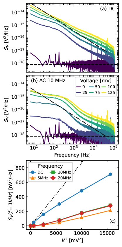
Fig. 2 shows the results of the low bias measurements. The effect of a DC bias on the junction is reported as noise spectra in Fig. 2 (a) for several values of the bias, from 0 to 10mV. The spectrum in the absence of bias is white, as expected for thermal noise. There is no sign of noise coming from the detection setup. The presence of a DC bias leads to an increase of noise at low frequency. The shape of the DC spectra appears more complex than a simple power law. At frequencies below Hz the noise spectral density decays slower than (the dashed-dotted line in 2 (a) indicates slope). From Hz to Hz, decays with a slope close to until it reaches the thermal noise. The noise reported here is always much greater than the shot/thermal noise of the junction which corresponds to 0.9nV.
In order to quantify the bias dependence of this noise we plot in Fig. 2 (c) the value of the noise spectral density measured at 1kHz, averaged over the bandwidth 0.9-1.1 kHz minus its value at equilibrium, as a function of . We clearly observe a linear dependence, in agreement with Eq.1 derived from the idea that the noise we observe comes from the fluctuations of the resistance of the tunnel junction. We decided to plot as a function of the DC voltage and not the DC current as in Eq.(1), but since the sample is almost perfectly linear, the conclusion is the same, only units change.
It is usual to characterize the amount of noise by the Hooge parameter [7, 8]. In tunnel junctions the resistance of the sample is inversely proportional to the area of the junction, so the noise spectral density takes the form [9]:
| (3) |
Taking the value of measured at 1kHz, the dotted line of Fig.2(c) corresponds to . Table I of [9] reports Hooge parameters of magnetic junctions using as insulating barrier to lie in the range 20 to 20000 . In comparison, our junction can be considered quiet. However, the Hooge parameter is known to increase with the resistance-area (RA) product in magnetic tunnel junctions[10, 11, 12]. This number is a measure of the inverse transparency of the barrier. The RA product of our sample is 4.16 km2, i.e. one order of magnitude below the smallest RA presented in [9]. The comparatively high transparency of our junction may explain its relatively small Hooge parameter.
We now discuss the effect of a pure AC bias on the sample. We show in Fig. 2 (b) noise spectra for various AC voltages at an excitation frequency of MHz. In strong contrast with the results for DC bias, the AC bias has no effect on the noise spectra. Comparison between DC and AC biases are summarized in Fig. 2 (c). AC bias has no effect for biases up to 10mV RMS and for all excitation frequencies, 5, 10 or 20 MHz. These results are in full agreement with the expectations of Eq.(2) based on the picture of resistance fluctuations. Indeed, from Eqs.(2) and (3), and the Hooge parameter mentioned above we expect a contribution of the noise to be below /Hz for an AC voltage of 10mV at 10 MHz.
III-B High voltage bias
We now explore the effect of DC and AC biases of higher amplitude, up to 125mV. The measurements are identical to those of the previous section, only the amplitude of the biases have increased. They are shown in Fig. 3.
Noise spectra for high DC biases are presented in Fig. 3(a). The shape of the DC spectra starts off similar to the low bias DC spectra, and become straighter as the bias increases. The spectrum at the highest DC bias is nearly a pure power law with a slope slightly less steep than than pure 1/f.
Noise spectra for an AC bias at 10 MHz are reported in Fig. 3(b). There is a clear effect of the AC excitation, in strong contrast to what happens with low AC bias.
The mean measured noise in the 900-1100 Hz bandwidth is shown for different bias values in Fig. 3(c). Again, the values of Fig. 3 (c) have had the thermal noise and shot noise subtracted and thus show only the excess noise. The case of DC bias is shown as blue circles. The data clearly fall below the law observed at low bias and indicated by a black dotted line: no longer scales as for high bias. The noise increases for AC bias: an AC excitation of 125mV RMS generates approximately a third of the noise generated by a 125mV DC voltage. There is also a small frequency dependence, the 5MHz excitation being slightly less effective than the 10 or 20MHz ones.
The fact that does not scale as for DC bias and that is influenced by the AC bias are in strong disagreement with the idea that the noise is due to resistance fluctuations that do not depend on the bias. As far as we know there is no theoretical explanation for this behaviour. A possible cause could be the nonlinearity of the characteristics of the junctions, although it deviates only very slightly from perfect linearity. It could also be that the resistance noise depends on the bias.
IV Conclusion
We have measured the effect of DC and AC bias on the low frequency noise appearing in metallic tunnel junctions. Our result are in contradiction with the simple picture that low frequency noise is due to resistance fluctuations that do not depend on voltage. This should help shed light on the mechanism responsible for the -like noise in these samples. Our experiment can be applied to many conducting samples that exhibit flicker noise to see if the behaviour we observe is general or not.
V Acknowledgments
We thank A. Horik and D. Grebe for their participation in the early stage of the experiment, G. Laliberté, E. Pinsolle and C. Lupien for their help with the experimental techniques, and A.-M. Tremblay for fruitful discussions. We thank Quantum e-Motion for providing us with the samples and for financial support. This work was supported by the Canada Research Chair program, the NSERC, the Canada First Research Excellence Fund, the FRQNT, and the Canada Foundation for Innovation.
References
- [1] M. Buckingham, Noise in Electronic Devices and Systems. Electrical and Electronic Engineering Series, E. Horwood, 1983.
- [2] A. Van der Ziel, Noise in Solid State Devices and Circuits. Wiley, 1986.
- [3] P. Dutta and P. M. Horn, “Low-frequency fluctuations in solids: noise,” Rev. Mod. Phys., vol. 53, pp. 497–516, Jul 1981.
- [4] C. T. Rogers and R. A. Buhrman, “Composition of noise in metal-insulator-metal tunnel junctions,” Phys. Rev. Lett., vol. 53, pp. 1272–1275, Sep 1984.
- [5] J. B. Johnson, “Thermal agitation of electricity in conductors,” Phys. Rev., vol. 32, pp. 97–109, Jul 1928.
- [6] H. Nyquist, “Thermal agitation of electric charge in conductors,” Phys. Rev., vol. 32, pp. 110–113, Jul 1928.
- [7] F. Hooge, “1/f noise is no surface effect,” Physics Letters A, vol. 29, no. 3, pp. 139–140, 1969.
- [8] F. Hooge, “1/f noise,” Physica B+C, vol. 83, no. 1, pp. 14–23, 1976.
- [9] Z. Q. Lei, G. J. Li, W. F. Egelhoff, P. T. Lai, and P. W. T. Pong, “Review of noise sources in magnetic tunnel junction sensors,” IEEE Transactions on Magnetics, vol. 47, no. 3, pp. 602–612, 2011.
- [10] A. F. Md Nor, T. Kato, S. J. Ahn, T. Daibou, K. Ono, M. Oogane, Y. Ando, and T. Miyazaki, “Low-frequency noise in MgO magnetic tunnel junctions,” Journal of Applied Physics, vol. 99, p. 08T306, 04 2006.
- [11] W. K. Park, J. S. Moodera, J. Taylor, M. Tondra, J. M. Daughton, A. Thomas, and H. Brückl, “Noise properties of magnetic and nonmagnetic tunnel junctions,” Journal of Applied Physics, vol. 93, pp. 7020–7022, 05 2003.
- [12] A. Gokce, E. R. Nowak, S. H. Yang, and S. S. P. Parkin, “1/f noise in magnetic tunnel junctions with MgO tunnel barriers,” Journal of Applied Physics, vol. 99, p. 08A906, 04 2006.