Engineering a High Spin Chern-Number Insulator in Epitaxial Sb Monolayer
Abstract
High spin Chern-number insulator (HSCI) emerges as a novel 2D topological phase of condensed matter that is beyond the classification scheme of topological quantum chemistry. In this work, we report the observation of a semimetallic Sb monolayer (-antimonene) with the same band topology as HSCI. Our first-principles calculations further indicate a moderate lattice strain can make Sb monolayer an insulator while retaining the nontrivial topological order. A quantized spin Hall conductivity is found in the HSCI phase of Sb monolayer. The results suggest strained Sb monolayer as a promising platform for exploring intriguing physical properties of the exotic HSCI topological matter.
pacs:
I Introduction
Topological phases of condensed matter are of significant interest for their novel electronic properties and device applications [1, 2, 3, 4]. Most topological materials can be classified in the framework of topological quantum chemistry (TQC) using symmetries and symmetry indicators (SI) at high-symmetry points (HSP)[5, 6]. Typically, band inversions occur at HSPs and serve to understand the non-trivial bulk topology. Recently, high spin Chern-number insulator (HSCI) has emerged as a novel topological phase that is beyond the description of TQC. In HSCIs, band inversion occurs at an even number of non-HSP momenta, leading to a zero topological invariant. Thus, this 2D system with time-reversal symmetry is regarded as topologically trivial according to the TQC classification. On the other hand, it has theoretically demonstrated that in the phase of Sb and Bi monolayers [7, 8], a nontrivial distribution of Berry curvature around the momenta where band inversion occurs gives rise to a high spin Chern number =2. Consequently, the HSCI system harbors two pairs of gapless helical edge states, which can drive a larger spin-polarized current. It has also been proven that this new type of bulk-boundary correspondence in HSCI is robust even in the presence of spin-orbit coupling (SOC) due to the protection of a “hidden” feature spectrum topology [9]. Therefore, there is a pressing need for the realization of an experimental viable HSCI to enable the study of exotic behaviors of this unconventional topological matter.
In this work, we synthesized -Sb monolayer on SnSe substrate by molecular beam epitaxy (MBE). Our angle-resolved photoemission (ARPES) measurements and first-principles calculations indicate that the nearly freestanding -Sb monolayer on SnSe, though semimetallic without a global band gap, shares the same band topology as HSCI. Our calculations further show that a moderate uniaxial lattice strain (2% in the zigzag direction) can make -Sb an insulator while retaining the nontrivial HSCI band topology. The desired lattice strains can be achieved by choosing appropriate substrates for the MBE synthesis, for ultrathin epitaxial films are particularly susceptible to substrate effects. A comprehensive phase diagram of -Sb under strains is provided as a guide for future experimental investigation of the exotic HSCI phase with desired electronic properties.
II Results and Discussion
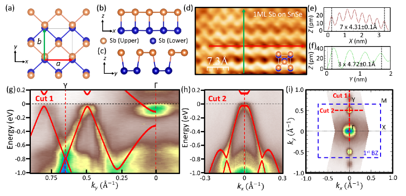
Sb monolayer in phase has a black phosphorous (BP) crystal structure with the space group as shown Figs. 1(a-b). There are two atomic sublayers with a vertical spacing of 2.79 . -Sb monolayer was grown by MBE on a cleaved (001)-surface of SnSe. Atomic-resolution STM image taken from the MBE sample reveals the BP structure of 1ML -Sb (Fig. 1(d)), with averaged lattice constants of = 4.31 0.1 (Fig. 1(e)) and = 4.72 0.1 (Fig. 1(f)). Fully relaxed crystal structure of 1ML -Sb based on first-principles calculations shows in-plane lattice constants of = 4.29 and = 4.77 , indicating our MBE sample is close to being freestanding. The nearly freestanding nature is also expected for the weak coupling between -Sb and the semiconducting vdW surface of SnSe [10].
The band structure of the MBE-grown 1ML -Sb was mapped out by ARPES (Figs. 1(g-i)). The measured Fermi surface (Fig. 1(i)) shows three prominent features near the Fermi level, namely, an electron pocket from the conduction band at and two hole pockets centered at from the valence band. The spectrum along the high-symmetry direction Y is plotted in Fig. 1(g). The overlaid red solid curves are the first-principles band dispersion based on experimental lattice parameters. The good agreement between the ARPES spectrum and the calculated bands indicates the system is semimetallic with a small negative gap between the conduction and valence bands. An ARPES spectral cut taken along the line “Cut2” at perpendicular to Y (Fig. 1(h)) shows the hole-like band barely touches the Fermi level and is separated from the conduction band by a small energy gap of 0.15 eV. The band dispersion resembles a gaped conical surface. The conical hole pockets at are referred to as two valleys in the following discussions.
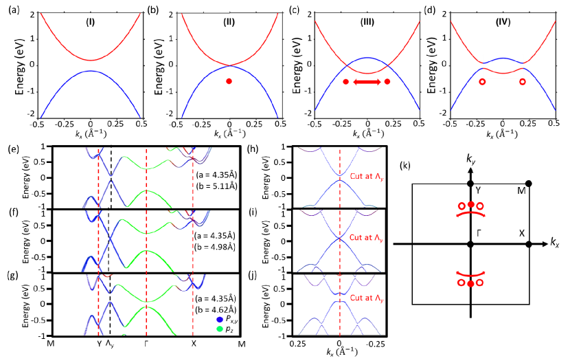
Now we discuss the band topology of 1ML -Sb. The nontrivial high spin Chern number is generated by the band inversion at the two valleys of 1ML -Sb. A schematic of this process is shown in Figs. 2(a-d). Starting from a conventional semiconducting band structure in the absence of SOC (Fig. 2(a)). The band gap can be completely closed by continuously tuning a parameter of the system such as lattice constants, resulting in a 2D Dirac nodal point (Fig. 2(b)). Further tuning the parameter causes a band inversion between the conduction and valence bands and generates two Dirac points (DPs) marked by red dots in Fig. 2(c). (We note that the DPs generated this way are located at generic momenta rather than HSPs. Those DPs are referred to in the literature as “unpinned” Dirac states [11, 12].) The inclusion of the spin-orbit coupling gaps out the unpinned Dirac states (Fig. 2(d)) and induces a nontrivial Berry curvature around the DPs. This process of band inversion can be seen in the band dispersion of 1ML -Sb with varied lattice parameters around the valley momenta (0,). Figures 2(e-g) shows the calculated band structure of 1ML -Sb with lattice constants , , respectively. The bands near the valley momentum primarily originate from the orbitals of Sb atoms. The energy gap at the valley closes and reopens as decreases from 5.11Åto 4.62Å. The gap vanishes at the critical lattice values of (4.35Å, 4.98Å). Figures 2(h-j) demonstrate the valley band dispersion calculated along the line perpendicular to with lattice parameters corresponding to those in Figs. 2(e-g). The Mexican-hat-like band dispersion near the conduction band bottom in Fig. 2(j) indicates the SOC-induced band gap (as shown in Fig 2(d)) and an inverted order between the conduction and valence bands at the valley momentum (0, ). The band inversion induced by varying lattice parameters is schematically plotted in the 1st Brillouin zone of 1ML -Sb in Fig. 2(k). It is obvious that the band inversion occurs at both valleys at (0, ), giving rise to a high spin Chern number =2. The 1ML -Sb with inverted band order at its two valleys possesses two pairs of gapless spin-polarized edge states. This new type of bulk-boundary correspondence is guaranteed by a “hidden” feature spectrum topology as reported in the previous work[9]. On the other hand, the double band inversion at generic momenta gives a trivial topological invariant, thus indicating the 1ML -Sb in the HSCI phase is a new type of topological materials beyond the classification of TQC.
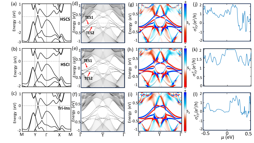
To demonstrate the nontrivial band topology and protected helical edge states, we calculated the edge state bands and spin Hall conductance of 1ML -Sb. The results are summarized in Fig. 3. The band structure and projected edge state spectrum of 1ML -Sb based our experimental lattice constants, and are plotted in Figs. 3(a,d). The calculated band structure is in good agreement with our ARPES result (Fig. 1(g)), indicating a semimetallic nature of the nearly freestanding -Sb monolayer grown by MBE. Nevertheless, the spin Chern number can be defined for the semimetallic -Sb monolayer for a continuous band gap separating the conduction and valence bands through the whole Brillouin zone. It turns out that the spin Chern number of the valence band is the same as that of the HSCI phase. In this sense, the freestanding -Sb monolayer can be regarded as a high spin Chern-number semimetal (HSCS). The nontrivial band topology can be seen in the edge state spectrum calculated for a semi-infinite slab along the armchair direction (which corresponds to the direction in the edge Brillouin zone). There are two pairs of topological edge state (TES) bands (marked by “TES1” and “TES2” in Fig. 3(d)) traversing the energy gap between the conduction and valence bands. Both TES bands possess a helical spin texture as shown in Fig. 3(g). For practical applications of spin-polarized TESs arising from the bulk boundary correspondence in topological systems [13, 14, 15, 16, 17, 18, 19], it is desirable to generate a global band gap between the conduction and valence bands. We calculated the bulk and edge bands of 1ML -Sb with a 3% uniaxial tensile strain in x direction, and the results are shown in Figs. 3(b,e,h,k). The tensile strain in x direction moves the electron pocket at up to above the Fermi level and leads to a global band gap. No band inversion happens in the process of tuning up the tensile strain from 0% to 3%, indicating the freestanding monolayer and this strained one share the same band topology. Two pairs of helical TES bands are found in the calculated edge state spectrum of the strained monolayer. Moreover, a plateau of value shows up in the calculated spin Hall conductance curves at chemical potential () values within the energy gap of the strained monolayer (Fig. 3(k)). The quantized spin Hall conductance is due to the lattice symmetry and the feature spectrum topology[7, 9]. By contrast, a topologically trivial insulator (Tri-Ins) can be generated by applying a uniaxial tensile strain in y direction. Figures 3(c,f,i) show the band structure and edge state spectrum of -Sb monolayer with a 4% uniaxial tensile strain in y direction. The bulk band structure is with a global band gap. However, no edge state band in this case traverses the bulk band gap, indicating the trivial band topology. The spin Hall conductance of -Sb monolayer in the trivial insulating phase is nearly zero for the chemical potential within the band gap. In the HSCS phase of freestanding -Sb monolayer, the spin Hall conductance is nonzero near the Fermi level, but not quantized due to the presence of bulk band pockets at the Fermi level.
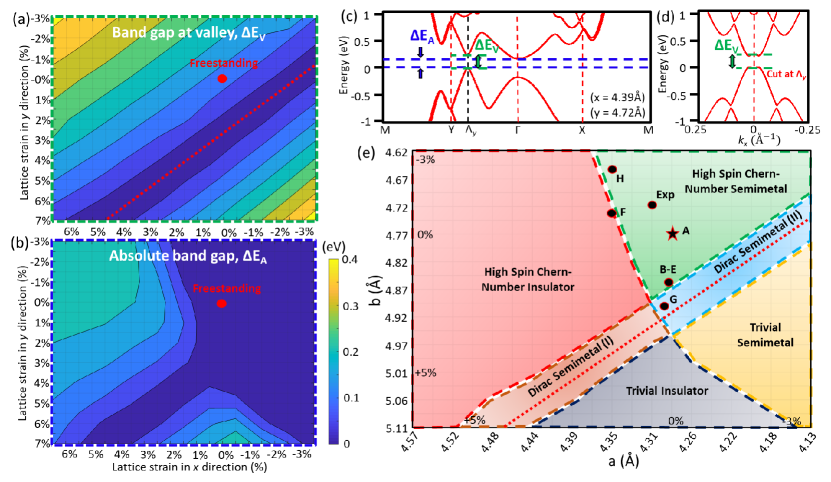
Topologically distinct insulating phases of -Sb monolayer can be achieved by applying moderate lattice strains. To understand the influence of lattice strains on the band topology of -Sb monolayer, we performed systematic simulations of the band structure with tensile (positive) and compressive (negative) strains in x and y directions. The results are shown in Fig. 4. In particular, we extracted the absolute values of the global band gap, between the conduction and valence bands and the band gap at the valleys, as defined in Figs. 4(c,d). A nonzero means the system is an insulator/semiconductor. A vanishing corresponds to a gapless Dirac cone at the valleys, and the system is at the critical point proximal to two topologically distinct phases. The maps of and under different lattice strains in x and y directions are plotted in Figs. 4(a) and 4(b), respectively. The red dot marks the lattice of freestanding -Sb monolayer. The red dashed line with in Fig. 4(a) is the boundary between the nontrivial HSCI/HSCS and the trivial insulator/semimetal phases. Combining the results from Figs. 4(a,b), we can get the phase diagram of -Sb monolayer under strains (Fig. 4(e)), which allows simple identification of the band properties of the strained films. For example, both freestanding monolayer (marked by the star in Fig. 4(e)) and our MBE-grown sample (labeled with “Exp”) lie in the region of “high spin Chern-number semimetal”, and a moderate tensile strain of 2̃% in x direction can make them an HSCI topological insulator. The lattice parameter values of -Sb monolayer extracted from previous works [20, 21, 22, 23, 24, 8, 25, 26] are marked in the phase diagram. The lattice of epitaxial monolayer is susceptible to substrate effects, such as charge transfer and interfacial coupling, underscoring the importance of substrate selection in engineering desired electronic properties.
In conclusion, our ARPES and first-principles results demonstrated that the epitaxial -Sb monolayer grown on SnSe substrate is a high spin Chern-number semimetal with the same band topology with the HSCI topological insulator. The comprehensive exploration of band topology of -Sb monolayers under strains sheds light on materials engineering of the novel HSCI topological phases in epitaxial atomic layers and offers a promising avenue for the development of novel electronic and spintronic devices based on the multiple spin-polarized edge channels.
III Methods
The -Sb thin films were grown on SnS and SnSe substrates in an integrated MBE-STM ultrahigh vacuum (UHV) system with base pressure below mbar. The SnSe were prepared by in-situ cleaving the surface and subsequent annealing to 250°C for 1 hour. Then, high-purity Sb (99.95%) was evaporated from a standard Knudsen cell. The deposition rate of Sb atoms was monitored by a quartz oscillator. The temperature of substrate was kept at 120°C during the growth.
The surface topography mapping was performed in situ by using the SPECS Aarhus-150 scanning tunneling microscopy (STM) system with a Tungsten tip at room temperature. After STM, the film was transferred in situ to the ARPES stage. ARPES measurements were performed at liquid nitrogen temperatures (109 K) using a SPECS PHOIBOS-150 hemisphere analyzer with a SPECS UVS 300 helium discharge lamp (He I = 21.2 eV). The energy resolution is 40 meV at 109 K.
References
- Hasan and Kane [2010] M. Z. Hasan and C. L. Kane, Rev. Mod. Phys. 82, 3045 (2010).
- Qi and Zhang [2011] X.-L. Qi and S.-C. Zhang, Rev. Mod. Phys. 83, 1057 (2011).
- Bansil et al. [2016] A. Bansil, H. Lin, and T. Das, Rev. Mod. Phys. 88, 021004 (2016).
- Xiao and Yan [2021] J. Xiao and B. Yan, Nature Reviews Physics 3, 283 (2021).
- Bradlyn et al. [2017] B. Bradlyn, L. Elcoro, J. Cano, M. G. Vergniory, Z. Wang, C. Felser, M. I. Aroyo, and B. A. Bernevig, Nature 547, 298 (2017).
- Tang et al. [2019] F. Tang, H. C. Po, A. Vishwanath, and X. Wan, Nature 566, 486 (2019).
- Wang et al. [2022] B. Wang, X. Zhou, Y.-C. Lin, H. Lin, and A. Bansil, (2022), arXiv:2202.04162 [cond-mat.mes-hall] .
- Bai et al. [2022] Y. Bai, L. Cai, N. Mao, R. Li, Y. Dai, B. Huang, and C. Niu, Phys. Rev. B 105, 195142 (2022).
- Baokai Wang and Lin [2023] X. Z. T. O. Baokai Wang, Yi-Chun Hung and H. Lin, (2023), arXiv:2310.14832 [cond-mat.mes-hall] .
- Lu et al. [2023] Q. Lu, P. V. S. Reddy, H. Jeon, A. R. Mazza, M. Brahlek, W. Wu, S. A. Yang, J. Cook, C. Conner, X. Zhang, A. Chakraborty, H.-J. Tien, C.-H. Tseng, P.-Y. Yang, S.-W. Lie, H. Lin, T.-C. Chiang, G. Vignale, A.-P. Li, T.-R. Chang, R. G. Moore, , and G. Bian, (2023), arXiv:2303.02971 [cond-mat.mes-hall] .
- Lu et al. [2016] Y. Lu, D. Zhou, G. Chang, S. Guan, W. Chen, Y. Jiang, J. Jiang, X.-s. Wang, S. A. Yang, Y. P. Feng, Y. Kawazoe, and H. Lin, npj Computational Materials 2, 16011 (2016).
- Lu et al. [2022] Q. Lu, J. Cook, X. Zhang, K. Y. Chen, M. Snyder, D. T. Nguyen, P. V. S. Reddy, B. Qin, S. Zhan, L.-D. Zhao, P. J. Kowalczyk, S. A. Brown, T.-C. Chiang, S. A. Yang, T.-R. Chang, and G. Bian, Nature Communications 13, 4603 (2022).
- Schnyder et al. [2008] A. P. Schnyder, S. Ryu, A. Furusaki, and A. W. W. Ludwig, Phys. Rev. B 78, 195125 (2008).
- Mong and Shivamoggi [2011] R. S. K. Mong and V. Shivamoggi, Phys. Rev. B 83, 125109 (2011).
- Graf and Porta [2013] G. M. Graf and M. Porta, Communications in Mathematical Physics 324, 851 (2013).
- Sedlmayr et al. [2017] N. Sedlmayr, V. Kaladzhyan, C. Dutreix, and C. Bena, Phys. Rev. B 96, 184516 (2017).
- Hatsugai [2009] Y. Hatsugai, Solid State Communications 149, 1061 (2009), recent Progress in Graphene Studies.
- Rhim et al. [2018] J.-W. Rhim, J. H. Bardarson, and R.-J. Slager, Phys. Rev. B 97, 115143 (2018).
- Li and Haldane [2008] H. Li and F. D. M. Haldane, Phys. Rev. Lett. 101, 010504 (2008).
- Shi et al. [2020] Z.-Q. Shi, H. Li, C.-L. Xue, Q.-Q. Yuan, Y.-Y. Lv, Y.-J. Xu, Z.-Y. Jia, L. Gao, Y. Chen, W. Zhu, and S.-C. Li, Nano Letters 20, 8408 (2020), pMID: 33064495, https://doi.org/10.1021/acs.nanolett.0c03704 .
- Salehitaleghani et al. [2023] S. Salehitaleghani, T. Maerkl, P. J. Kowalczyk, X. Wang, G. Bian, T.-C. Chiang, and S. A. Brown, Applied Surface Science 635, 157674 (2023).
- Märkl et al. [2017] T. Märkl, P. J. Kowalczyk, M. L. Ster, I. V. Mahajan, H. Pirie, Z. Ahmed, G. Bian, X. Wang, T.-C. Chiang, and S. A. Brown, 2D Materials 5, 011002 (2017).
- Shi et al. [2019] Z.-Q. Shi, H. Li, Q.-Q. Yuan, Y.-H. Song, Y.-Y. Lv, W. Shi, Z.-Y. Jia, L. Gao, Y.-B. Chen, W. Zhu, and S.-C. Li, Advanced Materials 31, 1806130 (2019), https://onlinelibrary.wiley.com/doi/pdf/10.1002/adma.201806130 .
- Li et al. [2022] J. Li, K. Yu, X. Zhang, Y. Li, L. Qiao, X. Peng, X. Dong, Z. Wang, J. Ma, W. Xiao, and Y. Yao, The Journal of Physical Chemistry C 126, 5022 (2022), https://doi.org/10.1021/acs.jpcc.1c10177 .
- Niu et al. [2021] Y.-Y. Niu, C.-R. Wang, Q.-Q. Yuan, C.-L. Xue, L.-G. Dou, Y.-Y. Lv, Y. Chen, and S.-C. Li, AIP Advances 11, 095014 (2021), https://pubs.aip.org/aip/adv/article-pdf/doi/10.1063/5.0061987/12828722/095014_1_online.pdf .
- Lu et al. [2021] Q. Lu, K. Y. Chen, M. Snyder, J. Cook, D. T. Nguyen, P. V. S. Reddy, T.-R. Chang, S. A. Yang, and G. Bian, Phys. Rev. B 104, L201105 (2021).