In-situ tuning of optomechanical crystals with nano-oxidation
Abstract
Optomechanical crystals are a promising device platform for quantum transduction and sensing. Precise targeting of the optical and acoustic resonance frequencies of these devices is crucial for future advances on these fronts. However, fabrication disorder in these wavelength-scale nanoscale devices typically leads to inhomogeneous resonance frequencies. Here we achieve in-situ, selective frequency tuning of optical and acoustic resonances in silicon optomechanical crystals via electric field-induced nano-oxidation using an atomic-force microscope. Our method can achieve a tuning range nm () for the optical resonance wavelength in the telecom C-band, and MHz () for the acoustic resonance frequency at GHz. The tuning resolution of pm for the optical wavelength, and kHz for the acoustic frequency allows us to spectrally align multiple optomechanical crystal resonators using optimal oxidation patterns determined via an inverse design protocol. Our results establish a method for precise post-fabrication tuning of optomechancical crystals. This technique can enable coupled optomechanical resonator arrays, scalable resonant optomechanical circuits, and frequency matching of microwave-optical quantum transducers.
1 Introduction
Optomechanical crystals (OMCs) provide a coherent interface between optical photons and acoustic phonons [1]. This capability is now being utilized in microwave-optical quantum transducers [2, 3, 4, 5, 6] towards connecting gigahertz frequency superconducting quantum processors [7] via low-loss optical communication channels. In parallel efforts, OMCs have enabled coherent control and routing of phonons in chip-scale optomechanical circuits [8, 9, 10] with demonstrations of nonreciprocal optical transmission [11] and topologically protected phonon transport [12]. However, scaling to multi-node quantum networks and more complex optomechanical circuits is challenging due to variations in optical and acoustic resonance frequencies across devices caused by fabrication imperfections. In particular, since critical feature sizes in OMCs are affected by the precision limits of electron beam lithography and reactive ion etching, the spread in resonance frequencies across devices can be more than a hundred times the resonance linewidths, thereby hindering frequency alignment.
Post-fabrication tuning of optical resonance frequencies in chip-scale microcavities has been achieved using a variety of techniques including laser-assisted thermal oxidation [13], atomic force microscope (AFM) nano-oxidation [14, 15], strain tuning [16, 17], thermo-optic tuning [18, 19], and gas condensation [20, 21]. However, since OMCs co-localize optical and acoustic resonances in a wavelength-scale volume, selective tuning of both optical and acoustic resonances without compromising the quality factors of either is a significantly more complex endeavor and an outstanding technical challenge. Here we use AFM nano-oxidation tuning to demonstrate such control over the resonance frequencies of OMCs. In our approach, field-induced oxidation of the silicon device surface with high spatial resolution allows us to tune the acoustic resonance by modifying the local mass distribution and elasticity, and the optical resonance by modifying the local refractive index. By using an inverse design protocol to guide the nano-oxidation sequence in real-time, we achieve simultaneous alignment of the optical and acoustic resonance frequencies of multiple OMC cavities.
2 AFM nano-oxidation setup
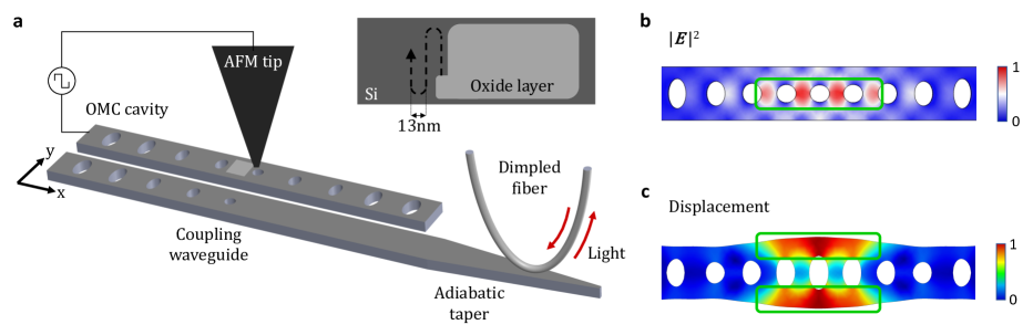
A simplified schematic of the experimental setup is shown in Fig. 1a. We perform nano-oxidation using a conductive chromium/platinum coated silicon AFM tip with a radius <25 nm [22], and track the optical and acoustic resonances in real-time by performing optomechanical spectroscopy via a dimpled optical fiber coupled to the device. The AFM is operated in tapping mode while a voltage bias is applied to the conductive tip, and the silicon-on-insulator (SOI) chip with a silicon device layer resistivity of 5 k-cm is grounded. When the voltage-biased AFM tip is brought close to the silicon surface, a strong electric field triggers an electrochemical reaction between ions in the native water meniscus and the silicon surface, resulting in local oxidation of silicon. Importantly, this reaction can proceed even when the silicon surface is covered with native oxide, because the strong local electric field allows oxyanions (OH- , O-) to diffuse through the native oxide [23]. In our experiments, we maintain the AFM setup enclosure at ambient conditions with a relative humidity of 405 and temperature of 231∘C, and apply a square wave voltage oscillating between V at a frequency of 20 Hz to the AFM tip.
The OMC cavities in this work were fabricated on an SOI chip with a nm thick silicon device layer. The cavities were patterned via electron beam lithography followed by reactive ion etching, and finally suspended by removing the buried oxide layer with an anhydrous vapor hydrofluoric acid etch. The devices were designed to support a fundamental TE-like optical resonance at a wavelength of 1550 nm and a breathing acoustic resonance at a frequency of 5.1 GHz (Fig. 1b,c) [24]. An on-chip adiabatic waveguide coupler [25] allows for optical coupling to the OMC cavity using a dimpled optical fiber. The optical spectrum of the OMC cavity was probed in reflection mode, and the resonance frequencies were recorded before and after each step of the nano-oxidation sequence. To measure the acoustic spectrum of the device, we routed the optical signal reflected from the device to a high-speed photodetector and measured the power spectral density (PSD) of the photodetector electrical output on a spectrum analyzer. The result is proportional to the PSD of thermal displacement fluctuations of the acoustic mode which are transduced onto the optical signal via the optomechanical interaction in the device. In these measurements, the laser was blue-detuned with respect to the optical resonance frequency by a detuning close to the acoustic resonance frequency, and operated at low power to minimize optomechanical back-action on the acoustic mode [26].
3 Nano-oxidation characterization
From the simulated mode profiles shown in Fig. 1b,c, we identified two strategic oxidation regions for selective tuning of the optical and acoustic modes. Nano-oxidation in the region shown with the green rectangle in Fig. 1b is expected to induce a relatively large change in the optical resonance due to a high concentration of electric field energy. Here the impact on the acoustic resonance is expected to be minimal due to two reasons. First, the displacement amplitude is small in this region. Second, even though the stress amplitude is large in this region, the Young’s modulus of the oxide layer when weighted by its thickness is similar to that of the original silicon. In contrast, nano-oxdiation on the regions shown with the green rectangles in Fig. 1c leads to a large acoustic resonance shift and a small optical wavelength shift due to the high concentration of motional mass and low concentration of electric field energy. In section 5.4 of the supplementary information, we show the results of finite element method (FEM) simulations where we investigated the optical and acoustic frequency shifts due to creation of an oxide pixel at an arbitrary location on the OMC surface. This allowed us to identify candidate regions for fine tuning of optical and acoustic resonance frequencies with maximal selectivity. For coarse frequency tuning, we opted to use larger, rectangular oxide patterns instead of oxide pixels to maximize the tuning range at the expense of selectivity.
Prior to experiments on OMC devices, we characterized the effect of the AFM tapping amplitude and scanning velocity on nano-oxidation using a bare silicon chip. We observed that lower tapping amplitude and slower scanning velocities result in wider and thicker oxide lines. We measured the three-dimensional profiles of field-induced oxide lines and pixels using AFM measurements as described in section 5.2 of the supplementary information. Based on the amount of frequency tuning required, we operated the AFM in two distinct modes which we refer to as ‘mild’ and ‘aggressive’ tuning modes. In the mild tuning mode, the tapping amplitude and scan speed were set to 15 nm and 100 nm/s, respectively, resulting in oxide thickness of approximately 1.2 nm. In the aggressive tuning mode, the tapping amplitude and scan speed were set to 5 nm and 50 nm/s, respectively, leading to oxide thickness of approximately 2.5 nm. In the mild tuning mode, nano-oxidation was found to generate single pixels with a lateral size of approximately 25 nm. In order to obtain thicker and more uniform oxide patterns with a raster scan, we used a line spacing of 13 nm with significant overlap between neighboring lines as illustrated in the inset of Fig. 1a. This procedure allowed us to generate oxide layers with a thickness of 1.6 nm and 3.2 nm in the mild and aggressive tuning modes, respectively.
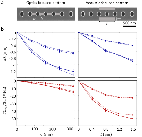
After establishing these nano-oxidation parameters, we performed optical and acoustic resonance frequency tuning experiments on a single OMC cavity. We specifically studied the impact of two oxidation patterns: (i) an optics-focused pattern (Fig. 2a left) composed of four rectangles located between the five central ellipses in the beam; here the lengths of the rectangles were kept constant at = 170 nm, while their width, was varied, and (ii) an acoustics-focused pattern (Fig. 2a, right) composed of two rectangles situated at the edge of the OMC cavity; here the widths of the rectangles were kept fixed at 120 nm, while their length, was varied. As shown in Fig. 2b, the experimentally measured tuning of the resonance frequencies (solid and dashed lines) agrees with simulation results (dotted lines). For the optics-focused pattern, increasing leads to a large reduction in the optical wavelength and a smaller reduction in acoustic frequency. For the acoustics-focused pattern, increasing leads to a decrease in acoustic frequency due to increasing motional mass () and a decrease in the optical wavelength due to a decrease in the effective dielectric constant. Aggressive oxidation at 320 nm resulted in more than 1.2 nm blue shift of the optical wavelength while aggressive oxidation at = 1.6 m resulted in more than 50 MHz reduction in the acoustic frequency. In Fig. 2b, each data point represents the average value and the standard deviation obtained from five devices. For each device, the patterns were applied cumulatively, starting from the center and adding more oxide to increase either or at each step.
4 Simultaneous optical and acoustic frequency tuning
To achieve simultaneous tuning of optical and acoustic resonances, we define a joint pattern consisting of a union of the previously introduced optics-focused and acoustics-focused patterns. This is parameterized by geometric parameters and , and binary variables () which denote mild or aggressive oxidation in the optical (acoustic) components of the joint pattern. Using the experimental data shown in Fig. 2, we interpolate and as a function of the parameters . To achieve the desired frequency shifts, we developed an inverse design algorithm to find an optimal combination of the acoustic and optics focused patterns. The algorithm takes the desired frequency and wavelength shift as the input and generates the required joint oxidation pattern by searching for the most suitable combination of and . The algorithm starts the search from milder oxidation modes to prevent a reduction in optical Q-factor as explained in supplementary section 5.5.
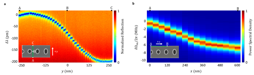
While the inverse design algorithm is sufficient for coarse tuning of the OMC wavelength and frequency, fine frequency alignment to within the linewidth of the optical and acoustic resonances requires pixel-by-pixel nano-oxidation with real-time feedback. This method allows for 1 pm precision for optical wavelength tuning and 150 kHz precision for acoustic resonance tuning. To quantify the sensitivity of the optical resonance wavelength to single oxide pixels, we applied a pixel-by-pixel linear oxide pattern perpendicular to the OMC long axis with a pitch of 13 nm shown in the inset of Fig 3a. The resonance spectra recorded in Fig. 3a for each incremental pixel in the oxidation sequence reveal a decrease in the per-pixel wavelength shift towards the edges of the OMC, with an observed shift of 1.1 pm/px at the extreme points A and C. This spatial dependence is in agreement with predictions from FEM simulations, as discussed in supplementary section 5.4. We perform a similar sensitivity analysis for the acoustic resonance via a pixel-by-pixel linear oxide pattern applied with a pitch of 40 nm along the edge of the OMC, shown in the inset of Fig 3b. The acoustic resonance spectrum is recorded after the addition of every oxide pixel, and the results are shown in Fig. 3b. We measure a maximum frequency shift of -1 MHz/px at point A which is in line with the center of the OMC cavity. As we move away from the center, the sensitivity eventually decreases to a value of -150 kHz/px as measured at the extreme point B.
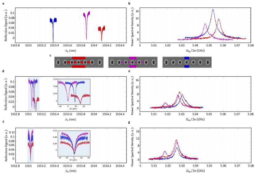
After characterizing coarse and fine tuning of optical and acoustic resonance frequencies of a single OMC cavity, we used these techniques to perform frequency alignment of both the optical and acoustic resonances of three OMC cavities. Due to constraints on the maximum achievable tuning range, we pre-select cavities with initial optical wavelength spread <1 nm and acoustic frequency spread <20 MHz, shown on Fig. 4a, b. We begin with coarse tuning steps using oxidation patterns generated by the inverse design algorithm as shown in Fig. 4c. This aligns the optical resonance wavelengths across all cavities to within a tolerance of <200 pm and acoustic resonance frequencies to withina tolerance of 5 MHz. The results of the coarse tuning are shown on Fig. 4d,e. We then proceed to real-time, pixel-by-pixel oxidation with feedback to achieve fine tuning of the resonance frequencies. After four rounds of fine-tuning, the optical and acoustic resonance frequencies were successfully tuned to within 2 pm and 500 kHz respectively (see Fig 4f, g). A step-by-step description of the frequency alignment procedure is described in detail in supplementary section 5.6.
5 Outlook
We have shown simultaneous, real-time tuning of optical and acoustic resonances in OMC cavities via AFM nano-oxidation, demonstrating optical wavelength and acoustic frequency shifts >2 nm (0.13%) and >60 MHz (1.2%), respectively. Such in-situ tuning methods could enable the realization of coupled optomechanical resonator arrays to study topological phases of photons and phonons [27, 28, 29, 12]. In the context of OMC-based microwave-optical quantum transducers [2, 3, 4, 5, 6], the nano-oxidation tuning demonstrated here will enable post-fabrication frequency alignment of transducers in multiple nodes of a quantum network. Moreover, these techniques are applicable to other material systems such as silicon nitride [30], where tuning of optomechanical devices may be required [31]. Finally, AFM nano-oxidation could be a valuable technique for fundamental studies of two-level systems (TLS) in amorphous materials [32] by enabling spatially targeted creation of TLS in acoustic [1] and superconducting [33] devices.
References
- [1] G. S. MacCabe, H. Ren, J. Luo, J. D. Cohen, H. Zhou, A. Sipahigil, M. Mirhosseini, and O. Painter, “Nano-acoustic resonator with ultralong phonon lifetime,” \JournalTitleScience 370, 840–843 (2020).
- [2] M. Mirhosseini, A. Sipahigil, M. Kalaee, and O. Painter, “Superconducting qubit to optical photon transduction,” \JournalTitleNature 588, 599–603 (2020).
- [3] S. Meesala, S. Wood, D. Lake, P. Chiappina, C. Zhong, A. D. Beyer, M. D. Shaw, L. Jiang, and O. Painter, “Non-classical microwave-optical photon pair generation with a chip-scale transducer,” \JournalTitlearXiv preprint arXiv:2303.17684 (2023).
- [4] W. Jiang, F. M. Mayor, S. Malik, R. Van Laer, T. P. McKenna, R. N. Patel, J. D. Witmer, and A. H. Safavi-Naeini, “Optically heralded microwave photon addition,” \JournalTitleNature Physics 19, 1423–1428 (2023).
- [5] M. J. Weaver, P. Duivestein, A. C. Bernasconi, S. Scharmer, M. Lemang, T. C. v. Thiel, F. Hijazi, B. Hensen, S. Gröblacher, and R. Stockill, “An integrated microwave-to-optics interface for scalable quantum computing,” \JournalTitleNature Nanotechnology pp. 1–7 (2023).
- [6] H. Zhao, A. Bozkurt, and M. Mirhosseini, “Electro-optic transduction in silicon via gigahertz-frequency nanomechanics,” \JournalTitleOptica 10, 790–796 (2023).
- [7] M. Kjaergaard, M. E. Schwartz, J. Braumüller, P. Krantz, J. I.-J. Wang, S. Gustavsson, and W. D. Oliver, “Superconducting qubits: Current state of play,” \JournalTitleAnnual Review of Condensed Matter Physics 11, 369–395 (2020).
- [8] K. Fang, M. H. Matheny, X. Luan, and O. Painter, “Optical transduction and routing of microwave phonons in cavity-optomechanical circuits,” \JournalTitleNature Photonics 10, 489–496 (2016).
- [9] R. N. Patel, Z. Wang, W. Jiang, C. J. Sarabalis, J. T. Hill, and A. H. Safavi-Naeini, “Single-mode phononic wire,” \JournalTitlePhys. Rev. Lett. 121, 040501 (2018).
- [10] A. Zivari, N. Fiaschi, R. Burgwal, E. Verhagen, R. Stockill, and S. Gröblacher, “On-chip distribution of quantum information using traveling phonons,” \JournalTitleScience Advances 8, eadd2811 (2022).
- [11] K. Fang, J. Luo, A. Metelmann, M. H. Matheny, F. Marquardt, A. A. Clerk, and O. Painter, “Generalized non-reciprocity in an optomechanical circuit via synthetic magnetism and reservoir engineering,” \JournalTitleNature Physics 13, 465–471 (2017).
- [12] H. Ren, T. Shah, H. Pfeifer, C. Brendel, V. Peano, F. Marquardt, and O. Painter, “Topological phonon transport in an optomechanical system,” \JournalTitleNature Communications 13, 3476 (2022).
- [13] C. L. Panuski, I. Christen, M. Minkov, C. J. Brabec, S. Trajtenberg-Mills, A. D. Griffiths, J. J. McKendry, G. L. Leake, D. J. Coleman, C. Tran et al., “A full degree-of-freedom spatiotemporal light modulator,” \JournalTitleNature Photonics 16, 834–842 (2022).
- [14] K. Hennessy, C. Högerle, E. Hu, A. Badolato, and A. Imamoğlu, “Tuning photonic nanocavities by atomic force microscope nano-oxidation,” \JournalTitleApplied physics letters 89, 041118 (2006).
- [15] A. Yokoo, T. Tanabe, E. Kuramochi, and M. Notomi, “Ultrahigh-q nanocavities written with a nanoprobe,” \JournalTitleNano letters 11, 3634–3642 (2011).
- [16] C. W. Wong, P. T. Rakich, S. G. Johnson, M. Qi, H. I. Smith, E. P. Ippen, L. C. Kimerling, Y. Jeon, G. Barbastathis, and S.-G. Kim, “Strain-tunable silicon photonic band gap microcavities in optical waveguides,” \JournalTitleApplied physics letters 84, 1242–1244 (2004).
- [17] I. Luxmoore, E. D. Ahmadi, B. Luxmoore, N. Wasley, A. Tartakovskii, M. Hugues, M. Skolnick, and A. Fox, “Restoring mode degeneracy in h1 photonic crystal cavities by uniaxial strain tuning,” \JournalTitleApplied Physics Letters 100, 121116 (2012).
- [18] M. S. Nawrocka, T. Liu, X. Wang, and R. R. Panepucci, “Tunable silicon microring resonator with wide free spectral range,” \JournalTitleApplied physics letters 89, 071110 (2006).
- [19] A. Faraon, D. Englund, I. Fushman, J. Vučković, N. Stoltz, and P. Petroff, “Local quantum dot tuning on photonic crystal chips,” \JournalTitleApplied Physics Letters 90, 213110 (2007).
- [20] S. Mosor, J. Hendrickson, B. Richards, J. Sweet, G. Khitrova, H. Gibbs, T. Yoshie, A. Scherer, O. Shchekin, and D. Deppe, “Scanning a photonic crystal slab nanocavity by condensation of xenon,” \JournalTitleApplied Physics Letters 87, 141105 (2005).
- [21] S. Strauf, M. T. Rakher, I. Carmeli, K. Hennessy, C. Meier, A. Badolato, M. J. DeDood, P. M. Petroff, E. L. Hu, E. Gwinn et al., “Frequency control of photonic crystal membrane resonators by monolayer deposition,” \JournalTitleApplied Physics Letters 88, 043116 (2006).
- [22] “Atomic force microscopy: Park systems,” .
- [23] R. Garcia, R. V. Martinez, and J. Martinez, “Nano-chemistry and scanning probe nanolithographies,” \JournalTitleChemical Society Reviews 35, 29–38 (2006).
- [24] J. Chan, A. H. Safavi-Naeini, J. T. Hill, S. Meenehan, and O. Painter, “Optimized optomechanical crystal cavity with acoustic radiation shield,” \JournalTitleApplied Physics Letters 101, 081115 (2012).
- [25] S. Gröblacher, J. T. Hill, A. H. Safavi-Naeini, J. Chan, and O. Painter, “Highly efficient coupling from an optical fiber to a nanoscale silicon optomechanical cavity,” \JournalTitleApplied Physics Letters 103, 181104 (2013).
- [26] M. Aspelmeyer, T. J. Kippenberg, and F. Marquardt, “Cavity optomechanics,” \JournalTitleReviews of Modern Physics 86, 1391 (2014).
- [27] V. Peano, C. Brendel, M. Schmidt, and F. Marquardt, “Topological phases of sound and light,” \JournalTitlePhysical Review X 5, 031011 (2015).
- [28] V. Peano, M. Houde, C. Brendel, F. Marquardt, and A. A. Clerk, “Topological phase transitions and chiral inelastic transport induced by the squeezing of light,” \JournalTitleNature communications 7, 1–8 (2016).
- [29] C. Brendel, V. Peano, O. J. Painter, and F. Marquardt, “Pseudomagnetic fields for sound at the nanoscale,” \JournalTitleProceedings of the National Academy of Sciences 114, E3390–E3395 (2017).
- [30] F.-S. Chien, Y. Chou, T. Chen, W.-F. Hsieh, T.-S. Chao, and S. Gwo, “Nano-oxidation of silicon nitride films with an atomic force microscope: Chemical mapping, kinetics, and applications,” \JournalTitleJournal of Applied Physics 89, 2465–2472 (2001).
- [31] R. D. Delaney, M. D. Urmey, S. Mittal, B. M. Brubaker, J. M. Kindem, P. S. Burns, C. A. Regal, and K. W. Lehnert, “Superconducting-qubit readout via low-backaction electro-optic transduction,” \JournalTitleNature 606, 489–493 (2022).
- [32] J. Lisenfeld, A. Bilmes, S. Matityahu, S. Zanker, M. Marthaler, M. Schechter, G. Schön, A. Shnirman, G. Weiss, and A. V. Ustinov, “Decoherence spectroscopy with individual two-level tunneling defects,” \JournalTitleScientific Reports 6, 23786 (2016).
- [33] M. Chen, J. C. Owens, H. Putterman, M. Schäfer, and O. Painter, “Phonon engineering of atomic-scale defects in superconducting quantum circuits,” \JournalTitlearXiv preprint arXiv:2310.03929 (2023).
Funding
This work was supported by the ARO/LPS Cross Quantum Technology Systems program (grant
W911NF-18-1-0103), the U.S. Department of Energy Office of Science National Quantum Information
Science Research Centers (Q-NEXT, award DE-AC02-06CH11357), the Institute for Quantum Information
and Matter, an NSF Physics Frontiers Center (grant PHY-1125565) with support of the Gordon and Betty
Moore Foundation, the Kavli Nanoscience Institute at Caltech, and the AWS Center for Quantum Computing. S.M. acknowledges support from the IQIM Postdoctoral Fellowship.
Disclosures. The authors declare no conflicts of interest.
Supplementary information. is available in the online version of the paper.
Competing interests. The authors declare no competing interests.
Data Availability Statement. Correspondence and requests for materials should be sent to OP (opainter@caltech.edu).
Supplementary Section
5.1 Experimental setup
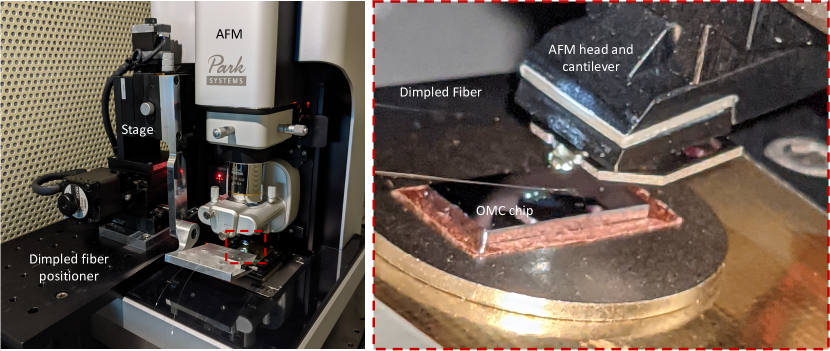
To enable in-situ nano-oxidation and real-time tuning of OMC cavities, an optical test setup has been integrated into the enclosure of an AFM as shown in Fig. 5. The system has three sub-parts that are controlled independently: 1) the optical fiber positioning system, comprising a three-axes linear motorized positioning stage and two rotational positioning stages, 2) the sample mount of the AFM with x and y motional degrees of freedom, and 3) the AFM cantilever with z motional degree of freedom. Additionally, the AFM enclosure is equipped with a temperature and humidity sensor to ensure that environmental conditions are within the desired regime. The entire assembly sits on an optical table to minimize vibrations during the oxidation process.
5.2 Characterization of nano-oxidation
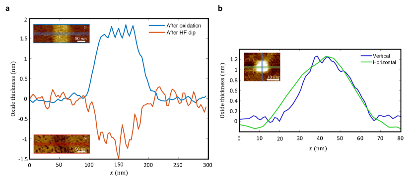
The nano-oxidation process generates oxide beneath and above the surface of silicon. Here we describe the procedure used to assess the ratio of oxide height and depth above and below the silicon surface, respectively. We first measure the post-oxidation height by performing AFM scans in the tapping mode. Subsequently, we etch the oxide in an anhydrous hydrofluoric acid vapor etching tool (SPTS PRImaxx uEtch), and perform AFM scans of the resulting trenches in silicon. The data obtained, as depicted in Figure 6a, indicates that the oxide thickness beneath the surface is approximately 70 of the total measured thickness above the surface. Figure 6b shows the characterization of a single oxide pixel generated in the mild oxidation mode. The size of the pixel is approximately 25nm along both x and y axes. We utilize such oxide pixels for fine-tuning of both optical and acoustic resonances in real-time as discussed in the main text.
5.3 Effect of nano-oxidation on optical Q factor
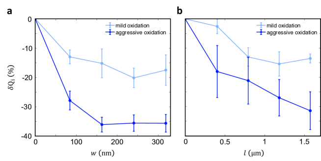
In addition to altering the mechanical and optical characteristics of the local silicon surface, the nano-oxidation process can introduce roughness and additional scattering sites. Consequently, we observe a reduction in the optical Q-factor during our coarse tuning experiments. As shown in Figure 7, the reduction in Q-factor is more pronounced upon increasing the size of the oxidation patterns and the thickness of the oxide layer. For optics-focused patterns generated in regions with high electric field intensity, we observe a substantial impact on the optical Q-factor. A maximum reduction in of approximately 35% is noted for the aggressive oxidation case when 300 nm. For the mild oxidation case, the reduction in is less than 20%. In the case of the acoustics-focused pattern, the reduction in is less than 35% for aggressive oxidation case, and less than 20% for mild oxidation case when 1.5 m.
5.4 FEM simulations for pixel-by-pixel oxidation and selectivity analysis
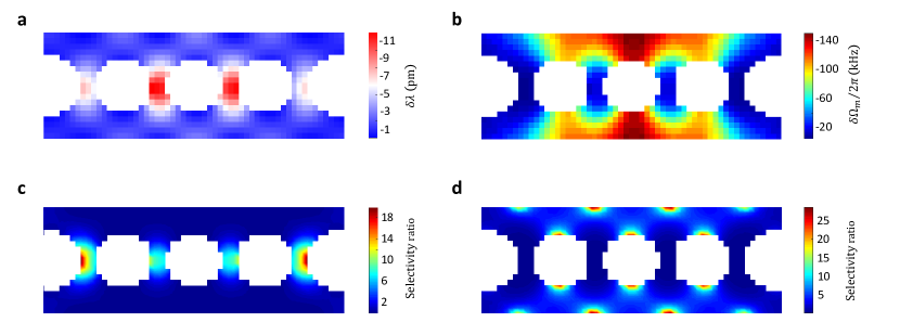
Figure 8a and b show the results of FEM simulations where we mapped out how the location of a single oxidation pixel affects the optical wavelength and acoustic frequency, respectively. These profiles closely match the optical intensity and acoustic displacement profiles shown in Fig. 1. This is expected because oxidation at points with larger optical field concentration leads to larger change in optical energy, and thereby in the optical resonance wavelength. Similarly, oxidation at the points of maximum displacement leads to a larger fractional change in effective mass of the acoustic mode, and thereby in the acoustic resonance frequency. The exact material properties of the thin film oxide such as the density, Young’s modulus and relative permittivity are specific to the oxidation process. In our approach, we use these material properties as variables and then we find what scaling allows us to match the coarse tuning experiment (Fig. 2) and simulations. This way, we found that the density, Young’s modulus and relative permittivity of oxide are 3500 kg/, 70 GPa and 2, respectively. In the acoustic simulations, we use the anisotropic elasticity tensor of silicon with () = (166, 64, 80) GPa and assume a [110] crystallographic orientation for the x-axis.
In Figure 8c and d, we plot the normalized optical selectivity, and normalized acoustic selectivity, . Here, and are normalized with respect to the maximum value calculated in the pixel-by-pixel oxidation profiles in Figure 8a, b. In the case of fine tuning experiments where we seek small frequency shifts, we concentrate on the high selectivity regions. However, the locations with maximum optical selectivity, do not coincide with those that produce maximum optical tuning . Likewise, the regions with maximum acoustic selectivity are relatively small and localized at the edge of the silicon-air boundary. As a result, for coarse tuning experiments, it is more practical to use large oxide patches as opposed to individual pixels to achieve large tuning at the expense of selectivity. Details of the pattern generation algorithm used to generate the large oxide patches are given in Appendix E.
5.5 Nano-oxidation inverse pattern generation algorithm.
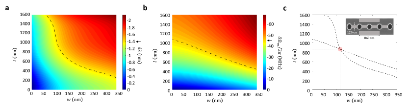
The results from coarse tuning experiments in Fig. 2 of the main text show frequency shifts generated by either the optics-focused or the acoustic-focused pattern type. In practice, we require a union of both types of patterns to tune both optical and acoustic resonances. To enable the generation of such joint patterns, we first interpolate results from coarse oxidation experiments to create an oxidation map with frequency shifts measured with just the optics-focused and acoustic-focused patterns. Our inverse pattern generation algorithm uses this map to find a suitable joint pattern to target the desired simultaneous shift in optical and acoustic resonances. The pattern search begins with mild oxidation patterns and progresses to aggressive oxidation patterns if larger frequency shifts are desired. A pattern is deemed suitable if the calculated resonance shifts can target the desired optical wavelength to within 200 pm and the desired acoustic resonance to within 5 MHz. The pattern generation maps presented in Fig. 9a,b correspond to the aggressive optical - aggressive acoustic oxidation scenario. There are three other pairs of pattern generation maps corresponding using mild optical - mild acoustic, mild optical - aggressive acoustic, and mild optical - aggressive acoustic oxidation scenarios. To illustrate the pattern search process, Figs. 9a, b show contours corresponding to an example scenario where shifts, nm and MHz, are desired. As shown in Fig. 9c, the intersection of these two contours allows us to estimate the required joint pattern with a width, 120nm for the optics-focused component and length, 860nm for the acoustics-focused component.
5.6 Simultaneous tuning of three OMCs: step-by-step process
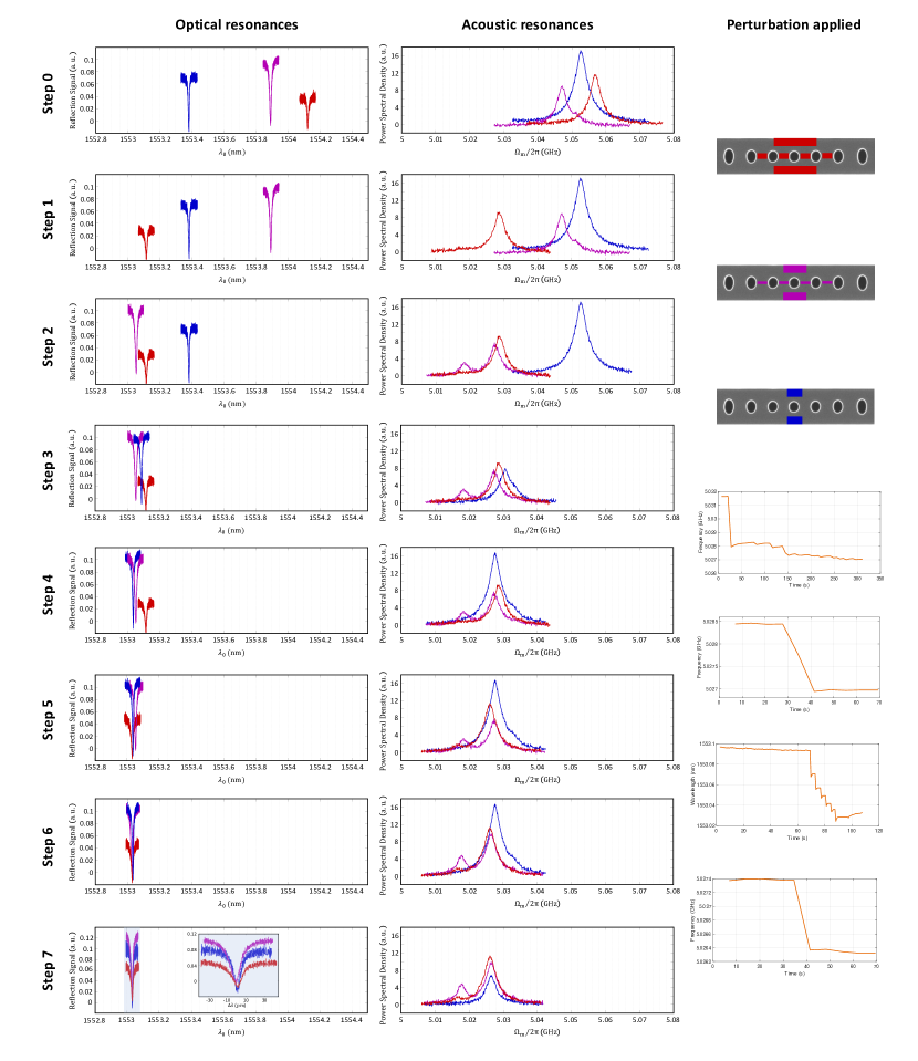
In this section, we describe in detail the step-by-step tuning protocol used for frequency alignment of three OMC cavities. This involves a series of coarse tuning steps followed by real-time fine tuning steps. The experimental results for each step are shown in Fig. 10.
-
1.
Step 0: We started with three OMC cavities (red, magenta, blue) whose optical wavelengths and acoustic frequencies are = (1553.891, 1553.381, 1553.123) pm and = (5.057, 5.047, 5.053) MHz respectively.
-
2.
Step 1-3: We feed and to the inverse pattern generation algorithm which generates patterns to tune each OMC to the target frequencies.
-
3.
Step 4-7: At the end of step 3, all 3 OMC cavities are within a suitable range for fine tuning (typically 200 pm and 5 MHz for optics and acoustic resonances). We then employ pixel-by-pixel oxidation to fine tune the resonances while monitoring their values in real-time. The corresponding real-time wavelengths and frequencies are shown in the right most column of Fig. 10.
At the end of three coarse and four fine tuning steps, we achieve optical wavelengths of 1553.031 nm, 1553.029 nm and 1553.031 nm and acoustic frequencies of 5.0261 GHz, 5.0264 GHz and 5.0266 GHz for the three OMCs. This indicates simultaneous optical wavelength and acoustic frequency matching within 2 pm and 500 kHz, respectively.
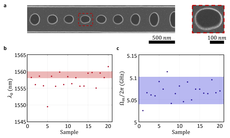
5.7 Frequency distribution of fabricated devices
The OMC cavity design in this study incorporates geometric features with critical dimensions smaller than 100 nm. In our fabrication process, electron beam lithography and reactive ion etching offer a feature size precision of approximately 5 nm [1]. In Figure 11a, a scanning electron microscope (SEM) image of a randomly selected OMC highlights geometric imperfections in the fabricated device. To assess how these imperfections manifest in the measured optical and acoustic resonances, we fabricated 20 devices with nominally identical geometry positioned adjacent to each other on a chip.
Figures 11b and c show the measured optical wavelengths with a standard deviation of 2.58 nm and acoustic resonance frequencies with a standard deviation of 19.8 MHz, respectively. The highlighted area in Figures 11b (c), with a tuning range of 2 nm (60 MHz), signifies the number of devices that can be brought into resonance solely through optical (acoustic) tuning. The data indicates that approximately 50% (90%) of OMCs fabricated with the identical geometric design can be frequency-matched optically (acoustically) after fabrication.