Measurements of time resolution of the RD50-MPW2 DMAPS prototype using TCT and
Abstract
Results in this paper present an in-depth study of time resolution for active pixels of the RD50-MPW2 prototype CMOS particle detector. Measurement techniques employed include Backside- and Edge-TCT configurations, in addition to electrons from a source. A sample irradiated to \fluencewas used to study the effect of radiation damage. Timing performance was evaluated for the entire pixel matrix and with positional sensitivity within individual pixels as a function of the deposited charge. Time resolution obtained with TCT is seen to be uniform throughout the pixel’s central region with approx. at of deposited charge, degrading at the edges and lower values of deposited charge. measurements show a slightly worse time resolution as a result of delayed events coming from the peripheral areas of the pixel.
1 Introduction
In recent years the research and development of silicon detectors for tracking purposes in high energy physics experiments has shifted to include not only requirements for high spatial resolution and sufficient radiation hardness, but also accurate time resolution [1]. With the forthcoming upgrades of the LHC to higher luminosities (HL-LHC [2]) and plans for the FCC [3], accurate temporal information will play an important role in tracking, as spatial information alone is insufficient for adequate performance at the expected increased spatial density of collisions. For example, during the Phase-II upgrade of the ATLAS experiment [4], a new High Granularity Timing Detector will be installed to provide track time information with a resolution below [5], enhancing the performance of the planned new tracking system. Various studies of time resolution dealing with different silicon detector technologies have already been carried out, see for example [6], [7] and [8].
In this paper, measurements of time resolution of a Depleted Monolithic Active Pixel Sensor (DMAPS) prototype are presented. As a promising alternative to the well-established hybrid silicon detector, DMAPS technology features a single-wafer design with readout electronics integrated directly onto the sensing chip [9]. This configuration provides potential benefits including lower cost, shorter time of production and a lower material budget within the tracking volume, all important aspects for future trackers with large sensor area requirements. DMAPS technology is therefore being considered for use in future high-rate and high-radiation environments that such trackers would face.
Within the studies of the prototype, time resolution of a monolithic sensor was measured for the first time using focused pulsed laser light in Back- and Edge-TCT [10] configurations, allowing for position-sensitive measurements of the time resolution within the depleted region. Measurements were also performed with a setup using electrons from a radioactive source. In all cases the time resolution was determined as a function of the amount of charge collected on the input of the readout electronics.
2 RD50-MPW2 prototype
Characterization of time resolution was performed with a prototype detector named RD50-MPW2 produced by the CERN-RD50 collaboration [11] that is shown in figure 1. It is the second prototype in the series of HV-CMOS monolithic detectors that the collaboration is developing with the goal of studying and improving the technology for future tracking applications in particle physics experiments [12]. The prototype is manufactured in a HV-CMOS process from LFoundry on thick p-type substrate silicon wafers with varying initial resistivities; samples with an initial resistivity of were selected for measurements in this work. In order to study potential effects of radiation damage on the time resolution, a sample irradiated with reactor neutrons was measured alongside unirradiated ones. Irradiations were conducted with neutrons to a neutron equivalent fluence of \fluencewith the TRIGA nuclear reactor at Jožef Stefan Institute (JSI) in Ljubljana [13, 14]. During neutron irradiation, samples were also exposed to a total ionizing dose of about .
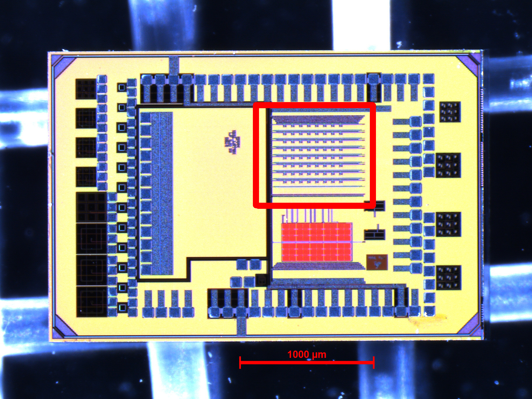
Measurements were made with the matrix of active pixels, marked with a red square in figure 1. Each pixel in the matrix has a size of and contains an analog readout circuit. The circuit consists of a Charge Sensitive Amplifier (CSA) and a comparator with a 4-bit trim-DAC for correcting threshold variations arising from manufacturing nonuniformities. Two types of pixels are implemented in the matrix, differing by the way the CSA is reset. For most measurements in this study, the so-called continuous reset pixel (columns in the matrix), shown in figure 2, was chosen due to its output signal Time Over Threshold () being linearly proportional to the collected charge. This is achieved by the constant current source linearly discharging the feedback capacitor storing the collected charge. In the other type of pixel, called the switched reset pixel (columns ), the feedback capacitor is discharged via a much larger current controlled by the comparator output. Additionally, all pixels chosen for time resolution measurements were required to have neighboring pixels on all sides to avoid any edge effects.
Configuration and biasing of the chip is implemented via the CaRIBOu system [16, 17], which enables setting various voltages and DAC values of the pixel matrix. For the studies presented here, a comparator baseline of was used at two threshold voltages of , corresponding to a threshold in electrons of respectively for trim-DACs set to [18]. Considering a breakdown voltage of passive structures at around [19], the bias voltage was set to for all measurements.
Time walk properties of the prototype were already characterized in [18], with measurements showing a good in-time efficiency (delays below ) across the entire range of collected charge and no significant loss of performance after neutron irradiation. In terms of characterizing the RD50-MPW2 performance, this paper augments the aforementioned results and presents an in-depth study of the time resolution.
2.1 Output signal calibration
Each pixel within the matrix contains a calibration circuit enabling the injection of charge into the front-end electronics. Charge is injected by connecting a voltage step function via an injection capacitance with a value of . The amount of injected charge can then be determined as , where is the amplitude of the voltage step function.
By varying , a calibration of the comparator to the amount of injected charge can be performed. For example, figure 3 shows calibration curves for pixels later selected for time resolution measurements with the Edge-TCT method. The data points show a large variation of values between the two pixels. However, by measuring multiple pixels across the matrix and comparing their outputs before and after irradiation, it was shown that irradiation does not affect the outputs significantly [18]. The differences seen in figure 3 are therefore mostly a result of deviations in the CSA gain (feedback capacitance) arising during the production of samples. Consequently, individual calibration of each pixel measured is necessary for correct determination of collected charge.
3 Time resolution measurements
Measurements of time resolution were performed with the Transient Current Technique (TCT) using a pulsed and focused laser beam with a of less than at the focusing point. By focusing the incident laser light, free charge carriers can be created at different positions within the depleted region of the pixel, thus enabling determination of time resolution as a function of the position where the charge was created. To perform these position-sensitive measurements, the carrier board is placed onto precision stages with a movement accuracy below . The time resolution was measured using two different setups varying by the incident laser beam orientation.
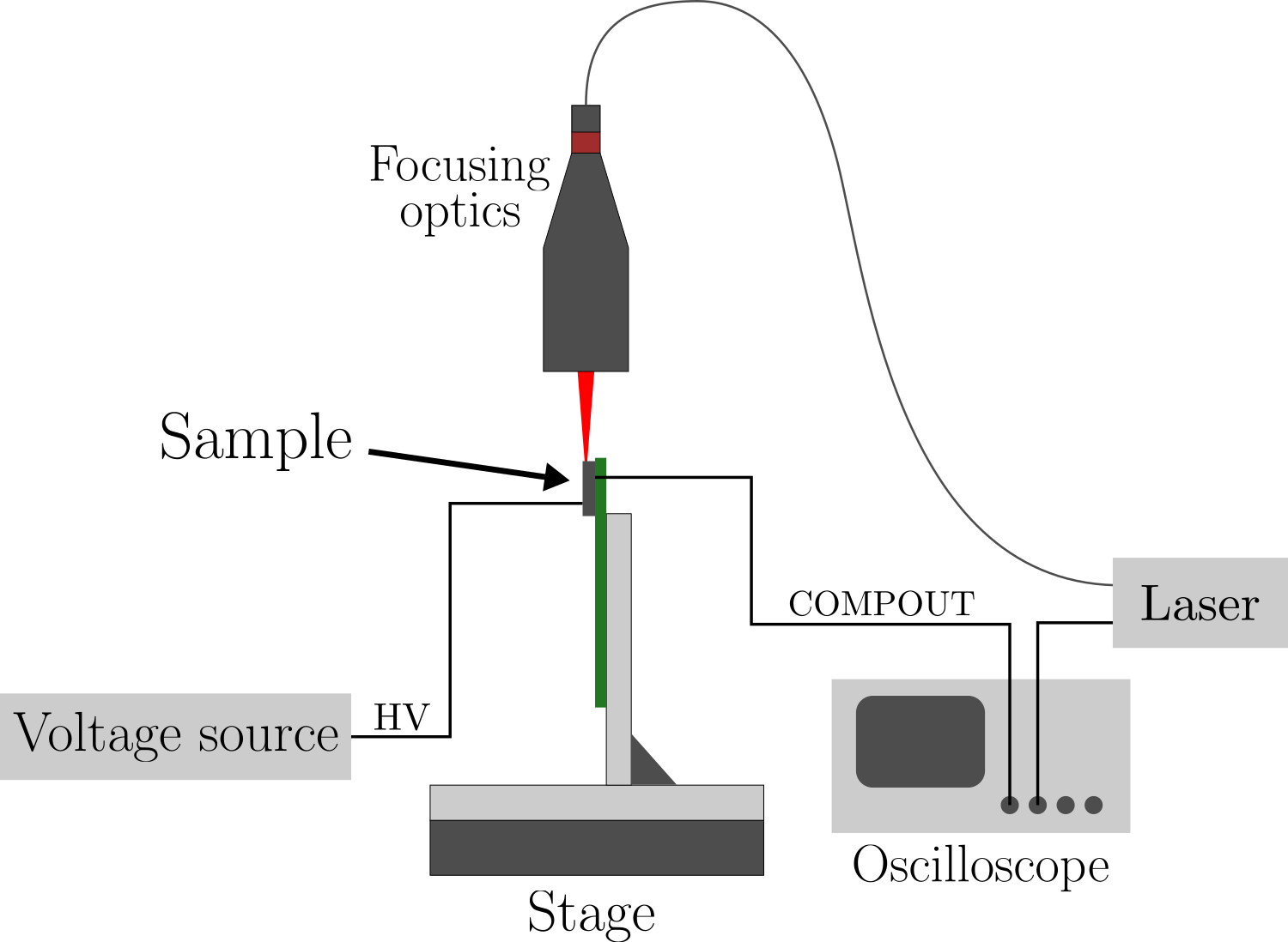
Backside-TCT measurements were performed with a laser setup located at Nikhef. A schematic of the setup is shown on the left in figure 4. The light is injected into the sensor backside through a hole in the carrier PCB. The laser is driven via a pulse generator that was kept on a rise and fall time of , a pulse width of , and an amplitude of . The laser intensity was adjusted via a variable optical attenuator controlled via a power supply. Both the comparator output and the pulse generator signal are recorded using a DSO3000 series oscilloscope with a bandwidth and a sampling rate.
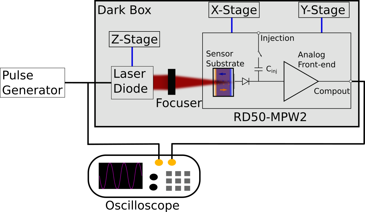
Edge-TCT measurements were performed at the JSI laboratories using a modified version of the Particulars setup [20] shown on the right in figure 4 (more details on the setup can be found in [18]). In this setup, laser light with a pulse duration of was oriented to enter the sample from the side edge of the sample. Signals were sampled with a DRS4 oscilloscope with an analog bandwidth of and sampling rate of .
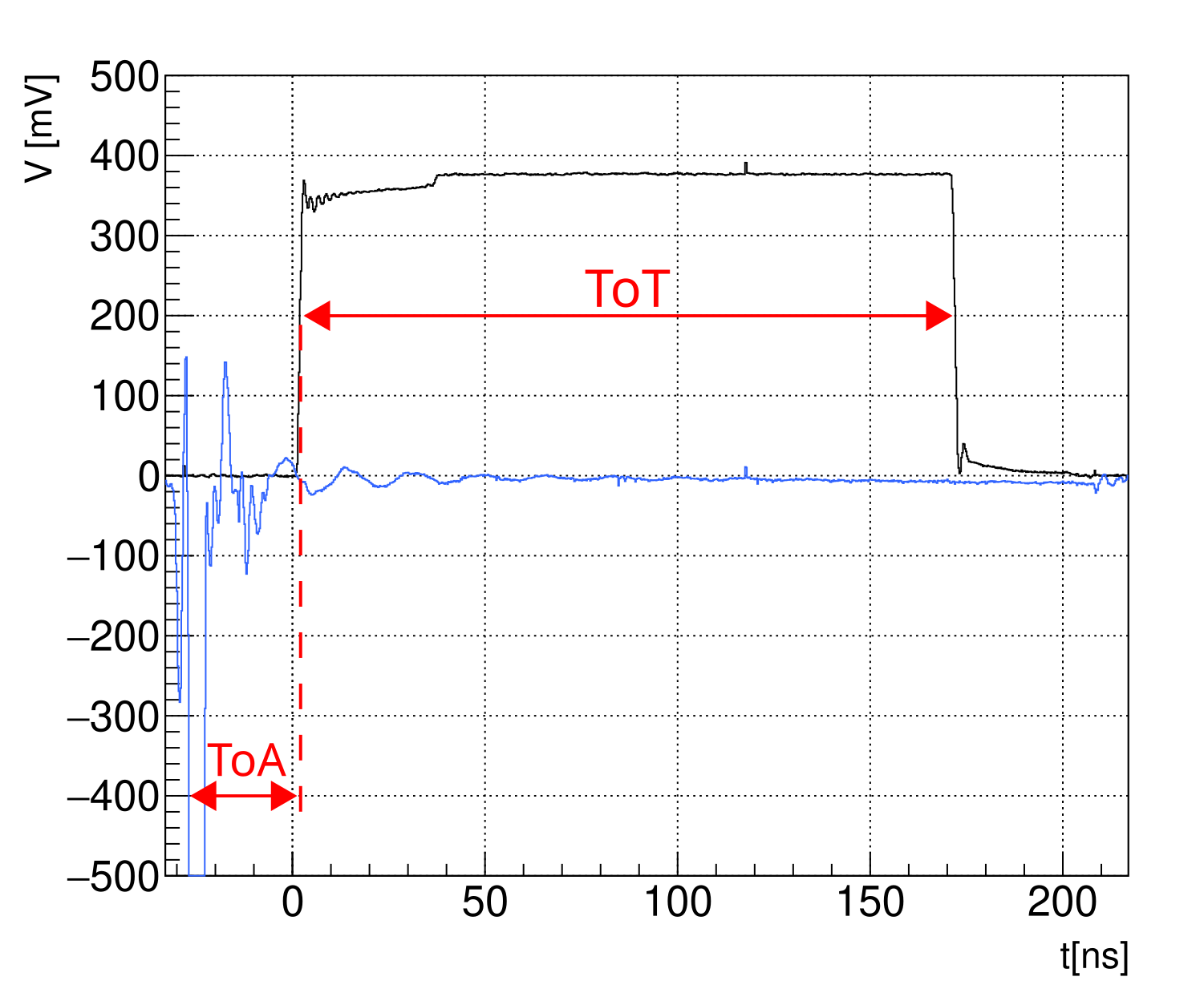
A signal from the pulse generator (laser driver), which generates the laser pulses, was used as a time reference for determining the arrival time of the pixel response. Figure 5 shows a typical event. The time of arrival () of the pixel response relative to the reference signal is determined as the difference of level crossing times over a fixed threshold. The of the pixel output is also recorded and used for determining the amount of collected charge using the calibration curves described in section 2.1. The time resolution is obtained as the standard deviation of the arrival times () over multiple collected events. is only determined up to an additive constant, which is affected by optical fiber and cable lengths. This, however, does not affect the time resolution calculation, since only the relative spread of these times is of interest.
The total time resolution of a detector is a result of various contributions [1] and can be written as their sum
| (3.1) |
where is the effect of Landau fluctuations and the effect of signal distortion due to non-uniformities in the weighting field and charge carrier drift velocities. The contribution from time walk is not relevant in this case since the time resolution was measured as a function of collected charge (i.e. at constant signal pulse amplitudes). The jitter of the electronics is given by the expression [21], where is the signal rise time and the signal-to-noise ratio, giving a dependence on the collected charge.
3.1 Time resolution with Backside-TCT
For measurements of time resolution with Backside-TCT, two types of measurements were performed on an unirradiated sample using the laser setup: a scan over the entire pixel matrix and an in-pixel position-sensitive scan. For all measurements the laser was focused on the pixel center444The center of a pixel is determined via a simple scan in and by taking the midpoint between the edges corresponding to a drop in the pixel response. and moved along the row and column direction to perform the full matrix and in-pixel scan. Each measurement step includes at least 50 measured waveforms triggered on the pulse generator and measurement steps with fewer than 10 total responses of the comparator output registered in the waveforms are discarded.
3.1.1 Full matrix
All measurements of the full matrix are conducted with trim-DAC optimized settings and the comparator threshold set to . Taking the trim-DAC adjustments into account, the effective thresholds of the two pixel flavors at trim-optimized settings differ from one another, with switched reset pixels showing an effective threshold of while continuous reset pixels show a threshold of [22].
The left side of figure 6 shows the time resolution achieved for the full pixel matrix split into their row and column ID at a laser induced charge injection value of about . Overall the response of the pixel matrix is uniform, showing a time resolution of about for all pixels with the exception of row 0 and column 7 which show a worse time resolution. A look at the measured of each pixel, depicted in the right plot of figure 6, shows that the measured in row 0 and column 7 are far lower relative to the response measured by the other pixels. This discrepancy was also present upon repeat of the measurement. A further investigation with an in-pixel measurement showed that both the amount and location of maximum induced charge value for pixel 555Pixel locations are given as values. is further than away along the column from the center of pixel . This is most likely due to the electric field of the pixels at the edge of the matrix not being constrained by surrounding structures resulting in a non-uniform response of the pixel. The response differs for the four edges, as the structures surrounding the matrix also differ from one another on all sides. This was confirmed with an in-pixel measurement of which gathered charge from larger distances than expected while having a lower charge response in the pixel center than pixels located in the central matrix. As a result, in all further measurements only the central matrix is shown to avoid these boundary effects.
Another effect visible in figure 6 is a far lower for the right half of the matrix. This is due to the different pixel flavor as the switched reset pixels are drained far quicker once the signal reaches the threshold [12]. As such the linearity between charge and is not fulfilled. This has no impact on the time resolution but all values of charge refer to the results given by the continuous reset pixels after to charge conversion from the calibration for which the linearity is true.
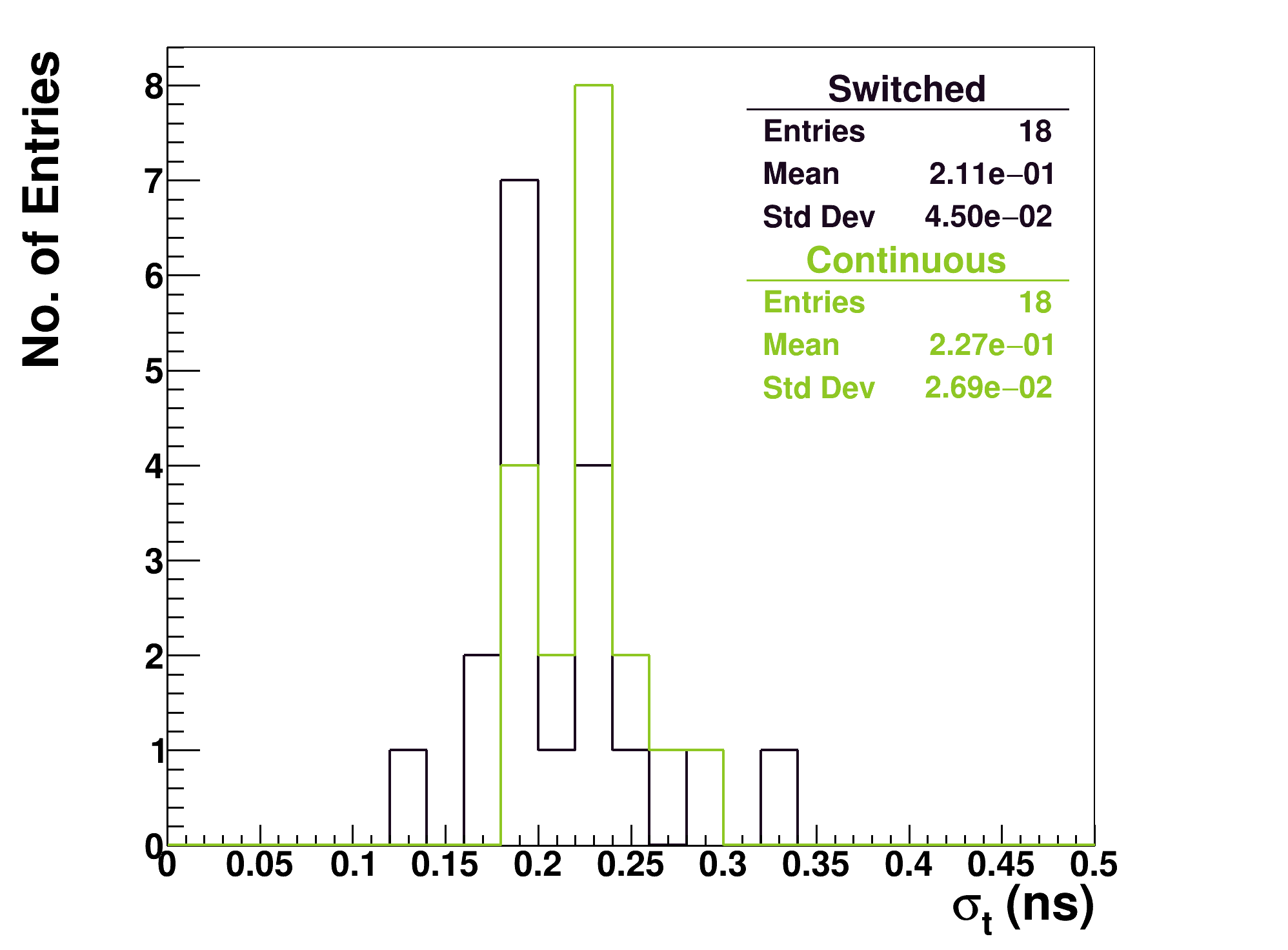
The core of the matrix shows good agreement between the time resolution of the switched reset pixels and the continuous reset pixels, see figure 7. The switched reset pixels show a mean time resolution of compared to the continuous reset pixels which have a time resolution of . Though there is a small difference, the two pixel flavors time resolutions are still within the error of one another. The measurements are also congruent with the results achieved through direct charge injection only probing the front-end which is on the order of and ; the slightly worse performance of the continuous reset pixels results from different thresholds for the two types of pixels.
3.1.2 In-pixel
Multiple in-pixel measurements were performed for different pixel flavors. Shown here are the results for the continuous reset pixel which is located in the inner matrix core on the boundary changing the pixel flavor to the switched reset pixels.
The charge injected via laser was slightly above the value injected via the full matrix scan. The time resolution achieved via the in-pixel scan is depicted in figure 8. The red square corresponds to the pixel boundary while the yellow square corresponds to the collection well. The area within the pixel boundary shows a flat time resolution of about beneath the collection well and a time resolution of within the pixel boundary. The slightly improved resolution is due to the aforementioned slightly higher charge injection value of . The results show some charge sharing up to a distance of with the given statistics.
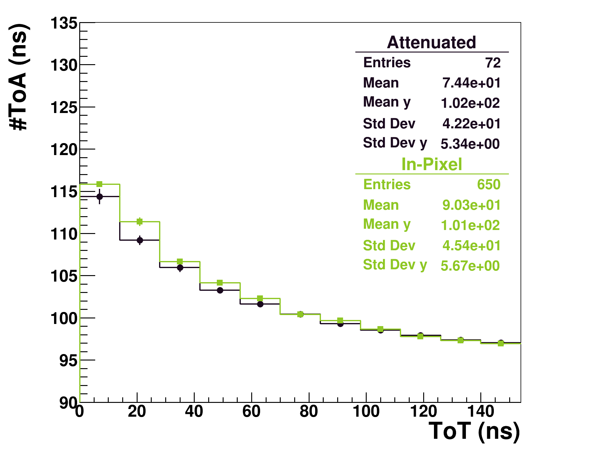
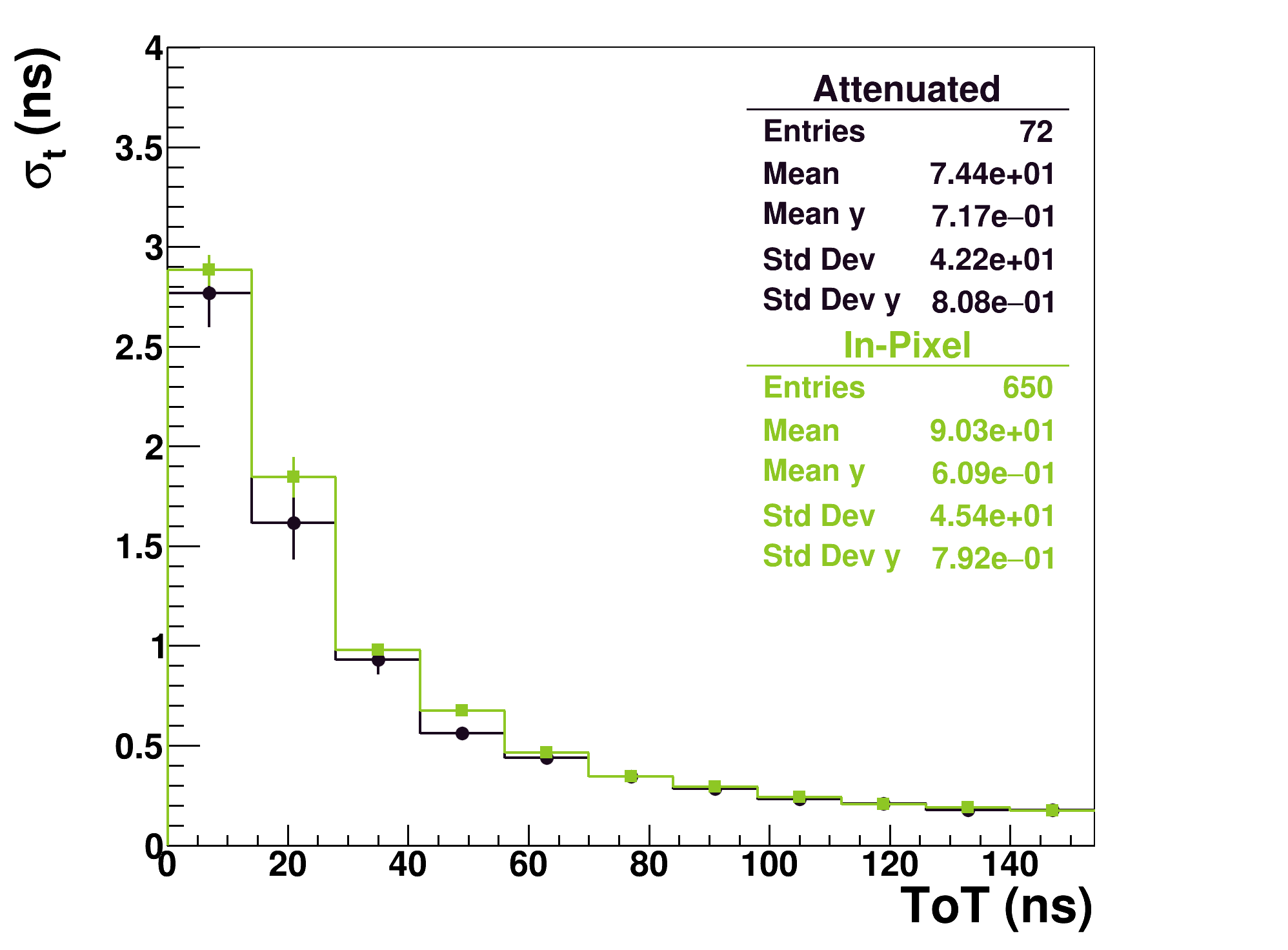
Beyond the pixel boundary, the time resolution begins to drop rapidly. However, further investigation is needed to determine whether the increased and at the edge are purely due to increased time walk as a result of lower charge, or whether the geometric distance to the collection well adds an additional contribution. For this purpose, the measured and gathered via the in-pixel measurements are compared with a measurement in which the laser was kept focused on the pixel center and the injected charge was adjusted via the optical attenuator. These comparisons are depicted in figure 9 for the (left) and the (right). Both distributions show excellent overlap at high values at which point the in-pixel scan is also located over the center of the pixel. However, at values below the measured and from in-pixel measurements begin to rise faster than the results gathered via the centered attenuated signal. At low , measurements are performed close to the threshold which also increases the statistical uncertainty of the measurements. Nonetheless, at very low charge values, the expected differs by up to on average while the time resolution is worse by indicating a contribution from fluctuations due to inhomogeneous charge collection times. While not too relevant for laser measurements focused on the pixel center, measurements with beam particles or radioactive sources will be affected by this additional contribution.
3.2 Time resolution with Edge-TCT
In the Edge-TCT setup, measurements were performed on single pixels without trim-DAC optimization (all trim-DACs were set to 0). Two-dimensional profiles of time resolution for the unirradiated and irradiated samples are presented in figure 10 for different laser beam intensities. The width of the measured profiles is consistent with the size of the pixels with some charge sharing beyond the pixel boundary present, as was seen in the Backside-TCT measurement. The depletion depth decreases with irradiation due to the increase of the effective space charge concentration [19]. At the highest laser intensities, the time resolution reaches a value of around , while at low intensities, it degrades to a value above . Time resolution values are similar throughout the center of the depleted region, indicating consistent charge collection independent of the initial location of deposition, while in the charge sharing region on pixel edges, time resolution degrades as was also seen in results from Backside-TCT. The relatively broad smearing of the edges is mainly due to a finite laser beam width and suboptimal focusing on account of the pixel matrix being positioned deep within the chip, possibly causing beam reflections before the light reaches the pixel. This is also the likely cause of an irregularity in the unirradiated sample seen at .
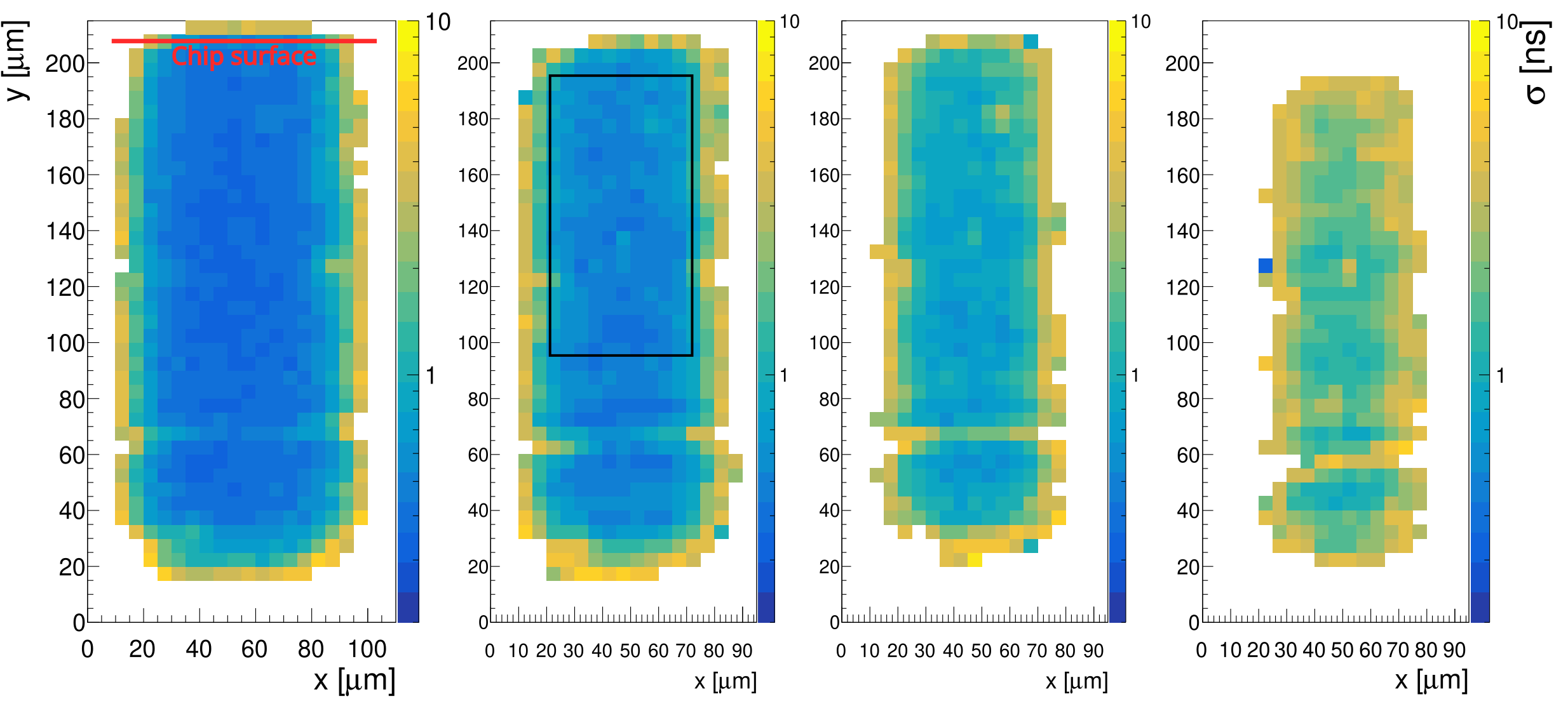
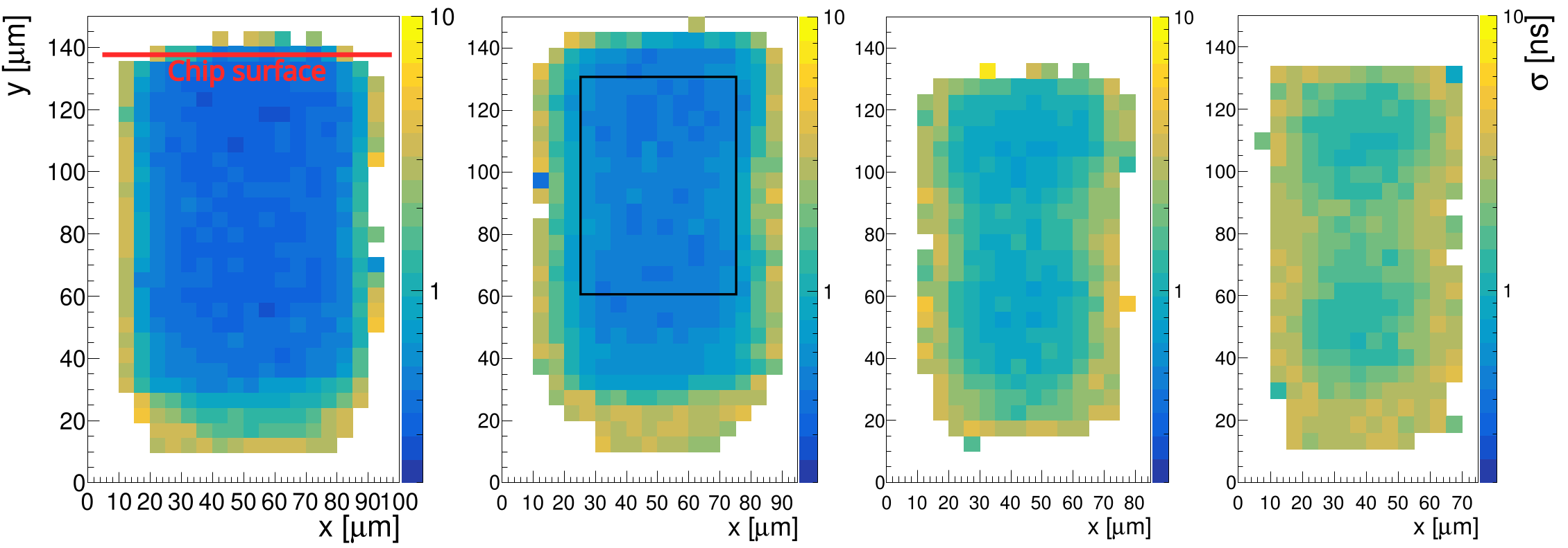
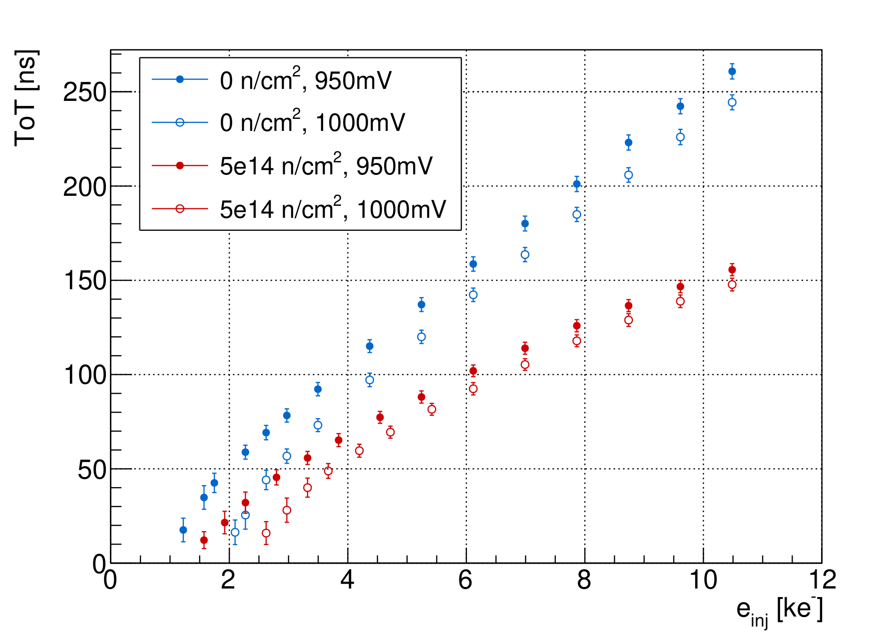
To better assess the time resolution, points from the central, most efficient volume wide and () in depth for the unirradiated (irradiated) samples starting below the chip surface (regions marked with a black rectangle in figure 10) are selected and plotted as a function of the collected charge obtained from the average value at each point. Two-dimensional scans were taken at both threshold levels and several laser beam intensities were used to cover the entire range of collected charge values. Results in figure 11 show a time resolution better than for charges above in all cases and reaching approximately at the highest measured charge of . At low charge, the time resolution degrades with the point of divergence depending on the comparator threshold setting. Points of divergence give thresholds in electrons and are consistent with results obtained by activation curve scans in [18], which were done by injecting a variable amount of charge via the calibration circuit and determining the minimum charge at which the pixel starts producing an output signal. At the measured depletion depths, the charge deposited by a MIP has a most probable value of () for an unirradiated (irradiated) sample, which is large enough to lie within the asymptotic part of the pixel’s time resolution dependence and thus provide a good expected timing performance for MIPs. Irradiation to \fluencedoes not indicate any significant degradation of performance; the increase of the point of divergence comes from the lower CSA gain as discussed in section 2.1.
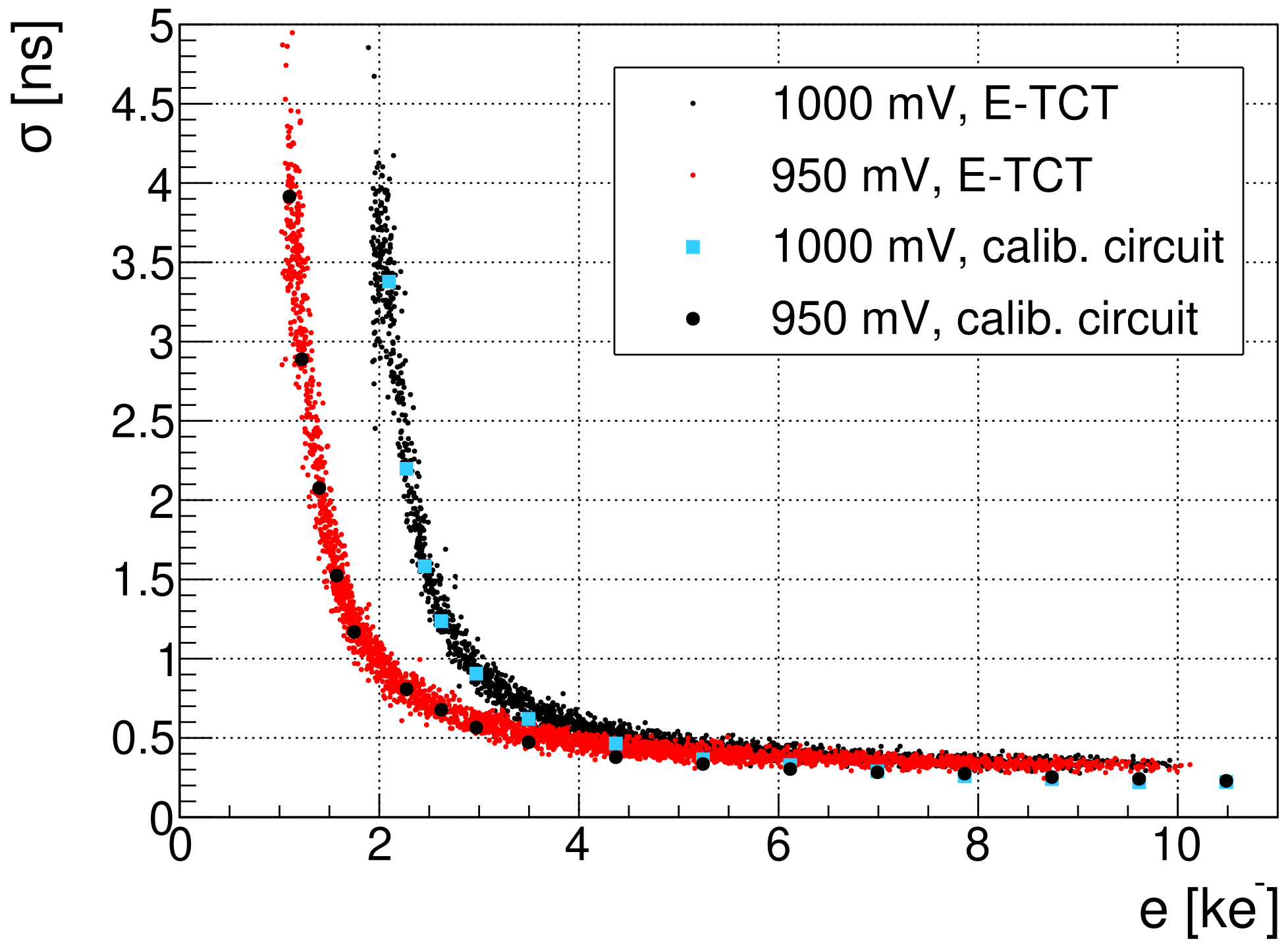
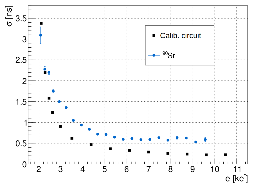
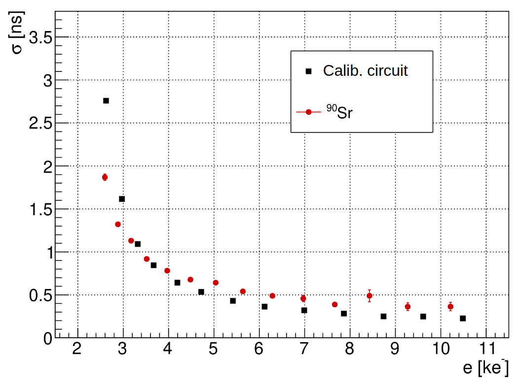
The time resolution was also determined by using the pixel’s calibration circuit. Since the charge is injected directly in front of the readout electronics, the charge collection in the sensor is not present in this case, making the jitter of the electronics the main contribution to the time resolution. Comparing these measurements with the Edge-TCT results, a general good agreement of values is seen between the two methods, indicating that the time resolution is dominated by the electronics jitter. A slight increase in the resolution seen at charges above can be attributed to other effects from the charge collection phase, or possibly variations in the intensity of successive laser pulses.
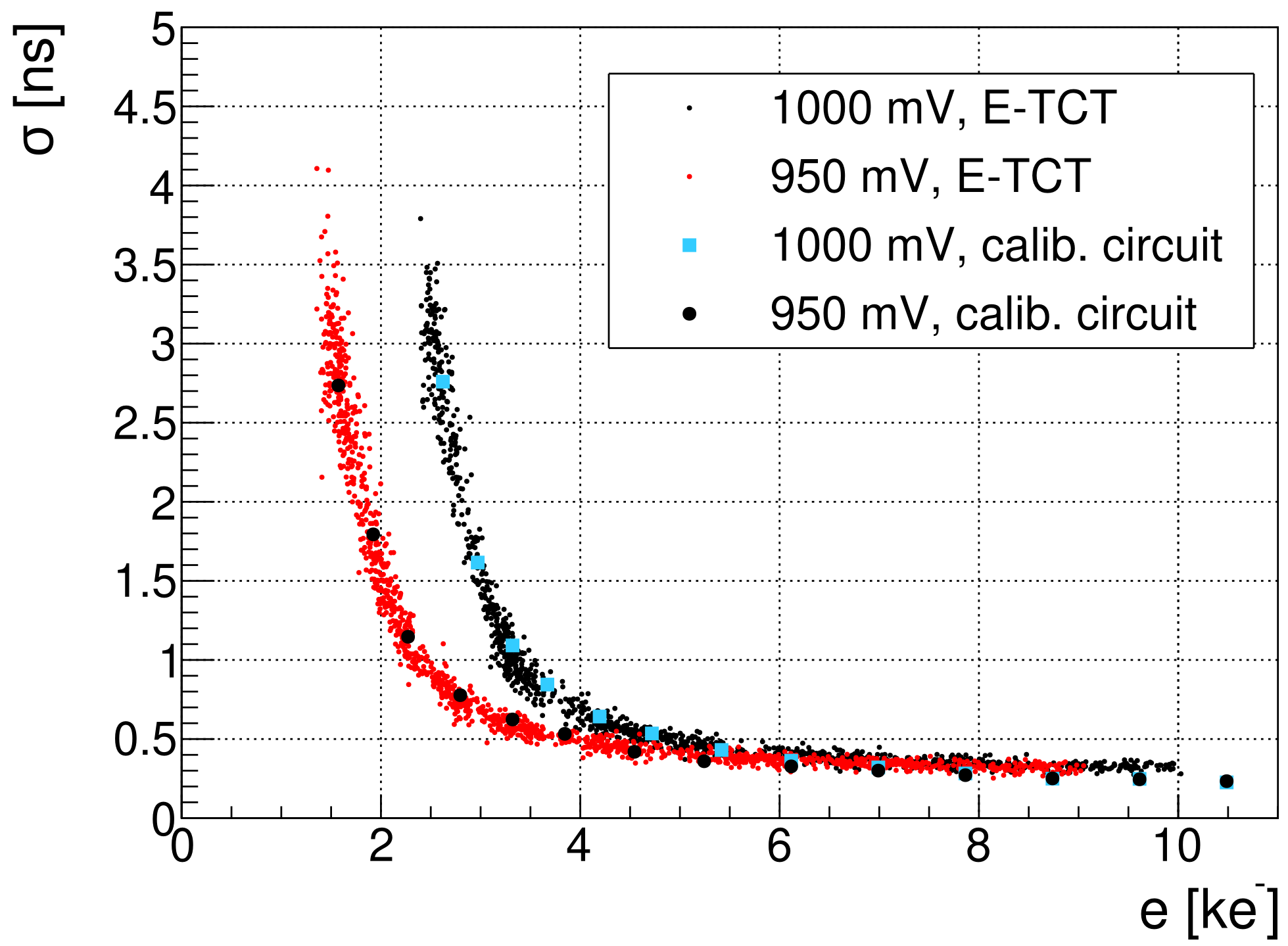
A comparison between Edge-TCT measurements performed at JSI with Backside-TCT measurements from Nikhef for a single pixel are depicted in figure 12. While both measurements use a comparator threshold of , the trim-DACs at JSI are kept at 0, resulting in a threshold of . At Nikhef, the trim-DACs are increased in order to equalize the thresholds between pixels due to the investigation of the full matrix, resulting in a higher average threshold of for the continuous reset pixels. Overall, the behavior of the two measurements is in good agreement showing similar behavior when the laser induced charge is close to the respective pixel thresholds.
3.3 Time resolution with
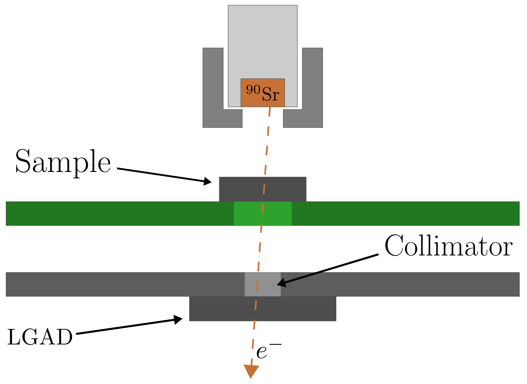
Time resolution was also determined by using electrons from a source. A schematic of the setup used in this case is shown in figure 13, which follows a similar layout that was used in [23] and [24]. The reference signal is provided by a second silicon detector mounted behind the sample. For a minimal impact on the overall time resolution of the system, a thin Low Gain Avalanche Detector (LGAD) with a pad size of and a time resolution of around , mounted on a timing board developed by University of California Santa Cruz [25], was used for this purpose. A collimator is positioned in front of the reference LGAD to only select electrons that pass through the device under test and create a sufficient amount of charge in the reference detector, filtering out electrons from the lower end of the energy spectrum that do not behave as MIPs.
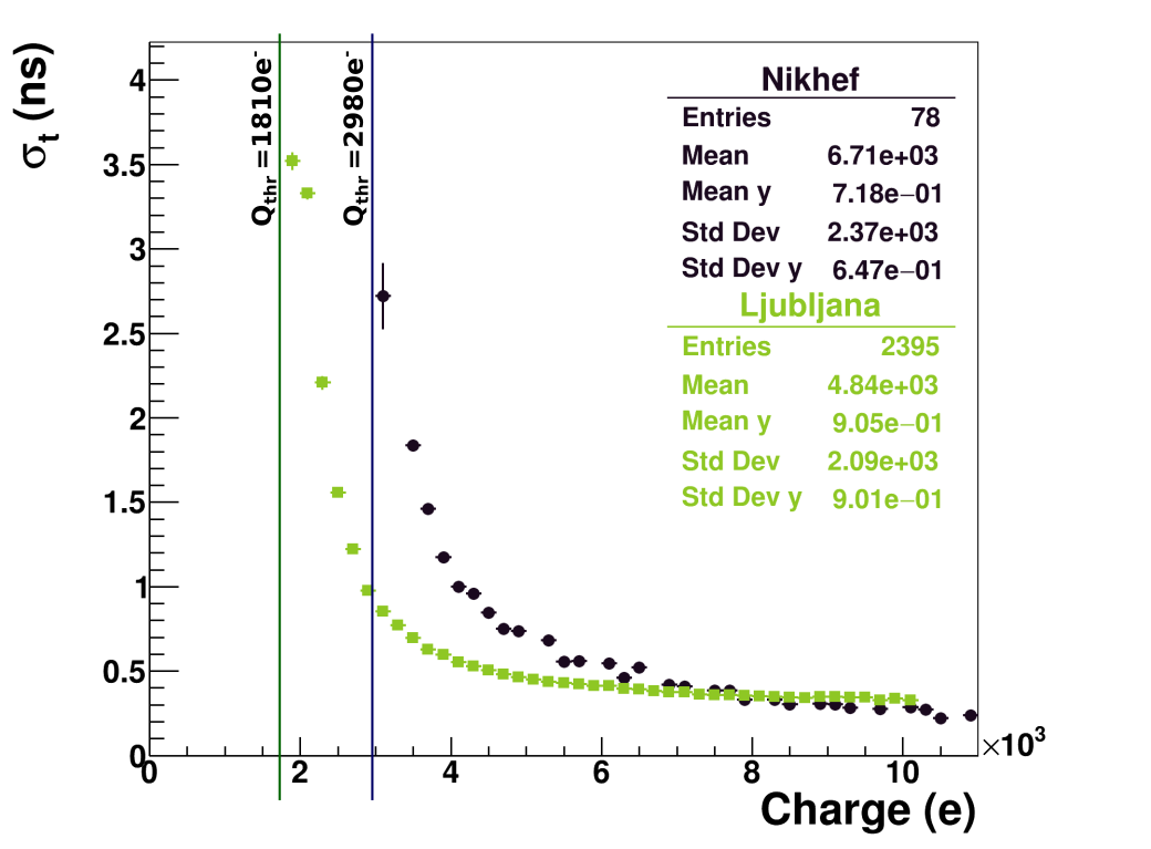
The acquisition was triggered on coincident signals in both channels. Due to the small pixel size in the RD50-MPW2, the hit rate was limited to using an source. To eliminate any time walk effects on the reference detector, constant fraction discrimination at of the maximum was used in the offline LGAD signal analysis. The time resolution is again obtained as the standard deviation of the distribution. In this case, an extra contribution to the measured time resolution arises from the reference detector . Due to the markedly better time resolution of the LGAD, the second term can be neglected.
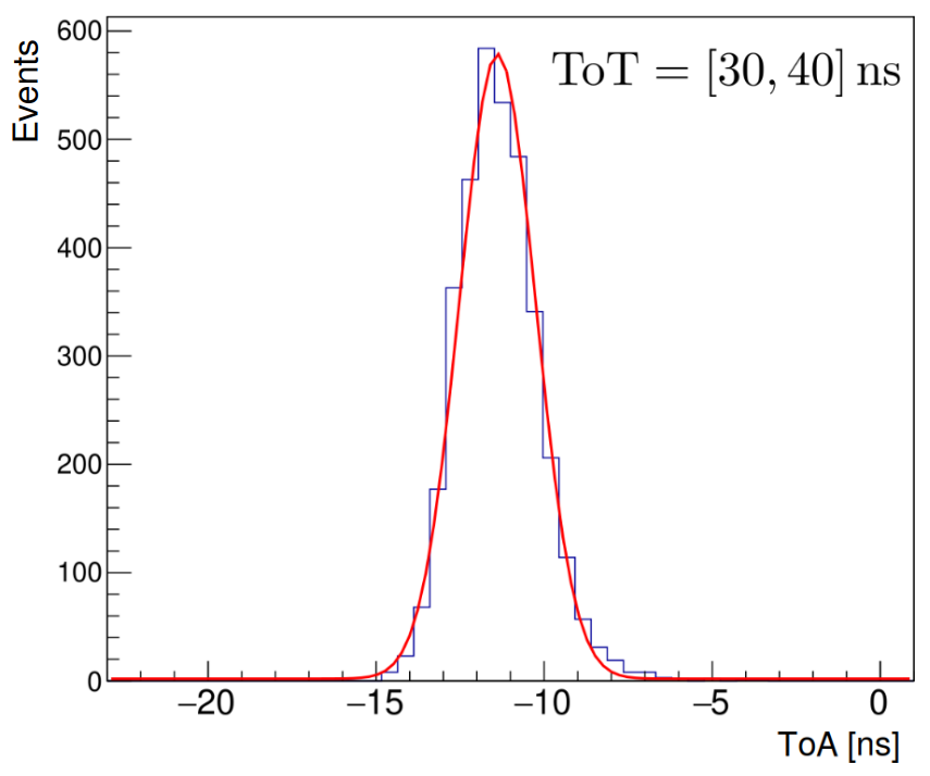
Since electrons from the source deposit a variable amount of charge within the pixel, the dependence of the time resolution on the collected charge is determined by sorting all measured coincidence events by their value of the comparator output and binning them into wide bins. Within each bin, the distribution of arrival times is fitted with a Gaussian curve with its standard deviation representing the time resolution (see figure 14). Results at a threshold of are presented in figure 15, where the collected charge for each point has been obtained from the central value of the respective bin. The time resolution obtained with the setup is worse than in the TCT cases. For the unirradiated sample, the asymptotic time resolution at large collected charge values is around , whereas for the irradiated sample, the time resolution improves to approx. at charges of . These results suggest that irradiating the sample with reactor neutrons to \fluenceimproves its timing performance. The origin of this improvement can be seen in figure 14, where a large excess of prolonged pixel responses is seen in the distribution for the unirradiated sample bin. These large tails, which are most prominent at lower values of , skew the bin distributions and widen the Gaussian fits, resulting in larger values of the time resolution for the unirradiated sample.
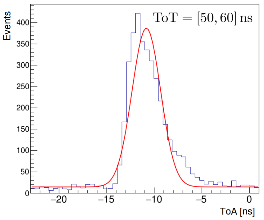
Given that with irradiation similar performance improvements are not present in the laser and calibration circuit measurements, the underlying cause of this effect cannot be a consequence of the pixel electronics or signal processing, but rather of the charge carrier creation and collection processes specific to . Since the pixel is biased from the top of the chip (see pixel cross section in [18]), this results in curved electric field lines and low field regions near the border of the depletion region, where charge collection is presumed to be slow. This is confirmed by Backside-TCT results in figure 9, where charge created on the edge of the pixel (corresponding to lower values in the in-pixel scan) produces signals with a larger delay than the same amount of charge created in the pixel center, where collection is most efficient. The average value of these delays can be up to a couple of \unit, consistent with observations in figure 14(a). In addition, since the pixel is not fully depleted at a bias voltage of , some amount of charge created in the undepleted bulk reaches the depletion region via diffusion, subsequently being collected on the electrode and contributing to the induced signal. Since these delayed events cannot be filtered out in the measurements, they contribute to the time resolution calculation and worsen the results. After irradiation, the charge carrier lifetime decreases due to deep energy levels accelerating the charge carrier recombination [26]. As a result, less charge from the slower component is able to reach the depleted region [27] and produce a delayed pixel response, thus essentially eliminating the delayed events in the bin distributions of the irradiated sample (figure 14(b)) and improving the time resolution.
4 Conclusion
Timing properties were determined for active pixels of the RD50-MPW2 monolithic prototype detector manufactured in HV-CMOS technology. Measurements at bias voltage with typical chip configuration and threshold settings, and at deposited charge amounts close to those of MIPs, show a minimum time resolution of approximately measured with Backside-TCT and with Edge-TCT. Position sensitive scans in both orientations indicate a uniform performance across the central pixel volume with worse performance on the edges due to charge sharing and less efficient collection. No significant performance differences were seen with the TCT method when measuring a sample irradiated to \fluence. Measurements done with give a worse time resolution of around for the unirradiated sample, which was attributed to events where charge is deposited on the outermost parts of the pixel and charge collection is prolonged. Since charge carriers recombine faster after irradiation, less delayed events are able to produce a pixel response, thus improving the resolution.
Within the scope of characterizing the RD50-MPW2’s timing performance, the TCT method was utilized for the first time, both in Backside- and Edge-TCT configurations, to determine the time resolution of monolithic detectors. In comparison to or test beam campaigns, two commonly used methods, time resolution can be acquired with TCT in a shorter amount of time and, additionally, also provides an insight into timing performance with positional sensitivity on a sub-pixel level. Using TCT is therefore a suitable method for obtaining time resolution information quickly and in a relatively simple laboratory setting, giving it a promising future for applications in characterizing time resolution of monolithic particle detectors.
References
- [1] H.F.-W. Sadrozinski, A. Seiden and N. Cartiglia, 4D tracking with ultra-fast silicon detectors, Rep. Prog. Phys. 81 (2018) 026101.
- [2] I. Béjar Alonso, O. Brüning, P. Fessia, M. Lamont, L. Rossi, L. Tavian et al., eds., High-Luminosity Large Hadron Collider (HL-LHC): Technical design report, CERN Yellow Reports: Monographs, CERN, Geneva (2020), 10.23731/CYRM-2020-0010.
- [3] A. Abada, M. Abbrescia, S.S. AbdusSalam, I. Abdyukhanov, J. Abelleira Fernandez, A. Abramov et al., FCC-hh: The hadron collider, Eur. Phys. J. Spec. Top. 228 (2019) 755.
- [4] ATLAS Collaboration, Letter of intent for the Phase-II upgrade of the ATLAS experiment, Tech. Rep. CERN-LHCC-2012-022, LHCC-I-023, CERN, Geneva (2012).
- [5] ATLAS Collaboration, Technical design report: A High-Granularity Timing Detector for the ATLAS Phase-II upgrade, Tech. Rep. CERN-LHCC-2020-007, ATLAS-TDR-031, CERN, Geneva (2020).
- [6] C. Agapopoulou, S. Alderweireldt, S. Ali, M.K. Ayoub, D. Benchekroun, L. Castillo García et al., Performance in beam tests of irradiated low gain avalanche detectors for the ATLAS High Granularity Timing Detector, J. Instrum. 17 (2022) P09026.
- [7] C. Betancourt, D. De Simone, G. Kramberger, M. Manna, G. Pellegrini and N. Serra, Time resolution of an irradiated 3D silicon pixel detector, Instruments 6 (2022) 12.
- [8] G. Iacobucci, L. Paolozzi, P. Valerio, T. Moretti, F. Cadoux, R. Cardarelli et al., Efficiency and time resolution of monolithic silicon pixel detectors in SiGe BiCMOS technology, J. Instrum. 17 (2022) P02019.
- [9] I. Perić, A novel monolithic pixelated particle detector implemented in high-voltage CMOS technology, Nucl. Instrum. Methods Phys. Res. A 582 (2007) 876.
- [10] G. Kramberger, V. Cindro, I. Mandić, M. Mikuž, M. Milovanović, M. Zavrtanik et al., Investigation of irradiated silicon detectors by Edge-TCT, IEEE Trans. Nucl. Sci. 57 (2010) 2294.
- [11] C. Zhang, G. Casse, N. Massari, E. Vilella and J. Vossebeld, Development of RD50-MPW2: a high-speed monolithic HV-CMOS prototype chip within the CERN-RD50 collaboration, in PoS (TWEPP2019), vol. 370, p. 045, 2020, DOI.
- [12] E. Vilella, Development of high voltage-CMOS sensors within the CERN-RD50 collaboration, Nucl. Instrum. Methods Phys. Res. A 1034 (2022) 166826.
- [13] L. Snoj, G. Žerovnik and A. Trkov, Computational analysis of irradiation facilities at the JSI TRIGA reactor, Appl. Radiat. Isot. 70 (2012) 483.
- [14] K. Ambrožič, G. Žerovnik and L. Snoj, Computational analysis of the dose rates at JSI TRIGA reactor irradiation facilities, Appl. Radiat. Isot. 130 (2017) 140.
- [15] R. Marco Hernández, Latest depleted CMOS sensor developments in the CERN RD50 collaboration, in JPS Conf. Proc., vol. 34, p. 010008, 2021, DOI.
- [16] H. Liu, M. Benoit, H. Chen, K. Chen, F.A. Di Bello, G. Iacobucci et al., Development of a modular test system for the silicon sensor R&D of the ATLAS upgrade, J. Instrum. 12 (2017) P01008.
- [17] T. Vanat, Caribou – a versatile data acquisition system, PoS TWEPP2019 (2020) 100.
- [18] B. Hiti, V. Cindro, A. Gorišek, M. Franks, R. Marco-Hernández, G. Kramberger et al., Characterisation of analogue front end and time walk in CMOS active pixel sensor, J. Instrum. 16 (2021) P12020.
- [19] I. Mandić, V. Cindro, J. Debevc, A. Gorišek, B. Hiti, G. Kramberger et al., Study of neutron irradiation effects in depleted CMOS detector structures, J. Instrum. 17 (2022) P03030.
- [20] “Particulars, Advanced measurement systems, Ltd.” https://www.particulars.si/.
- [21] N. Cartiglia, M. Baselga, G. Dellacasa, S. Ely, V. Fadeyev, Z. Galloway et al., Performance of ultra-fast silicon detectors, J. Instrum. 9 (2014) C02001.
- [22] C. Tsolanta, Characterisation and time resolution measurements of the RD50-MPW2 monolithic silicon pixel sensor, Master’s thesis, University of Amsterdam, 2022, https://scripties.uba.uva.nl/search?id=record_50779.
- [23] G. Kramberger, V. Cindro, D. Flores, S. Hidalgo, B. Hiti, M. Manna et al., Timing performance of small cell 3D silicon detectors, Nucl. Instrum. Methods Phys. Res. A 934 (2019) 26.
- [24] G. Kramberger, V. Cindro, A. Howard, Ž. Kljun, I. Mandić and M. Mikuž, Annealing effects on operation of thin Low Gain Avalanche Detectors, J. Instrum. 15 (2020) P08017.
- [25] N. Cartiglia, A. Staiano, V. Sola, R. Arcidiacono, R. Cirio, F. Cenna et al., Beam test results of a 16 ps timing system based on ultra-fast silicon detectors, Nucl. Instrum. Methods Phys. Res. A 850 (2017) 83.
- [26] E. Gaubas, T. Ceponis, L. Deveikis, D. Meskauskaite, J. Pavlov, V. Rumbauskas et al., Anneal induced transformations of defects in hadron irradiated Si wafers and Schottky diodes, Mater. Sci. Semicond. Process. 75 (2018) 157.
- [27] G. Kramberger, Reasons for high charge collection efficiency of silicon detectors at HL-LHC fluences, Nucl. Instrum. Methods Phys. Res. A 924 (2019) 192.