Unidirectional Nano-Modulated Binding and Electron Scattering in Epitaxial Borophene
Abstract
A complex interplay between the crystal structure and electron behavior within borophene renders this material an intriguing 2D system with many of its electronic properties still undiscovered. Experimental insight into those properties is additionally hampered by the limited capabilities of the established synthesis methods, which in turn inhibits the realization of potential borophene applications. In this multi-method study, photoemission spectroscopies and scanning probe techniques complemented by theoretical calculations have been used to investigate the electronic characteristics of a high-coverage, single-layer borophene on Ir(111) substrate. Our results show that the binding of borophene to Ir(111) exhibits pronounced one-dimensional modulation and transforms borophene into a nano-grating. The scattering of photoelectrons from this structural grating gives rise to the replication of electronic bands. In addition, the binding modulation is reflected in the chemical reactivity of borophene and gives rise to its inhomogeneous aging effect. Such aging is easily reset by dissolving boron atoms in iridium at high temperature followed by their reassembly into a fresh atomically-thin borophene mesh. Besides proving electron-grating capabilities of the boron monolayer, our data provides a comprehensive insight into the electronic properties of epitaxial borophene which is vital for further examination of other boron systems of reduced dimensionality.
I Introduction
Synthesis of various borophene (Bo) polymorphs on a range of different substrates (Li et al., 2023) opened new pathways for investigation of these atomically-thin boron systems. In order to attain precise control over the synthesis, growth of Bo is typically carried out in ultra-high vacuum (UHV) conditions on metallic single-crystals. In such way, epitaxial Bo has been realized on Ag, Cu, Ir, Au, Al and Ru substrates (Feng et al., 2016a; Wu et al., 2019; Vinogradov et al., 2019; Kiraly et al., 2019; Li et al., 2018a; Sutter and Sutter, 2021). Epitaxial growth holds potential for high sample quality – in terms of size, number of defects and structural homogeneity – which is often an imperative for investigation of intrinsic properties of Bo. Also, high material quality is required for various technological applications of Bo, such as metal-ion batteries (Zhang et al., 2016; Yu et al., 2022), supercapacitors (Li et al., 2018b), hydrogen storage (Er et al., 2009), gas sensors (Huang et al., 2018) and freshwater production (Guan et al., 2023).
However, binding to the metal substrate is reflected in the structural and physical properties of epitaxial Bo. Interaction of Bo with the underlying metal not only defines the most stable polymorph (Zhang et al., 2015), but can also induce new morphology in the form of stripes, chains and zig-zag arrays which are identified as the moiré patterns in some cases (Feng et al., 2016a; Wu et al., 2019; Liu et al., 2019; Kiraly et al., 2019; Wang et al., 2020). All these nanoscopic structures are in turn linked to the electronic and vibrational properties of Bo, and are expected to perturb intrinsic features of Bo such as high electrical and thermal conductivity (Adamska et al., 2018; Zhou et al., 2017). Signatures of nano-modulation in other epitaxial two-dimensional (2D) systems can readily be found in the spectroscopic data, namely the valence band and the core-level electronic structure. Examples of this are Dirac cone replication of graphene on Ir(111) (Pletikosić et al., 2009) or distinct peaks in the N spectra of hexagonal boron nitride (hBN) on transition metals (Preobrajenski et al., 2007). However, experimental detection of similar signatures in Bo samples is only scarcely addressed in the literature.
In particular, studies employing angle-resolved photoemission spectroscopy (ARPES), the best tool for studying the valence band structure of materials, are largely lacking. ARPES has been employed in only a few Bo investigations due to the experimental challenges arising from the sample inhomogeneity (e.g. presence of several polymorphs, small domains, defects) and significant chemical reactivity of Bo. Up to now, only and polymorphs on Ag(111) have been examined with ARPES by Feng and co-workers, where metallicity and the existence of the Dirac cones have been suggested (Feng et al., 2016b, 2017, 2018). This limited set of data, especially considering a large number of other realizable polymorphs, leaves many open questions related to the repercussions of Bo nano-modulation on its electronic properties and performance in electronic devices.
Here we report a combined experimental and computational study of Bo on Ir(111) (Bo/Ir) with a focus on the electronic properties governed by the nanoscopic modulation of the boron sheet. X-ray photoelectron spectroscopy (XPS) and scanning tunneling spectroscopy (STS) data show clear evidence of inhomogeneous binding of Bo to Ir, which results in a stripe-like structure of Bo. This structure in turn effectively produces a one-dimensional (1D) grating, giving rise to the umklapp scattering of photoelectrons which are detected in ARPES experiments. Density functional theory (DFT) calculations support our experimental findings and give an additional insight into the pristine electronic structure of Bo, void of nanoscopic modulation imprinted by the presence of the Ir substrate.
II Results
II.1 Evolution of the Ir and B core-levels
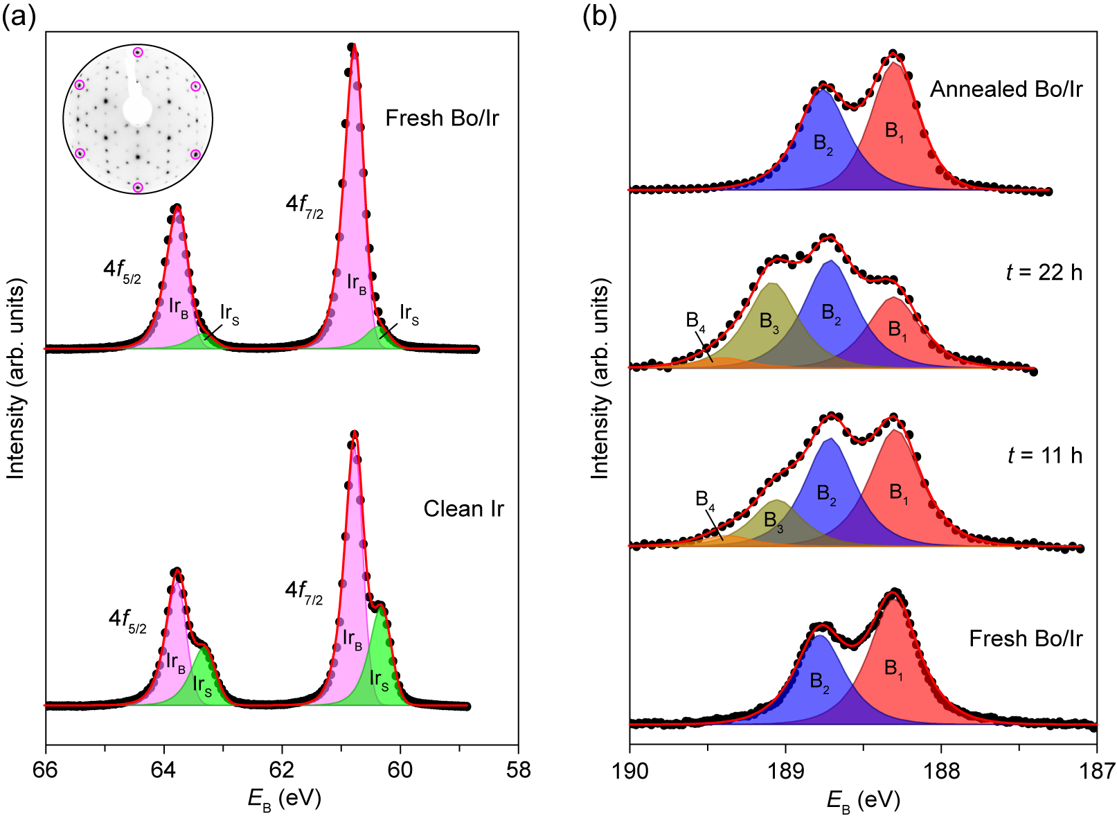
Prior to Bo synthesis, a reference Ir core-level photoemission spectrum has been recorded as shown in Fig. 1(a) bottom. Surface (IrS) and bulk (IrB) components of the Ir peaks are discerned with binding energies () of 60.33 and 60.80 eV (Ir ), and 63.33 and 63.80 eV (Ir ), respectively, in agreement with the literature data (Varykhalov et al., 2012). The intensity ratio of surface to bulk components, at the utilized photon energy of 300 eV, is 0.38 for Ir and 0.42 for Ir .
Bo synthesis consisted of B uptake in the Ir bulk during exposure of hot Ir crystal to the borazine vapors, followed by sample cooling which resulted in segregation of B atoms to the surface and their self-assembly into a Bo mesh (see Methods for further details) (Omambac et al., 2021). Successful Bo synthesis was firstly confirmed by LEED, where a characteristic pattern in three rotational domains was found [see Fig. 1(a) inset], designating the presence of the polymorph on the sample surface. Comparable intensities of Ir and Bo diffraction spots are an indication of relatively high Bo coverage (Radatović et al., 2022). The respective Ir core level spectra of Bo/Ir is shown in Fig. 1(a) top. In order to get a reliable fit, both IrS and IrB components must be included in the fitting procedure. The binding energies of all components remain the same as before Bo synthesis, but the ratios reduce significantly (by a factor ) for both the Ir and the Ir components.
Apparently, the presence of Bo on top of Ir surface suppresses the surface component of the Ir level. This indicates significant interaction between the Bo polymorph and Ir(111), since a similar reduction of the IrS peak is detected after adsorption of strongly bound species to the Ir surface (Bianchi et al., 2009; Baronio et al., 2022). In contrast, for weakly interacting epitaxial layers, such as graphene or hBN on Ir(111) (Varykhalov et al., 2012; Farwick zum Hagen et al., 2016), the surface component is almost unaltered in the presence of the 2D overlayer. Possible origin of the relatively small surface component which persists in our sample could be in the fraction of the Ir surface which is left uncovered after the Bo synthesis, considering recent micro-spot XPS examination of Bo/Ir where only bulk Ir peaks have been detected (Jugovac et al., 2023).
B spectrum of the Bo/Ir(111) sample recorded immediately after Bo synthesis is shown in Fig. 1(b) bottom. Two distinct components are visible, labeled B1 and B2, located at of 188.30 and 188.78 eV. The intensity ratio of the two components is . For the freshly synthesized Bo samples, no other B-related peaks were observed. Also, no signatures were found of additional B peaks at higher binding energies, characteristic for hBN layers (Orlando et al., 2012).
The B energy region has been monitored via XPS over an extended period of time during which the sample was left in the UHV chamber at a base pressure in the 10-10 mbar range. As shown in Fig. 1(b) for samples 11 and 22 hours after the synthesis, we observed modifications of the initial B1 and B2 peaks as well as the appearance of additional peaks. The B1 peak remains at the same energy but loses intensity as the time progresses. The B2 peak shows a different behavior – it maintains an almost constant intensity but slightly shifts, by meV, to lower binding energies. After 22 hours, the ratio decreases to 0.65. The reduction of the B1 peak intensity is accompanied by the emergence of B3 and B4 components at 189.07 eV and 189.37 eV, respectively. These modifications of the B peak are attributed to binding of residual C- and/or O-containing molecules from the UHV environment to boron atoms (Moddeman et al., 1989; Ong et al., 2004; Cattelan et al., 2013). Based on the B 1 peak intensities, we conclude that after 22 hours in UHV these molecules bind to approximately of boron atoms within Bo. Significant chemical reactivity of Bo sheets contrasts chemical inertness of boron-containing hBN which shows no contamination signatures in XPS data even after prolonged exposure to air (Kidambi et al., 2014). It was demonstrated that exactly such inertness of hBN, as well as that of graphene, can be utilized for protecting Bo from contamination by synthesizing hBN/Bo and graphene/Bo vertical heterostructures (Cuxart et al., 2021; Jugovac et al., 2023).
In the follow-up control experiment, the sample was flashed to 1100 °C and immediately cooled down, in order to dissolve boron in Ir, desorb any contaminants from the sample surface and produce a fresh Bo layer via B segregation to the Ir surface (see Supporting Figure S1). Such procedure is a straightforward route for obtaining pristine samples, relying on the temperature-dependent solubility of B in Ir that was already exploited in previous studies (Omambac et al., 2021, 2023). Indeed, the XPS spectrum of the annealed sample shown in Fig. 1(b) top looks essentially the same as the spectrum of the initial, pristine Bo/Ir sample, exhibiting only B1 and B2 components with restored positions and intensities. In addition, LEED data exhibiting a sharp pattern in three domains (not shown) confirmed the presence of a clean Bo layer.
II.2 Valence band structure
In order to identify any new valence band features related to Bo, we first examined the Fermi surface of a freshly prepared sample via spatially-averaging ARPES where the spot size on the sample surface had a diameter of mm. Besides the rich band structure characteristic of the Ir(111) surface, new prominent arc-like features are found close to the surface Brillouin zone (SBZ) center, marked by white arrows (i.e. wavevectors , to be elaborated below) in Fig. 2(a). A detailed comparison of clean Ir and Bo/Ir ARPES data is given in the Supporting Figure S2. These arcs exhibit anisotropic intensity and an overall 3-fold symmetric arrangement in the -space. The energy dispersion of the arcs in -M and -K directions is disclosed in Fig. 2(b) where a linear dispersion is identified extending down to eV.
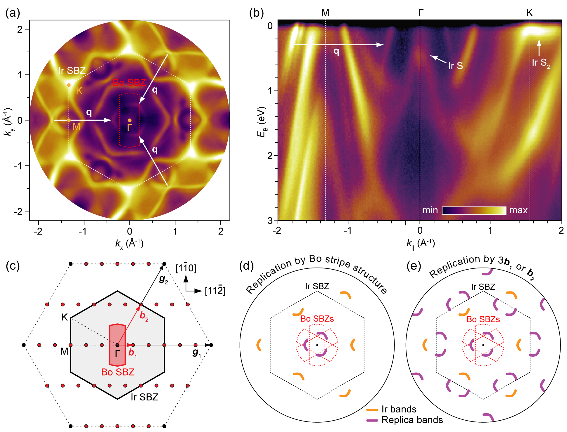
The Bo-induced bands are situated outside of the first SBZ of Bo and the shape of the arcs does not reflect the expected shape imposed by the symmetry of SBZs of Bo, which indicates that they are actually not electronic bands of the Bo itself. By taking into account the corrugated morphology of Bo on Ir(111) (Vinogradov et al., 2019; Omambac et al., 2021), it is plausible that the observed bands are replicated (i.e., umklapp) bands of Ir. A similar band replication has been observed before in other 2D material systems, e.g. for silicene on Ag(111) (Sheverdyaeva et al., 2017) and TaS on Au(111) (Dombrowski et al., 2021). Indeed, a careful inspection of the data from Fig. 2(a) and (b) allows identification of the Ir bands with the same Fermi contours and band dispersions as the Bo-induced bands. The tendency of these particular Ir bands to undergo replication might be correlated with their significant surface localization (Bornemann et al., 2012; Dal Corso, 2015). The corresponding replication wavevectors are noted in Fig. 2(a) and (b) where they point from the original bands to the replica bands. For the clarity of data representation, we choose bands outside of the first SBZ of Ir as bands being replicated, whereas the same bands can be found inside of the first SBZ due to -space periodicity. Schematic of the electronic bands involved in the replication is shown in Fig. 2(d). The wavevectors are parallel to the -M directions (i.e. directions) and have a magnitude of Å-1. As will be shown later, is closely related to the specific structure of Bo on Ir. Therefore, we identify the bands marked by white wavevectors in Fig. 2(a) and (b) as replicas of the Ir bands.
The replica bands persist in UHV conditions, essentially unchanged in position and intensity for up to 10 hours after the sample synthesis when significant chemical modifications already occur in Bo [cf. Fig. 1(b)]. This additionally supports the replication scenario, since chemical modification of Bo is expected to also leave an imprint on its valence band structure. Further details about band replication process will be given in the Discussion.
As already mentioned, the surface states of Ir are visible in the ARPES data in Fig. 2(b) (see arrows labeled Ir S1 and Ir S2) (Pletikosić et al., 2010). The state at the point, having an offset from , is more suitable for further quantitative analysis. We find that the energy of the surface state remains the same after Bo formation, but its intensity is reduced and the corresponding linewidth becomes larger, indicating reduction of the coherency of the surface state [see Supporting Figure S3(a)]. Even though contributions of the uncovered Ir surface to these effects cannot be excluded, it is also plausible that Bo has a specific impact on the surface state, as will be elaborated below.
Spatially-resolved insight into the valence band structure of Bo on Ir has been gained from ARPES measurements which complement conventional (i.e. spatially-averaging) ARPES data. Fig. 3(a) shows a representative area of the sample which has been deliberately prepared with submonolayer Bo coverage for the purpose of these measurements. Terrace-filling patterns, where a single terrace is most often filled by a single Bo domain, are clearly resolved which is characteristic for segregation-assisted growth of Bo on Ir(111) (Omambac et al., 2021). Typical width of the terraces and thus individual Bo domains was of the order of 1 m or less, which prevented probing of a single Bo domain with ARPES (having probing area diameter of m). The presence of Bo on the surface is easily identified in LEED by a characteristic pattern [see Fig. 3(b)]. Uncovered Ir and Bo/Ir regions were targeted in ARPES measurements.
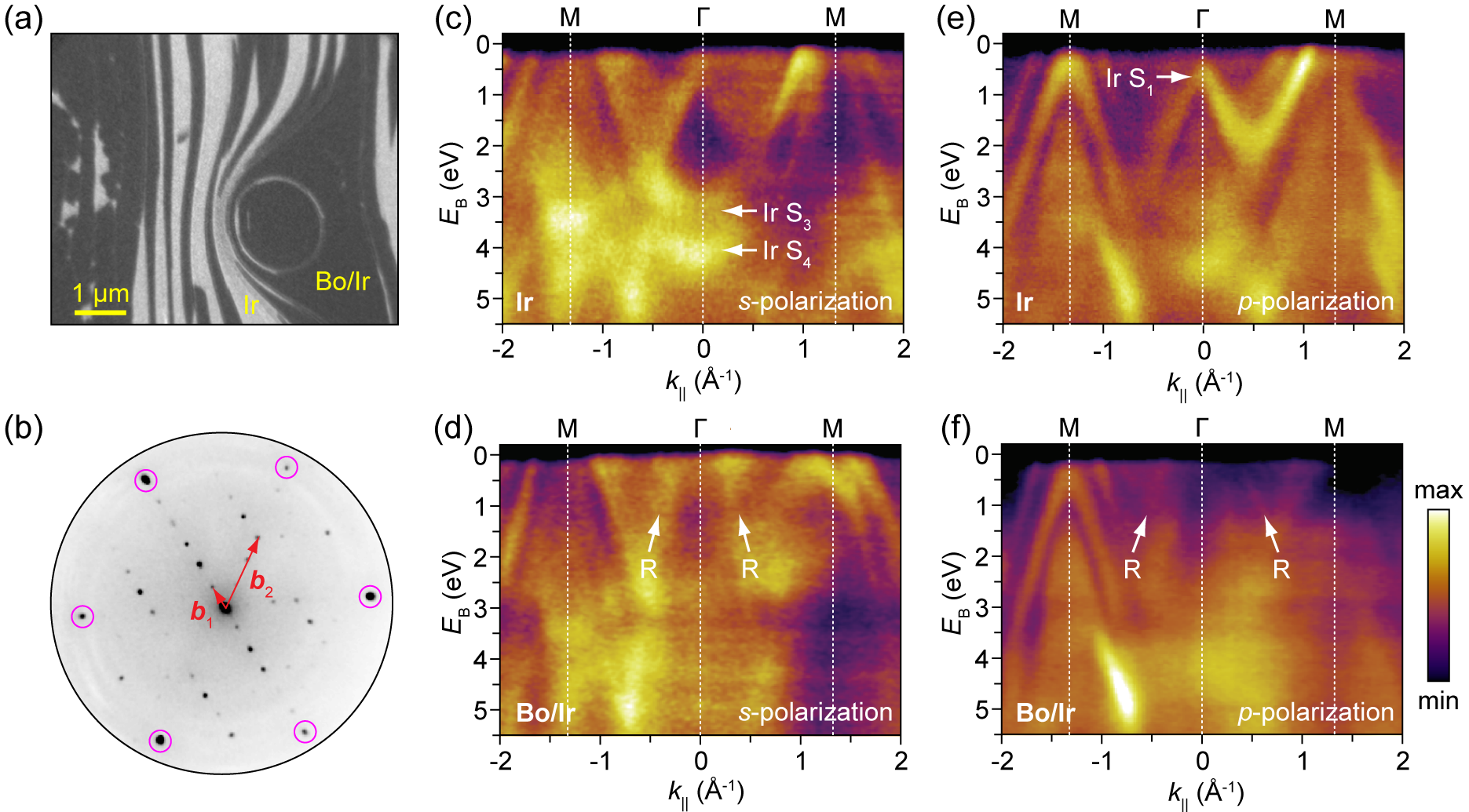
The corresponding valence band structures are displayed in Fig. 3(c-f). By utilizing both and polarized light, the Ir replica bands can be identified in the Bo/Ir spectra which are absent in the case of uncovered Ir surface. The iridium surface state at the point Ir S1 is significantly suppressed under the Bo layer and is almost invisible at the employed photon energy and spectral resolution. Similar observation can be made for two other states Ir S3 and Ir S4 which exhibit significant localization in the top surface layers of iridium (Dal Corso, 2015). In the spectrum in Fig. 3(f), where polarization of light has been used, a subtle increase of the photoemission intensity is visible in the vicinity of the point, in the range eV [see also Supporting Figure S3(b)]. We speculate that this signal can be attributed to traces of the Bo band identified recently for graphene-capped Bo sample (Jugovac et al., 2023), which must have orbital character since it is invisible while utilizing polarized photons.
ARPES measurements also allow the detection of secondary electron cut-off and the determination of the work function of the sample. It is found that the work function of Bo/Ir is eV, which is less than the work function of clean Ir(111) surface eV (Derry et al., 2015). Such work function reduction can be assigned to hole doping of Bo, i.e. net electronic charge transfer from Bo to Ir, similar as for graphene on metals (Khomyakov et al., 2009). Even though marginal hole doping of Bo on Ir(111) has been theoretically predicted (Vinogradov et al., 2019), we note that our work function data has been recorded 4 hours after the Bo synthesis, when already different adsorbates from the UHV could have affected the work function value of Bo/Ir. For comparison, electron doping of Bo (accompanied by an increase of the work function) has been measured for and polymorphs on Ag(111) (Liu et al., 2021), which demonstrates the influence of the substrate material (and the respective binding) on the charge rearrangement in epitaxial Bo layers.
II.3 Microscopy and spectroscopy at the nanoscale
Further details of the electronic structure of Bo/Ir at the atomic level are obtained from STM and STS measurement. A typical STM image of the system is shown in Fig. 4(a), with a characteristic stripe-like pattern of the Bo polymorph. The stripes of width Å run diagonally across the figure panel and appear to be separated by trenches. Additionally, each stripe consists of two parallel rows of lobes, thus constituting two “wavy” sub-stripes (Vinogradov et al., 2019; Omambac et al., 2021; Cuxart et al., 2021). For comparison, top-right corner of Fig. 4(a) depicts the appearance of freestanding Bo as calculated by DFT. In that case, the stripe-like pattern is absent, which demonstrates that it is imprinted in the Bo/Ir system by the Ir substrate. In order to investigate the contribution of the electronic structure to such appearance of Bo on Ir(111), STS measurements were carried out.
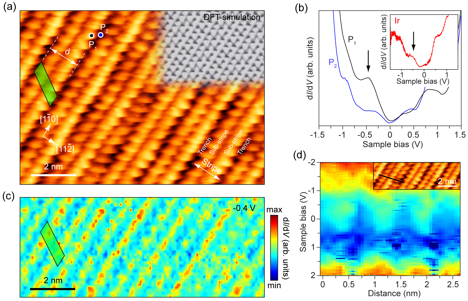
Fig. 4(b) shows two point spectra, recorded at the lobe (P1) and trench (P2) positions. Both spectra are V-shaped in the vicinity of which is a signature of metallicity of Bo/Ir. However, there is a notable difference between the two spectra in the energy range between 0.3 and 0.5 eV below . The spectrum at the lobe position contains a significantly higher density of states (DOS) in comparison to the spectrum at the trench position [see arrow in Fig. 4(b)]. The same state was observed for the bare Ir(111) surface [see inset of Fig. 4(b)] and can be assigned to the surface state Ir S1 located at the point (Schulz et al., 2014). Therefore, our data indicates that the surface state persists under the Bo sheet, although with spatially-modulated intensity – the state is suppressed in the trenches but is pronounced in the lobes of the Bo’s stripe-like structure.
Such spatial modulation of the Ir surface state is even better visualized in the STS map and line scan, shown in Fig. 4(c) and (d). The STS map recorded at -0.4 V of bias voltage displays clear coincidence with the topographic image from panel (a). This coincidence is evidence of a link between Bo crystal structure and Ir surface state coherence, which in turn points towards inhomogeneous binding of Bo to Ir at the nanoscale. Such modulation of the Ir surface state also explains its spectral modifications in our ARPES data.
II.4 Electronic structure from DFT calculations
DFT calculations of the electronic properties of freestanding Bo polymorph have been carried out. In this way we complement our experimental data, in particular our ARPES and XPS findings, and provide additional support to the nano-modulated nature of the Bo/Ir system. Prior to the electronic structure calculation, the B atom positions were relaxed in order to reach optimized crystal structure [see Fig. 5(a) inset]. The simulated XPS spectrum of the B peak of such an optimized structure is shown in Fig. 5(a). The spectrum essentially consists of two peaks, corresponding to five 4- (B4C) and twenty 5-coordinated (B5C) atoms. These two peaks are centered at 187 eV and 187.7 eV binding energy, respectively. Altogether, the two peaks merge into one dominant peak with a shoulder on the low binding energy side.
A fit to the experimental XPS data from Fig. 1(b)-bottom is also overlapped in Fig. 5(a) as a dashed line. Apparently, neither do the peak separation nor the peak intensity ratio match the calculated expectations, which points towards nano-modulation as a possible source of inhomogeneous Bo-Ir interaction. A shift of the calculated spectrum towards lower binding energies with respect to the experimental data is explained by the absence of the substrate in our theoretical calculations.
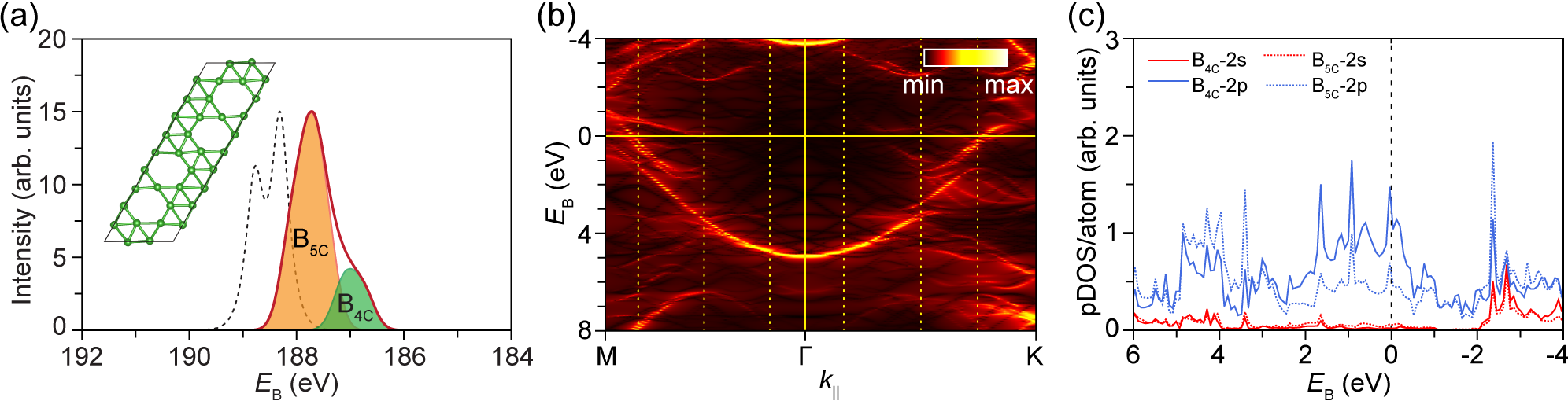
The calculated band dispersion is plotted in Fig. 5(b), unfolded to the first SBZ of Ir(111) for a better overview. An average of three 120°-rotated Bo domains is shown, thus mimicking area-averaging of the conventional ARPES measurements (single-domain calculated bands are shown in Supporting Figure S4). The most dominant feature is a parabolic band with the vertex at eV. Notably, there are no pronounced electronic bands close to around the point (and in particular, with a large velocity) which could be identified as the Bo-induced bands from our ARPES measurements, further confirming Ir band replication scenario. The corresponding projected density of states (pDOS) is plotted in Fig. 5(c). It is clear that Bo bands are dominantly of character, for both 4- and 5-coordinated B atoms. Published calculations of other Bo polymorphs ( and ) show similarity to these results, most notably in respect to the orbital symmetry and binding energy of the character bands centered at the point (Penev et al., 2016; Abbasi et al., 2023). The calculated work function of a freestanding Bo layer is = 4.86 eV.
III Discussion
Let us first clarify the origin of the B1 and B2 peaks found in the XPS spectra of a fresh Bo/Ir sample. Considering all of our data, we conclude that the two B peaks arise from distinct registries and inhomogeneous binding of B atoms with respect to the substrate atoms, similar as for hBN on Ir(111) and on other metallic substrates as well (Orlando et al., 2012; Preobrajenski et al., 2007). In our case, B atoms located in the lobes and trenches exhibit notably different interaction with Ir, in agreement with the STS data in Fig. 4, which is then reflected in two distinct B levels. In analogy with the hBN/Ir(111) system (Orlando et al., 2012), it is plausible that the lower binding energy component B1 corresponds to B atoms located in the weakly bound lobes. Those B atoms readily react with residual molecules from UHV [cf. Fig. 1(b)]. The higher binding energy component B2 originates from B atoms strongly bound to Ir within the trenches of the Bo structure and they are somewhat more robust against “rapid” adsorption of molecules from the UHV. Similar assignment of the two B peaks, separated by eV, was assumed before for buckled Bo on Ag(111) (Mannix et al., 2015). Therefore, B-Ir interaction exhibits nano-modulation and in parallel induces spatially-varying chemical reactivity of Bo from the top (i.e., vacuum) side. In addition, inhomogeneous B-Ir interaction induces the stripy structure of Bo, as also supported by the simulated STM image of a freestanding Bo [inset in Fig. 4(a)].
Other factors, such as coordination of B atoms with other B neighbors, cannot be the reason for the double-peaked B structure primarily since this effect should yield , in line with our DFT calculations in Fig. 5(a), which is far from the measured experimental ratio. Even though the intrinsic coordination effect may exist, we presume that it is obscured in our data by the establishment of B-Ir bonds and dominance of the nonuniform Bo-Ir interaction described above. Also, we eliminate B atoms still embedded in Ir (sub)surface as potential origin of the B double-peak structure, as in the case of Bo on Al(111) (Preobrajenski et al., 2021). This scenario is unlikely since both B1 and B2 disappear upon Bo oxidation in ambient conditions (Jugovac et al., 2023), whereas at least one component (corresponding to the alloy) should remain protected. Also, we found no evidence of a new Ir peak which would signify the presence of B-Ir alloy, as in the case of favorable Si-Ir intermixing over silicene formation (Satta et al., 2018). Contributions from other Bo polymorphs on the sample surface to the double-peak B structure are excluded based on our STM, LEEM and LEED data.
Besides an evident modulation of the B-Ir interaction at the nanoscale, we can also qualitatively assess B-Ir binding from our XPS, ARPES and STS data. The reduction of the iridium core-level component IrS [Fig. 1(a)] and the suppression of the Ir surface state Ir S1 [Fig. 2, Fig. 3 and Supporting Figure S3] signify a rather strong B-Ir interaction. However, the state Ir S1 is not completely quenched under the Bo layer (Fig. 4), which would altogether categorize the B-Ir interaction as moderate. Moderate interaction is in line with the ability of room temperature intercalation of gold atoms underneath Bo on Ir(111) (Vinogradov et al., 2019). Interestingly, the surface state of Ag was quenched under the Bo layer (Liu and Hersam, 2019), which might indicate stronger binding of Bo to Ag(111) as compared to Ir(111).
Investigation of the valence band structure of Bo is hindered by substantial chemical (re)activity of Bo even in UHV conditions (cf. Fig. 1). Additionally, the rich electronic structure of Ir obscures (and potentially hybridizes with) any band which does not fall into one of Ir’s bandgaps (Pletikosić et al., 2010). In this study, clearly visible new features arising from the Bo presence on the sample surface are Ir replica bands. Opening of electronic gaps in their vicinity has not been observed (as opposed to graphene on Ir(111) (Pletikosić et al., 2009)), which confirms their umklapp origin and also final-state-effect character. Considering the common sources of such band replication, one can assume that the reciprocal lattice of Bo is the source of electron scattering. It can be immediately recognized that the replication wavevector matches (both in direction and magnitude) the reciprocal vectors or of the three Bo domains [see Fig. 2(c)], since Å-1 where Å is the surface lattice constant of Ir(111) (Arblaster, 2010). However, if either or vectors alone would cause the umklapp scattering, the number of the replicated bands in ARPES data should be rather large, as depicted in Fig. 2(e) (see Supporting Figure S5 for additional details). Since this situation does not correspond to our ARPES measurements, some other factors must be involved in the electron scattering process.
A reasonable assumption is that the stripe-like structure of Bo can affect electron scattering, since it introduces an additional periodicity in the system. If only scattering of electrons with momentum perpendicular to the Bo stripes is taken into account, the number of replicas is significantly reduced. The expected replica arrangement in that case is schematically shown in Fig. 2(d), which is in agreement with our experimental measurements. Therefore, umklapp process is not induced by the wavevectors or , but rather by the stripy structure of Bo which constitutes a 1D lattice with a wavevector . Scattering is happening only in the direction perpendicular to the Bo stripes, i.e. only for the electrons moving along directions. Similar 1D-only umklapp processes have been identified previously for graphene nanoribbons on Ni(771) (Shikin et al., 2003), and graphene sheets on Pt(997) (Pisarra et al., 2014) and reconstructed Au(001) (Terasawa et al., 2023). To the best of our knowledge, band replication induced by atomically thin boron layers has not been reported before. Despite the electron scattering on Bo stripe structure, the relation still holds, meaning that the corresponding diffraction spots in the LEED data (stripe-related and lattice-related) cannot be distinguished.
The replication vector translates into a real-space periodicity of Å. This value coincides with , i.e. one third of the Bo stripe width. In the STM and STS data in Fig. 4, this periodicity can be recognized as a characteristic lengthscale of Ir topography and surface state modulation in the direction perpendicular to Bo stripes, thus being closely related to the sub-stripes. Therefore, unidirectional nano-scale modulation of the Bo-Ir binding perturbs Bo lattice in a way to yield a 1D stripy structure – i.e. an atomically-thin diffraction grating – with a wavevector as the dominant scattering component.
IV Conclusions
In a combined experimental and theoretical approach, we investigated the structural and electronic properties of an extended borophene (Bo) monolayer on the (111) surface of Ir. Significant nanoscopic and unidirectional modulation of Bo is found, arising form nonuniform interaction of B atoms with the underlying Ir atoms. Such modulation results in a stripe-like structure of Bo, which in turn acts as an electron diffraction grating. Electron diffraction (i.e. scattering) is manifested in the form of replica bands which have been detected in the photoemission spectra of the Bo/Ir system in the vicinity of the Fermi level. The pristine structure of this atomically-thin boron grating, being chemically (re)active and prone to atomic-scale modifications, can be easily restored by executing a dissolution-segregation cycle during which B atoms reassemble into a fresh Bo mesh.
Our results showcase scattering capabilities of 2D materials and stimulate further examination of other Bo polymorphs which might exhibit different types of superperiodicity phenomena. The presented data constitute a comprehensive insight into the electronic structure of epitaxial Bo which is vital for further development of Bo-based applications. In addition, our work demonstrates facile fabrication of a nanoscopic, highly-ordered system which may serve as a template for further functionalization and also become a building block in more complex 2D-based heterostructures and devices with enhanced electronic properties.
V Methods
V.1 Sample preparation
Bo samples were synthesized in four ultra-high vacuum (UHV) systems on an Ir(111) single-crystal (see below for details of these systems), and sample preparation procedure was the same in all of them, with minor differences which yielded the same end result. Ir substrate cleaning consisted of argon or xenon sputtering at keV followed by heating in oxygen atmosphere at °C and annealing at °C. The surface quality was checked by sharp low-energy electron diffraction (LEED) spots of Ir, presence of the Ir surface states as well as absence of contamination-related peaks in XPS (where applicable). For Bo synthesis, boron dissolution-segregation method was used (Omambac et al., 2021; Radatović et al., 2022), during which the Ir surface was repeatedly exposed to borazine at a pressure in the range mbar and temperature of °C, and subsequently cooled to room temperature. Sample heating was realized via e-beam bombardment (with typical heating rates in the 15-20 °C/s range) while cooling was achieved by switching off the e-beam source (with typical cooling rates in the 3-10 °C/s range), without any additional active cooling mechanism. Sample preparation parameters used in different setups are given in the Supporting Table 1.
V.2 X-ray photoelectron spectroscopy (XPS)
XPS data were recorded in situ at the VUV-Photoemission beamline of the Elettra synchrotron (Trieste, Italy) at room temperature and in normal emission. A Scienta R4000 electron analyzer was used for data acquisition with the slit oriented parallel to the scattering plane of the experiment. Linearly polarized light illuminated the sample at 45° with respect to the analyzer axis, with the light spot diameter on the sample surface of mm. XPS peaks were fitted by combined Gaussian-Lorentzian functions and Shirley background. The binding energy scale was calibrated either by using Ir bulk peaks or the Fermi level.
V.3 Conventional angle-resolved photoemission spectroscopy (ARPES)
ARPES data were recorded in situ in two setups: the VUV-Photoemission beamline of the Elettra synchrotron (Trieste, Italy) and the UARPES (now URANOS) beamline of the Solaris synchrotron (Krakow, Poland). At VUV-Photoemission, data [Fig. 2, Supporting Figure S2(d-f) and Supporting Figure S3(a)] were recorded at the same conditions and geometry as described in the preceding (XPS) subsection. 4D data sets () were acquired by rotating the sample azimuthally and by applying symmetry operations to the data. At UARPES, data [Supporting Figure S2(a-c)] were recorded in situ and at room temperature by employing the Scienta DA30L electron analyzer. Linearly polarized light illuminated the sample at 44° with respect to the analyzer axis, with the light spot diameter on the surface of mm. 4D data sets () were acquired by exploiting the full acceptance cone of the analyzer, i.e. no sample movement was necessary.
V.4 Micro-spot angle-resolved photoemission spectroscopy (ARPES)
ARPES measurements were performed in situ at the Nanospectroscopy beamline of the Elettra synchrotron (Trieste, Italy) with the SPELEEM III microscope (Elmitec GmbH) equipped with a hemispherical analyzer (Elmitec R200) and a 2D detector comprising a phosphorous screen and a CCD camera (QImaging Retiga). The sample was either illuminated with low-energy electrons (LEEM and LEED mode) or photons (ARPES mode). By inserting apertures in the illumination or imaging column of the microscope, characterization of the crystallography and electronic structure on the micrometer scale becomes available (LEED and ARPES, probing area of m in diameter). The electron energy is set by applying a voltage bias to the sample, commonly referred to as start voltage ().
V.5 Scanning tunneling microscopy and spectroscopy (STM and STS)
STM/STS measurements were carried out in situ at room temperature in a home-built system “Athene” at the University of Cologne, Germany. The curves were acquired by numerically differentiating single-point spectra, captured in 128×128 point grids. The processing of STM images (background subtraction, contrast enhancement) was done with the WSxM software (Horcas et al., 2007).
V.6 Density functional theory (DFT) calculations
We performed first-principles calculations based on DFT as implemented in the OpenMX code (Ozaki, 2003). The exchange-correlation effect in electrons was addressed by the generalized gradient approximation (Perdew et al., 1996). Each B atom had a pseudoatomic-orbital basis set with 7.0 bohr cutoff radius. By setting the bulk Ir lattice constant to 3.877 Å, we utilized a slab model for the free-standing borophene, whose in-plane lattice parameter was fixed to the Ir(111) lattice. The distance between slabs was 12 Å. In the geometry optimization, hartree and hartree/bohr of the total-energy and force-convergence criteria were utilized, respectively. The -centered grid was adopted. The core-hole pseudopotential on B , with the addition of a penalty-functional and Coulomb-cutoff approach as proposed by Ozaki et al. (Ozaki and Lee, 2017), was used for the calculations of the core-level excitation. To minimize the artificial interaction between core holes, the supercell corresponding to the Ir(111) lattice was incorporated into calculations. Within the Tersoff-Hamann approach, simulations of the STM images were carried out for an energy window between the Fermi level and -0.5 eV from it (Tersoff and Hamann, 1985; Horcas et al., 2007). For the band-structure unfoldings to the Ir(111) first SBZ (Wang et al., 2021), the projector-augmented wave method was utilized as implemented in the VASP code (Blöchl, 1994; Kresse and Furthmüller, 1996; Kresse and Joubert, 1999).
Supporting information
The supporting information is available free of charge at https://pubs.acs.org/doi/10.1021/acsami.3c14884. LEEM data sequence of borophene dissolution and recondensation, additional ARPES data of clean Ir and Bo/Ir samples, energy distribution cuts (EDCs) at the point before and after Bo formation, band dispersions of freestanding Bo in different high-symmetry directions as calculated by DFT, detailed schematics of the Fermi surface for different scattering scenarios, table of experimental parameters used for sample preparation.
Author contributions
S.K., P.M., P.M.S., A.V.M., M.K., and M.P. performed ARPES and XPS experiments. S.K., I.Š.J. and M.P. analyzed the ARPES and XPS data. M.J., C.A.B., T.O.M. and A.L. conducted ARPES and LEEM measurements and analyzed the respective data. I.S. and Y.G. executed and interpreted DFT calculations. P.B. and T.M. conducted and interpreted STM/STS experiments. All co-authors discussed the results. M.P. and S.K. prepared the manuscript with contributions from all co-authors. M.P. conceived and supervised research. All authors have given approval to the final version of the manuscript.
Acknowledgements.
This work was supported by the Croatian Science Foundation, Grant No. UIP-2020-02-1732 and by the Center of Excellence for Advanced Materials and Sensing Devices, ERDF Grant No. KK.01.1.1.01.0001. P.B. gratefully acknowledges financial support from the Alexander von Humboldt Foundation. T.M. acknowledges support by DFG within the project “Cluster Superlattice Membranes” (project No. 452340798). We acknowledge Elettra Sincrotrone Trieste for providing access to its synchrotron radiation facilities and for financial support under the IUS (P2022003) project. P.M., P.M.S. and A.V.M. acknowledge EUROFEL-ROADMAP ESFRI of the Italian Ministry of Education, University, and Research. This publication was developed under the provision of the Polish Ministry of Education and Science project: “Support for research and development with the use of research infrastructure of the National Synchrotron Radiation Centre SOLARIS” under contract No. 1/SOL/2021/2. We acknowledge SOLARIS Centre and in particular staff of the UARPES beamline for the access to the beamline and assistance during the measurements. The authors acknowledge the CERIC-ERIC Consortium for the access to experimental facilities and financial support. The calculations were partly carried out by using supercomputers at ISSP, The University of Tokyo, and TSUBAME, Tokyo Institute of Technology.References
- Li et al. (2023) W. Li, K. Wu, and L. Chen, Prog. Surf. Sci. 98, 100704 (2023).
- Feng et al. (2016a) B. Feng, J. Zhang, Q. Zhong, W. Li, S. Li, H. Li, P. Cheng, S. Meng, L. Chen, and K. Wu, Nat. Chem. 8, 563 (2016a).
- Wu et al. (2019) R. Wu, I. K. Drozdov, S. Eltinge, P. Zahl, S. Ismail-Beigi, I. Božović, and A. Gozar, Nat. Nanotechnol. 14, 44 (2019).
- Vinogradov et al. (2019) N. A. Vinogradov, A. Lyalin, T. Taketsugu, A. S. Vinogradov, and A. Preobrajenski, ACS Nano 13, 14511 (2019).
- Kiraly et al. (2019) B. Kiraly, X. Liu, L. Wang, Z. Zhang, A. J. Mannix, B. L. Fisher, B. I. Yakobson, M. C. Hersam, and N. P. Guisinger, ACS Nano 13, 3816 (2019).
- Li et al. (2018a) W. Li, L. Kong, C. Chen, J. Gou, S. Sheng, W. Zhang, H. Li, L. Chen, P. Cheng, and K. Wu, Science Bulletin 63, 282 (2018a).
- Sutter and Sutter (2021) P. Sutter and E. Sutter, Chem. Mater. 33, 8838 (2021).
- Zhang et al. (2016) X. Zhang, J. Hu, Y. Cheng, H. Y. Yang, Y. Yao, and S. A. Yang, Nanoscale 8, 15340 (2016).
- Yu et al. (2022) J. Yu, M. Zhou, M. Yang, Y. Zhang, B. Xu, X. Li, and H. Tao, Adv. Mater. Interfaces 9, 2102088 (2022).
- Li et al. (2018b) H. Li, L. Jing, W. Liu, J. Lin, R. Y. Tay, S. H. Tsang, and E. H. T. Teo, ACS Nano 12, 1262 (2018b).
- Er et al. (2009) S. Er, G. A. de Wijs, and G. Brocks, The J. Phys. Chem. C 113, 18962 (2009).
- Huang et al. (2018) C.-S. Huang, A. Murat, V. Babar, E. Montes, and U. Schwingenschlögl, The J. Phys. Chem. C 122, 14665 (2018).
- Guan et al. (2023) X. Guan, P. Kumar, Z. Li, T. K. A. Tran, S. Chahal, Z. Lei, C. Huang, C. Lin, J. Huang, L. Hu, Y. Chang, L. Wang, J. S. J. Britto, L. Panneerselvan, D. Chu, T. Wu, A. Karakoti, J. Yi, and A. Vinu, Adv. Sci. 10, 2205809 (2023).
- Zhang et al. (2015) Z. Zhang, Y. Yang, G. Gao, and B. I. Yakobson, Angew. Chem. Int. Ed. 54, 13022 (2015).
- Liu et al. (2019) X. Liu, L. Wang, S. Li, M. S. Rahn, B. I. Yakobson, and M. C. Hersam, Nat. Commun. 10, 1642 (2019).
- Wang et al. (2020) Y. Wang, L. Kong, C. Chen, P. Cheng, B. Feng, K. Wu, and L. Chen, Adv. Mater. 32, 2005128 (2020).
- Adamska et al. (2018) L. Adamska, S. Sadasivam, J. J. Foley, P. Darancet, and S. Sharifzadeh, The Journal of Physical Chemistry C 122, 4037 (2018).
- Zhou et al. (2017) H. Zhou, Y. Cai, G. Zhang, and Y. W. Zhang, npj 2D Materials and Applications 1, 1 (2017).
- Pletikosić et al. (2009) I. Pletikosić, M. Kralj, P. Pervan, R. Brako, J. Coraux, A. T. N’Diaye, C. Busse, and T. Michely, Phys. Rev. Lett. 102, 056808 (2009).
- Preobrajenski et al. (2007) A. Preobrajenski, M. Nesterov, M. L. Ng, A. Vinogradov, and N. Mårtensson, Chem. Phys. Lett. 446, 119 (2007).
- Feng et al. (2016b) B. Feng, J. Zhang, R.-Y. Liu, T. Iimori, C. Lian, H. Li, L. Chen, K. Wu, S. Meng, F. Komori, and I. Matsuda, Phys. Rev. B 94, 041408 (2016b).
- Feng et al. (2017) B. Feng, O. Sugino, R.-Y. Liu, J. Zhang, R. Yukawa, M. Kawamura, T. Iimori, H. Kim, Y. Hasegawa, H. Li, L. Chen, K. Wu, H. Kumigashira, F. Komori, T.-C. Chiang, S. Meng, and I. Matsuda, Phys. Rev. Lett. 118, 096401 (2017).
- Feng et al. (2018) B. Feng, J. Zhang, S. Ito, M. Arita, C. Cheng, L. Chen, K. Wu, F. Komori, O. Sugino, K. Miyamoto, T. Okuda, S. Meng, and I. Matsuda, Adv. Mater. 30, 1704025 (2018).
- Varykhalov et al. (2012) A. Varykhalov, D. Marchenko, M. R. Scholz, E. D. L. Rienks, T. K. Kim, G. Bihlmayer, J. Sánchez-Barriga, and O. Rader, Phys. Rev. Lett. 108, 066804 (2012).
- Omambac et al. (2021) K. M. Omambac, M. Petrović, P. Bampoulis, C. Brand, M. A. Kriegel, P. Dreher, D. Janoschka, U. Hagemann, N. Hartmann, P. Valerius, T. Michely, F. J. Meyer zu Heringdorf, and M. Horn-von Hoegen, ACS Nano 15, 7421 (2021).
- Radatović et al. (2022) B. Radatović, V. Jadriško, S. Kamal, M. Kralj, D. Novko, N. Vujičić, and M. Petrović, ACS Applied Materials and Interfaces 14, 21727 (2022).
- Bianchi et al. (2009) M. Bianchi, D. Cassese, A. Cavallin, R. Comin, F. Orlando, L. Postregna, E. Golfetto, S. Lizzit, and A. Baraldi, New J. Phys. 11, 063002 (2009).
- Baronio et al. (2022) S. Baronio, V. D. Leo, G. Lautizi, P. Mantegazza, E. Natale, M. Tuniz, S. Vigneri, L. Bignardi, P. Lacovig, S. Lizzit, and A. Baraldi, The Journal of Physical Chemistry C 126, 1411 (2022).
- Farwick zum Hagen et al. (2016) F. H. Farwick zum Hagen, D. M. Zimmermann, C. C. Silva, C. Schlueter, N. Atodiresei, W. Jolie, A. J. Martínez-Galera, D. Dombrowski, U. A. Schröder, M. Will, P. Lazić, V. Caciuc, S. Blügel, T.-L. Lee, T. Michely, and C. Busse, ACS Nano 10, 11012 (2016).
- Jugovac et al. (2023) M. Jugovac, I. Cojocariu, C. A. Brondin, A. Crotti, M. Petrović, S. Bonetti, A. Locatelli, and T. O. Menteş, Advanced Electronic Materials 9, 2300136 (2023).
- Orlando et al. (2012) F. Orlando, R. Larciprete, P. Lacovig, I. Boscarato, A. Baraldi, and S. Lizzit, The Journal of Physical Chemistry C 116, 157 (2012).
- Moddeman et al. (1989) W. E. Moddeman, A. R. Burke, W. C. Bowling, and D. S. Foose, Surf. Interface Anal. 14, 224 (1989).
- Ong et al. (2004) C. W. Ong, H. Huang, B. Zheng, R. W. M. Kwok, Y. Y. Hui, and W. M. Lau, J. Appl. Phys. 95, 3527 (2004).
- Cattelan et al. (2013) M. Cattelan, S. Agnoli, M. Favaro, D. Garoli, F. Romanato, M. Meneghetti, A. Barinov, P. Dudin, and G. Granozzi, Chem. Mater. 25, 1490 (2013).
- Kidambi et al. (2014) P. R. Kidambi, R. Blume, J. Kling, J. B. Wagner, C. Baehtz, R. S. Weatherup, R. Schloegl, B. C. Bayer, and S. Hofmann, Chem. Mater. 26, 6380 (2014).
- Cuxart et al. (2021) M. G. Cuxart, K. Seufert, V. Chesnyak, W. A. Waqas, A. Robert, M.-L. Bocquet, G. S. Duesberg, H. Sachdev, and W. Auwärter, Sci. Adv. 7, eabk1490 (2021).
- Omambac et al. (2023) K. M. Omambac, M. A. Kriegel, M. Petrović, B. Finke, C. Brand, F. J. Meyer zu Heringdorf, and M. Horn-von Hoegen, ACS Nano 17, 17946 (2023).
- Sheverdyaeva et al. (2017) P. M. Sheverdyaeva, S. K. Mahatha, P. Moras, L. Petaccia, G. Fratesi, G. Onida, and C. Carbone, ACS Nano 11, 975 (2017).
- Dombrowski et al. (2021) D. Dombrowski, A. Samad, C. Murray, M. Petrović, P. Ewen, T. Michely, M. Kralj, U. Schwingenschlögl, and C. Busse, ACS Nano 15, 13516 (2021).
- Bornemann et al. (2012) S. Bornemann, O. Šipr, S. Mankovsky, S. Polesya, J. B. Staunton, W. Wurth, H. Ebert, and J. Minár, Phys. Rev. B 86, 104436 (2012).
- Dal Corso (2015) A. Dal Corso, Surf. Sci. 637-638, 106 (2015).
- Pletikosić et al. (2010) I. Pletikosić, M. Kralj, D. Šokčević, R. Brako, P. Lazić, and P. Pervan, J. Phys.: Condens. Matter 22, 135006 (2010).
- Derry et al. (2015) G. N. Derry, M. E. Kern, and E. H. Worth, Journal of Vacuum Science and Technology A: Vacuum, Surfaces, and Films 33, 060801 (2015).
- Khomyakov et al. (2009) P. A. Khomyakov, G. Giovannetti, P. C. Rusu, G. Brocks, J. van den Brink, and P. J. Kelly, Phys. Rev. B 79, 195425 (2009), 0902.1203 .
- Liu et al. (2021) X. Liu, L. Wang, B. I. Yakobson, and M. C. Hersam, Nano Lett. 21, 1169 (2021).
- Schulz et al. (2014) F. Schulz, R. Drost, S. K. Hämäläinen, T. Demonchaux, A. P. Seitsonen, and P. Liljeroth, Phys. Rev. B 89, 235429 (2014).
- Penev et al. (2016) E. S. Penev, A. Kutana, and B. I. Yakobson, Nano Lett. 16, 2522 (2016).
- Abbasi et al. (2023) R. Abbasi, R. Faez, A. Horri, and M. K. Moravvej-Farshi, J. Electron. Mater. 52, 2544 (2023).
- Mannix et al. (2015) A. J. Mannix, X.-F. Zhou, B. Kiraly, J. D. Wood, D. Alducin, B. D. Myers, X. Liu, B. L. Fisher, U. Santiago, J. R. Guest, M. J. Yacaman, A. Ponce, A. R. Oganov, M. C. Hersam, and N. P. Guisinger, Science 350, 1513 (2015).
- Preobrajenski et al. (2021) A. B. Preobrajenski, A. Lyalin, T. Taketsugu, N. A. Vinogradov, and A. S. Vinogradov, ACS Nano 15, 15153 (2021).
- Satta et al. (2018) M. Satta, P. Lacovig, N. Apostol, M. Dalmiglio, F. Orlando, L. Bignardi, H. Bana, E. Travaglia, A. Baraldi, S. Lizzit, and R. Larciprete, Nanoscale 10, 7085 (2018).
- Liu and Hersam (2019) X. Liu and M. C. Hersam, Sci. Adv. 5, eaax6444 (2019).
- Arblaster (2010) J. W. Arblaster, Platinum Met. Rev. 54, 93 (2010).
- Shikin et al. (2003) A. M. Shikin, S. A. Gorovikov, V. K. Adamchuk, W. Gudat, and O. Rader, Phys. Rev. Lett. 90, 256803 (2003).
- Pisarra et al. (2014) M. Pisarra, D. Pacilé, P. Moras, P. M. Sheverdyaeva, A. Sindona, M. Papagno, and C. Carbone, Phys. Rev. B 89, 195438 (2014).
- Terasawa et al. (2023) T.-o. Terasawa, K. Matsunaga, N. Hayashi, T. Ito, S.-i. Tanaka, S. Yasuda, and H. Asaoka, Physical Review Materials 7, 014002 (2023).
- Horcas et al. (2007) I. Horcas, R. Fernández, J. M. Gómez-Rodríguez, J. Colchero, J. Gómez-Herrero, and A. M. Baro, Rev. Sci. Instrum. 78, 013705 (2007).
- Ozaki (2003) T. Ozaki, Phys. Rev. B 67, 155108 (2003).
- Perdew et al. (1996) J. P. Perdew, K. Burke, and M. Ernzerhof, Phys. Rev. Lett. 77, 3865 (1996).
- Ozaki and Lee (2017) T. Ozaki and C.-C. Lee, Phys. Rev. Lett. 118, 026401 (2017).
- Tersoff and Hamann (1985) J. Tersoff and D. R. Hamann, Phys. Rev. B 31, 805 (1985).
- Wang et al. (2021) V. Wang, N. Xu, J.-C. Liu, G. Tang, and W.-T. Geng, Comput. Phys. Commun. 267, 108033 (2021).
- Blöchl (1994) P. E. Blöchl, Phys. Rev. B 50, 17953 (1994).
- Kresse and Furthmüller (1996) G. Kresse and J. Furthmüller, Phys. Rev. B 54, 11169 (1996).
- Kresse and Joubert (1999) G. Kresse and D. Joubert, Phys. Rev. B 59, 1758 (1999).