Predictive computational modeling of optical absorption and dark currents of the 6.1Å Type-II superlattice absorbers for MWIR and LWIR applications
Abstract
A holistic computational analysis is developed to advance models for quantum efficiency of InAs/GaSb superlattice-based photodetectors. Starting with the electronic band characteristics computed by taking the InSb at the interface using the 8-band approach, we demonstrate the impact of InAs and GaSb widths on the the bandgap, carrier concentration, and the oscillator strength for type-II superlattices. Subsequently, the alteration of these characteristics due to the extra AlSb layer in the M superlattice is investigated. Extending our models for determining TE- and TM-polarized optical absorption, our calculations reveal that the TE-polarized absorption shows a substantial influence near the conduction-heavy hole band transition energy, which eventually diminishes, owing to the dominant TM-contribution due to the conduction-light hole band transition. Extending our analysis to the dark currents, we notice that Schokley-Read-Hall recombination dominates at lower doping levels, while radiative recombination becomes dominant at higher doping levels. Auger transitions are also predicted using the conduction mini-bandwidth and the transition probabilities. We show that long-wavelength M superlattice structures exhibit longer diffusion lengths due to higher recombination lifetimes, indicating that it can be heavily doped to improve the quantum efficiency. Mid-wavelength M superlattices show comparable characteristics, resulting in a 7% increase in quantum efficiency. Further, we analyze the density of states blocked by the barrier; crucial for XBp photodetector after absorber examination. Our work thus sets a stage for a holistic and predictive theory aided analysis of the type-II superlattice absorbers, from the atomistic interfacial details all the way to the dark currents and photoluminescence spectra.
I Introduction
Infrared photodetectors have various applications in the fields of light detection and ranging (LiDAR), detection of leakage of harmful gases and oil in industries, night vision cameras, defense, etc., Plis (2014); Alshahrani et al. (2022); Rogalski et al. (2017); Müller et al. (2020) to name a few. Mercury cadmium telluride (HgCdTe) is a state-of-the-art material as it provides band tunability and higher electro-optical performanceMüller et al. (2020); Zhu et al. (2021). The substrate required for HgCdTe is the CdZnTe, which is expensive and such a ternary alloy has surface instabilities that limit its applicationsPlis (2014); Mohseni et al. (1999). Moreover, the permitted levels of mercury and tellurium are governed by the European Union’s restrictions on hazardous substances (RoHS)Müller et al. (2020).
For higher operating temperature applications and environmental safety concerns, Antimony (Sb)-based type-II superlattice (T2SL) detectors are well-established and have proven to be a viable competitor of the HgCdTe- based devices Zhu et al. (2021); Delmas et al. (2023). Superlattices based on InAs/GaSb are recognized for their tunable bandgap and higher effective masses. These properties lead to a photo-controlled absorption and lower dark currents in this material systemMaimon and Wicks (2006); Singh et al. (2022); Delmas et al. (2019); Boutramine et al. (2016). However, despite having promising dark current characteristics, the optical absorption, which is relatable to the electron-hole wavefunction overlapsLang and Xia (2011), i.e., the optical matrix elements for the type-II transition, needs enhancement because electrons and holes are spatially confined in the different layers. Lang and Xia (2013, 2011); Singh et al. (2022); Mukherjee et al. (2021).
In this work, we thoroughly investigate the InAs/GaSb/AlSb/GaSb based M superlattice (MSL) structures as viable candidates for the absorber, which has been demonstrated as a perfect barrier for the InAs/GaSb T2SLHuang et al. (2011); Razeghi and Nguyen (2010); Nguyen et al. (2010); Zhu et al. (2022). However, their application as a potential absorber for the mid and long-wavelength region is still scarce in the literature. Prior to this work, a few studies evaluated the MSL for the short-wavelength application and have reported a minimal improvement in the absorptionLang and Xia (2013, 2011); Singh et al. (2022); Razeghi and Nguyen (2010).
Employing an in-depth analysis of the miniband effects on the transport properties, optical absorption, and recombination phenomenona, we explore the MSL absorber for both mid and long-wavelength infrared (MWIR and LWIR) detection Mukherjee et al. (2021); Fang et al. (2022); Nghiem et al. (2017); Müller et al. (2020). Previously, it has been reported that the MSL structures are adequate to provide improvements on the type-II transitionRazeghi and Nguyen (2010); Lang and Xia (2013); Ting et al. (2020). In the MSL structure, an additional high bandgap AlSb layer inserted at the center of the GaSb layer splits the GaSb well into two-hole quantum wells, thereby shifting the center of the hole wavefunction near the interface, thereby increasing the absorptionLang and Xia (2013); Singh et al. (2022); Sharma et al. (2021); Ting et al. (2020). However, the fact that the additional AlSb layer increases the carrier confinement in the superlattice, which may lead to a reduction in absorption, was not explored Lang and Xia (2013); Ting et al. (2020); Singh et al. (2022). Additionally, the MSL dark current phenomenon has not yet been investigated. Our work thereby fills this research gap via a thorough study of the optical and dark current properties of the same bandgap MWIR and LWIR T2SL and MSL.
We implement the 8-band perturbation theory, which is well known for its accuracy near the Brillouin zone and accounts for the microscopic-interface effects (MIA) in this type-II broken aligned superlatticesLi et al. (2010); Galeriu (2005); Mukherjee et al. (2021). Using the model within the envelope function approximation (EFA) Shulenberger et al. (2023), we calculate the miniband properties of these superlattices. The InSb is taken as an interface to account for the lattice mismatch for this non-common atom superlatticesDelmas et al. (2019); Szmulowicz et al. (2006); Alshahrani et al. (2023); Livneh et al. (2012). The bandgap of T2SL and MSL and its variations with the composite material layer thickness are also calculatedMukherjee et al. (2021); Singh et al. (2022); Livneh et al. (2012). Additionally, we mention the effect of localization on the bandgap and intrinsic carrier concentrationKlipstein et al. (2021). The Schokley-Read-Hall (SRH) electron and hole capture time constants are calculated to depict the carrier lifetime with the dopant concentrationsHöglund et al. (2013); Olson et al. (2015); Trupke et al. (2003). The electron and hole wave functions and their associated overlap integrals at the interface are also explored to determine the oscillator strength for the absorptionBrown et al. (2006); Dyksik et al. (2017). We also explore the vital SRH, radiative, and auger recombination phenomena that determine carrier diffusivity and carrier lifetimeOlson et al. (2015); Höglund et al. (2013). After depicting the electronic band properties and lifetimes, we employ Fermi’s Golden rule to calculate the transition energies participating in the absorptionQiao et al. (2012). The transitions are depicted via the calculations of optical matrix elements for the conduction and valence subbands tarnsitionsQiao et al. (2012); Wang et al. (2016); Ahmed (2016); Li et al. (2010). These matrix elements are also used to find the absorption coefficients and spontaneous emission rates of these superlattices Wang et al. (2016); Subashiev et al. (2004). We also show the TE and TM absorption and photoluminescence spectra with incident photon energyWang et al. (2016); Subashiev et al. (2004).
By analyzing the absorption spectrum, we report the dominance of TE absorption over TM near the conduction and heavy hole absorption edge, while at the energies above the corresponding conduction and light hole transitions energy, the TM absorption dominates Wang et al. (2016); Subashiev et al. (2004); Trupke et al. (2003). We compute the photoluminescence spectra and report a red shift in bandgap and reduced radiative recombination rate on increasing the widths of InAs and GaSb in T2SL. In the case of MSL, we report the red shift with the increase in the AlSb width and reduced full width at half maxima (FWHM) on increasing the AlSb width. Further, the calculation of the miniband width of the bands and heavy hole-light hole split-off energy-like properties provide an in-depth understanding of the auger recombination, which limits the carrier lifetime at higher dopingKitchin et al. (2000); Grein et al. (1995). Radiative recombination is also found to be the dominant phenomenon over the SRH at higher doping concentrations, and the corresponding lifetime is also calculated Qiao et al. (2012); Azarhoosh et al. (2016). Based on the above-described properties, we compare the same band gap T2SL and MSL for the MWIR and LWIR applications. The LWIR MSL is being found to have a higher carrier lifetime, but the absorption is less due to increased carrier localization. Whereas, for the MWIR, the absorption increases in the MSL due to the increased carrier overlap at the interfaces, and the lifetime is comparable to the T2SL. This makes thinner MSL provide better electro-optical performance over T2SL.
The rest of the paper is organized as follows. We outline the 8-band method to calculate the energy dispersion for the InAs/GaSb and InAs/GaSb/AlSb/GaSb MSL. We discuss the approaches used for modeling the electronic band structure and absorption coefficient in Section II, which is further divided into three subsections Sec. II. A mentions the 8 band model, Sec. II. B is for Fermi’s golden rule formalism for the calculation of absorption and spontaneous emission spectra. In Sec. II.C., we describe the SRH and radiative lifetime. Further in Sec. III., we discuss the results of the findings and this is further divided into four subsections, which are Sec A.1 describes the T2SL absorber, Sec A.2 gives details of the MSL absorber, the later Sec A.3 and Sec A.4 compares the LWIR and MWIR T2SL and MSL absorbers, and in Sec. B, we provide the detailed design technique for the barriers, and in Sec. IV. we conclude this paper.
II Methodology
II.1 Electronic band structure by the 8 band perturbation method
The 8-band perturbation approach can precisely determine bandgap energies near the Brillouin zone while offering the correct interface treatment for the non-common atom type-II superlatticesLi et al. (2010); Galeriu (2005); Singh et al. (2022); Szmulowicz et al. (2006). For the type-II superlattice where there is a reduced Brillouin zone, the 8-band method has been extensively utilized to determine the oscillator strength required to calculate the absorption coefficients and spontaneous emission ratesQiao et al. (2012). In this research, we apply the 8-band coupled Hamiltonian—which encompasses the interaction of the conduction, heavy hole, light-hole, and split-off bands, as well as their double spins to calculate the band structure of the InAs/GaSb and InAs/GaSb/AlSb/GaSb superlatticesQiao et al. (2012). The 8-band Lutinger-Kohn (LK) Hamiltonian is first decoupled into two 4x4 upper and lower Hamiltonians Qiao et al. (2012) which are represented as
| (1) |
where, is the transverse wavenumber, . The band energies and wavefunction are typically dependent on the magnitude of the and the azimuthal angle (=), the axial approximation is taken into the accountQiao et al. (2012). The axial approximation simplifies the work that is required to perform the integration over the plane in the optical absorption calculations as it makes the energy subbands isotropic in the planeQiao et al. (2012). After the axial and basis transformation, the 4x4 upper and lower Hamiltonian can be represented as
| (2) |
| (3) |
where, and are the conduction and valence band edges, respectively. The interband mixing parameter or Kane’s parameter is represented as . The , , and are the modified Luttinger parameters and is the corrected effective mass. The is replaced by the operator in the above equations to construct the Hamiltonian. The other parameters are given by
| (4) |
| (5) |
| (6) |
| (7) |
| (8) |
| (9) |
| (10) |
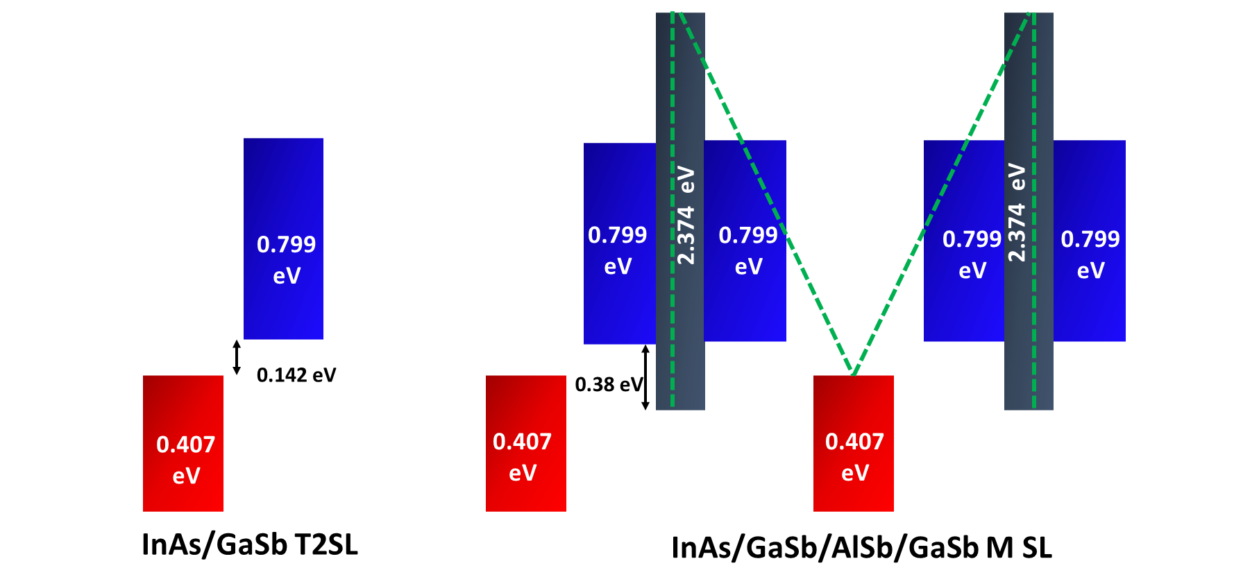
In these superlattices, as the additional potential due to the band, alignment is superimposed over the underlying atomic potentials, we implement the 8-band method with the envelope function approximation (EFA). To obtain the energies and their corresponding wavefunctions, the finite difference method (FDM) with periodic boundary conditions are employed to solve this HamiltonianGaleriu (2005); Mukherjee et al. (2021); Seyedein Ardebili et al. (2023). Additionally, we treat the interface as an InSb layer with 3Åwidth in one superlattice period to account for the lattice mismatch in these non-common atom configurationsSzmulowicz et al. (2006); Delmas et al. (2019). The interband momentum matrix parameter is calculated by the weighted average of InAs, GaSb, InSb, and AlSb layers. The parameters for InAs, GaSb, InSb, and AlSb materials are provided in Table 1. Figure. 1 shows the band alignment in T2SL and MSL. The following equations are implemented to calculate the density of states of these superlattices utilizing the 8-band method Benchtaber et al. (2020); Benaadad et al. (2021),
| (11) |
where, i is the index that represents the band, and are the energies at the , and , respectively, is the effective mass, and is the wavevector along the growth direction. The miniband width of the superlattice is defined by the term .
| Parameters | InAs | GaSb | AlSb | InSb |
| Valence band offset (VBO) [] | -0.56 | 0 | -0.38 | 0.03 |
| Lattice constant (Å) | 6.0522 | 6.0854 | 6.1297 | 6.4717 |
| Spin-orbit splitting (SO) [] | 0.38 | 0.75 | 0.65 | 0.81 |
| Optical matrix parameter ( Ep []) | 21.5 | 22.4 | 18.7 | 23.3 |
| Luttinger parameter () | 19.4 | 11.84 | 4.15 | 32.4 |
| Luttinger parameter () | 8.545 | 4.25 | 1.28 | 13.3 |
| Luttinger parameter () | 9.17 | 5.01 | 1.75 | 15.15 |
| Corrected Luttinger parameter () | 6.30 | 4.86 | 1.76 | 16.78 |
| Corrected Luttinger parameter () | 1.99 | 0.76 | 0.085 | 5.61 |
| Corrected Luttinger parameter () | 2.62 | 1.52 | 0.55 | 7.46 |
| Effective mass electron () | 0.022 | 0.0412 | 0.13 | 0.0135 |
| Corrected Effective mass electron () | 2.51 | 1.053 | 2.716 | 1.84 |
| Energy band gap at T=77K() | 0.407 | 0.799 | 2.374 | 0.227 |
II.2 Absorption coefficient and optical moment matrix element
The optical absorption coefficient represents the value that how far the light travels in the material before being absorbed. It gives an idea of how readily the light is absorbed in the material and contributes to the generation of electron-hole pairs, which will later contribute to the photocurrent in the device. It is a product of the joint densities of states and the Fermi function, which can be calculated by Fermi’s Golden Rule Qiao et al. (2012) and represented as
| (12) |
where n represents the refractive index of the superlattice, denotes the permittivity of the free space, , are conduction and valence band energies calculated by the 8 band theory at a particular , m and n are the valence and conduction band indexes, w is the incident photon frequency, and are the Fermi functions and , are the quasi-Fermi levels calculated at certain doping, and is the Lorentzian function, given by
| (13) |
where the parameter is used for the scattering processes, also called as broadening function and the value taken in this work is both for the T2SL and MSL. The Fermi functions are denoted as and and can be expressed as
| (14) |
| (15) |
where, is the Boltzmann constant, and other parameters are the same as in the functions discussed above.
Further, the term in equation 12, i.e., is the optical matrix moment elements which represents the transition probability from the filled valence band to the empty conduction band and is calculated by equations given in Qiao et al. (2012), which mainly depends on the overlap of the envelope wavefunction w.r.t to the space and the transverse wavevector. Both the TE and TM polarization matrix elements which are required for the calculation of the absorption coefficients are calculated by the equation as given in Qiao et al. (2012). Where, the absorption includes the upward transition, the opposite of absorption is spontaneous emission, which considers only the downward transition and requires the initial conduction band state to be occupied, and the final valence band state to be empty. The spontaneous emission rate is given by
| (16) |
where all the terms are similar to absorption but according to the occupancy of electrons and holes in conduction and valence bands, there is a difference in the terms representing the Fermi function.
II.3 Carrier lifetime
The generated electron-hole pairs in the active region should get transmitted to their respective contacts for the photocurrent. In addition, the diffusion length of the minority carriers are to be higher than the absorption length only then they can participate in the photoconduction, otherwise, they will just lost by the recombination process in the device. Therefore, the minority carrier’s lifetime is a crucial parameter, as it determines both the dark current and maximum operating temperature for the acceptable performance of the photodetectors. The diffusion-limited detector dark current Olson et al. (2015) in the n-type doped material is given by
| (17) |
where represents the electronic charge, is the intrinsic carrier density of the material, is the electron concentration which is in the majority, and is the thickness of the active region, and is the minority carrier lifetime. The lifetime of the carriers depends on the various recombination phenomena, which are Schockley-Read-Hall(SRH), radiative, and Auger recombination. The SRH recombination process is due to the defect levels present in the material, which restricts their flow as the carries get trapped in the trap level given by
| (18) |
where, , , the overall electron and hole concentration, is the excess carrier concentration(=) and the and can be expressed as
| (19) |
where is the intrinsic energy level, and the is the trap level, respectively. The SRH lifetime Höglund et al. (2013) depends on the electron and hole capture constants which are given by
| (20) |
where, are the capture cross-section area for the electron and hole defect, respectively, and is the thermal velocity of the carriers. For an n-type material and assuming the trap level at midgap, the SRH lifetime Olson et al. (2015) can be represented as
| (21) |
In case of low level injection, with the , can be denoted as and similarly for the p-type it will be .
The radiative recombination coefficient which involves the band-band transitioning from the conduction band to the valence band Trupke et al. (2003); Azarhoosh et al. (2016) is calculated by the following equation
| (22) |
where is the absorption coefficient at frequency w and temperature T, and is the refractive index of the superlattice material.
III Results and discussions
Electrons in the T2SL are delocalized, which leads to conduction via minibands, while hopping occurs for holes due to their higher localization in GaSb wells Klipstein et al. (2021); Singh et al. (2022); Hussain et al. (2022); Ting et al. (2011). These localization effects depend on the thickness of InAs and GaSb taken in one superlattice period. The carriers’ localization and wavefunction overlap play a significant role in determining the optical and dark current characteristics of T2SLNghiem et al. (2017); Imbert et al. (2015); Singh and Muralidharan (2022). For the design of barrier-based photodetectors (XBp), three regions in particular—contact(X), barrier(B), and absorber(p-type)—must be considered Nguyen et al. (2009). T2SL is applicable to design these regions due to the tunability of the conduction and valence band edgesAkhavan et al. (2016); Mukherjee and Muralidharan (2018); Delmas et al. (2019); Razeghi and Nguyen (2010). The valence and conduction band offsets between the barrier and absorber layers decide the flow of photogenerated carriers from the absorber to the contactsKopytko et al. (2015); Li et al. (2019). In this work, we examine the effect of carrier localization on the absorption and dark current properties of T2SL and MSL for the LWIR and MWIR applications. The same bandgap T2SL and MSL are also explored to study the effect of InAs, GaSb, and AlSb layer widths on quantum efficiency and minority carrier lifetime. We also showcase the design of the barrier to design the XBp detectors. The barrier blocked certain density-of-states which restricts the photogenerated carriers’ flow in one direction only.
III.1 Absorber
Reduced SRH, Auger, and radiative recombination dark currents that led to higher operating temperature can be achieved owing to the spatial confinement of carriers in the InAs/GaSb T2SL(holes in GaSb well and electrons in InAs well)Kopytko et al. (2015); Li et al. (2019); Downs and Vandervelde (2013). In this work, we want to design an absorber for the XBp barrier-based IR detectors, where most of the depletion region falls in the barrier(B) region, and due to its higher bandgap, the SRH dark current component reduces. The barrier further reduces the band-to-band dark tunneling currentsLi et al. (2019); Singh et al. (2022); Kopytko et al. (2015). To achieve higher quantum efficiency, we investigate a p-type doped absorption region almost at equilibrium (the depletion region shifts more toward the barrier region).
III.1.1 InAs/GaSb Type-II superlattice Absorber
To obtain the electronic band structure characteristics of T2SL, we apply an 8-band perturbative method as discussed in section II.A. We consider InSb as
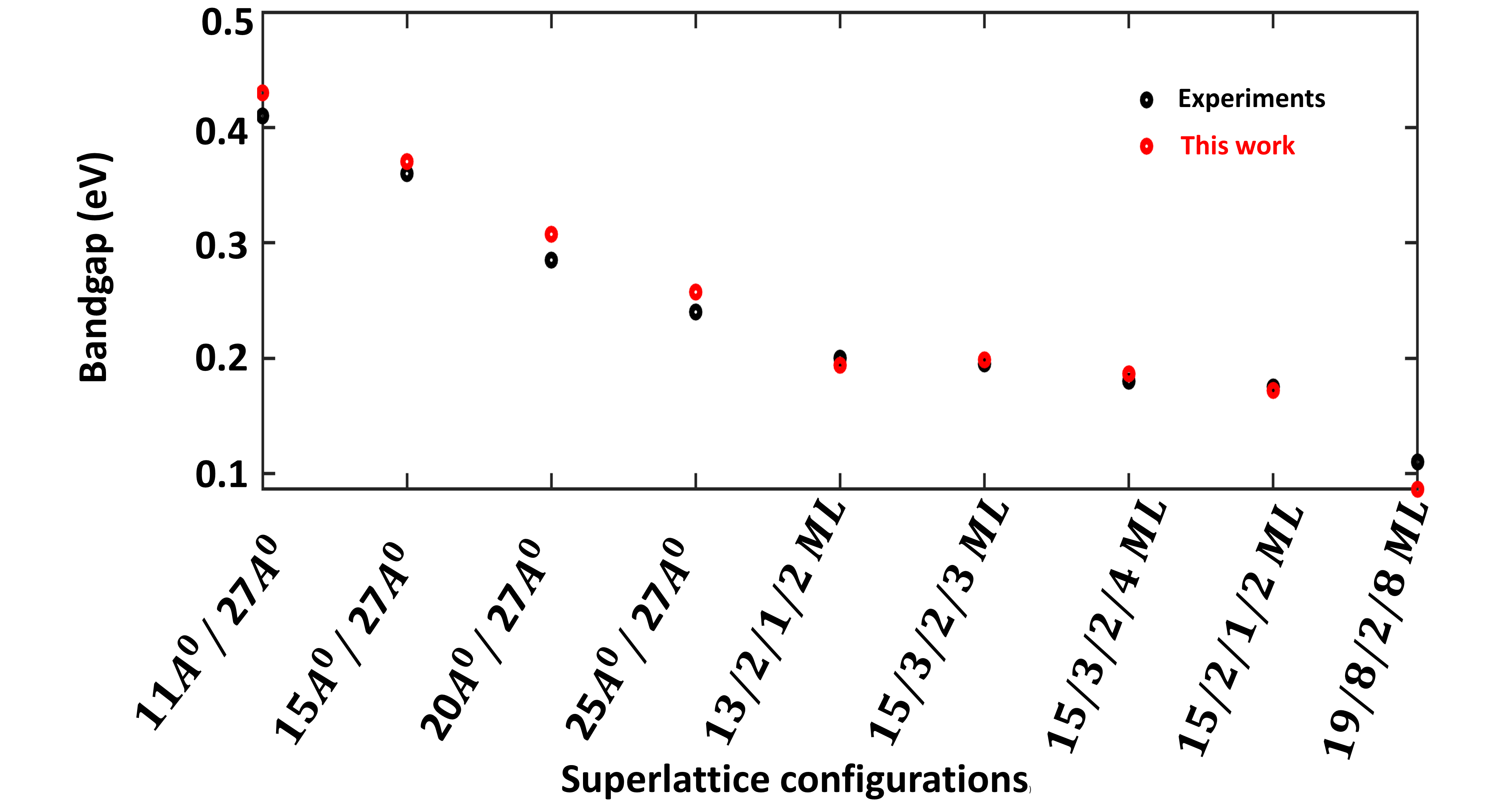
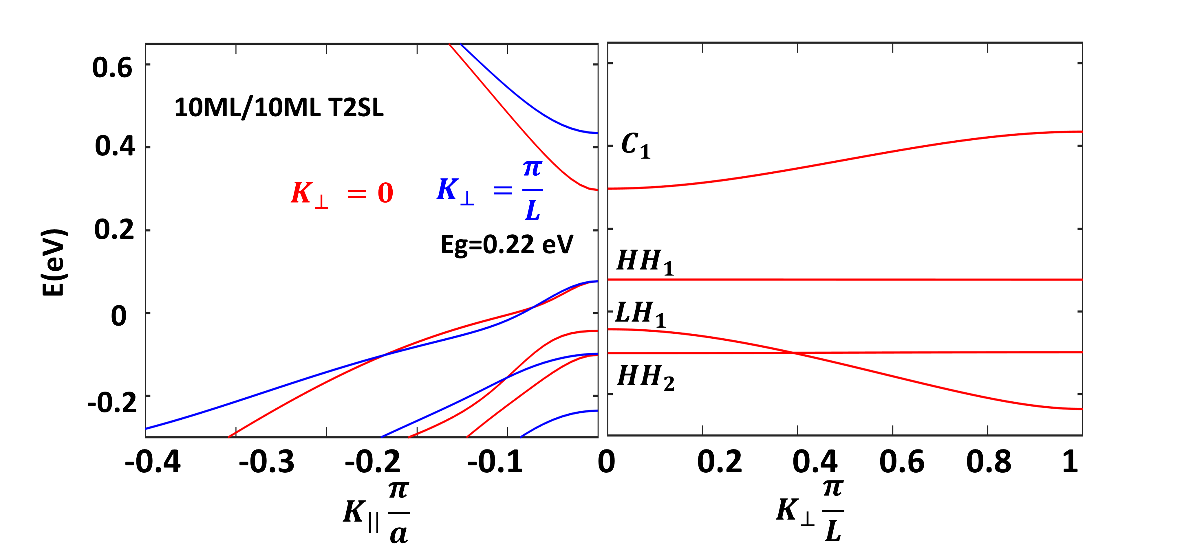
the interface, and the width is 3ÅQiao et al. (2012); Delmas et al. (2019). We plot our simulated results with existing experimental or simulation values from the literature in Fig. 2 to validate our results. We then calculate the band structure of 10ML/10ML T2SL, as shown in Fig.3, where we see an almost dispersion-less E-k plot in the growth direction for holes because they are highly localized in the GaSb quantum well. While the electrons are delocalized, this can be seen from both the energy dispersion and the conduction band mini-bandwidth (difference between red (=0) and blue (), the mini-bandwidth of the holes are a few , while an electron’s miniband width is around .
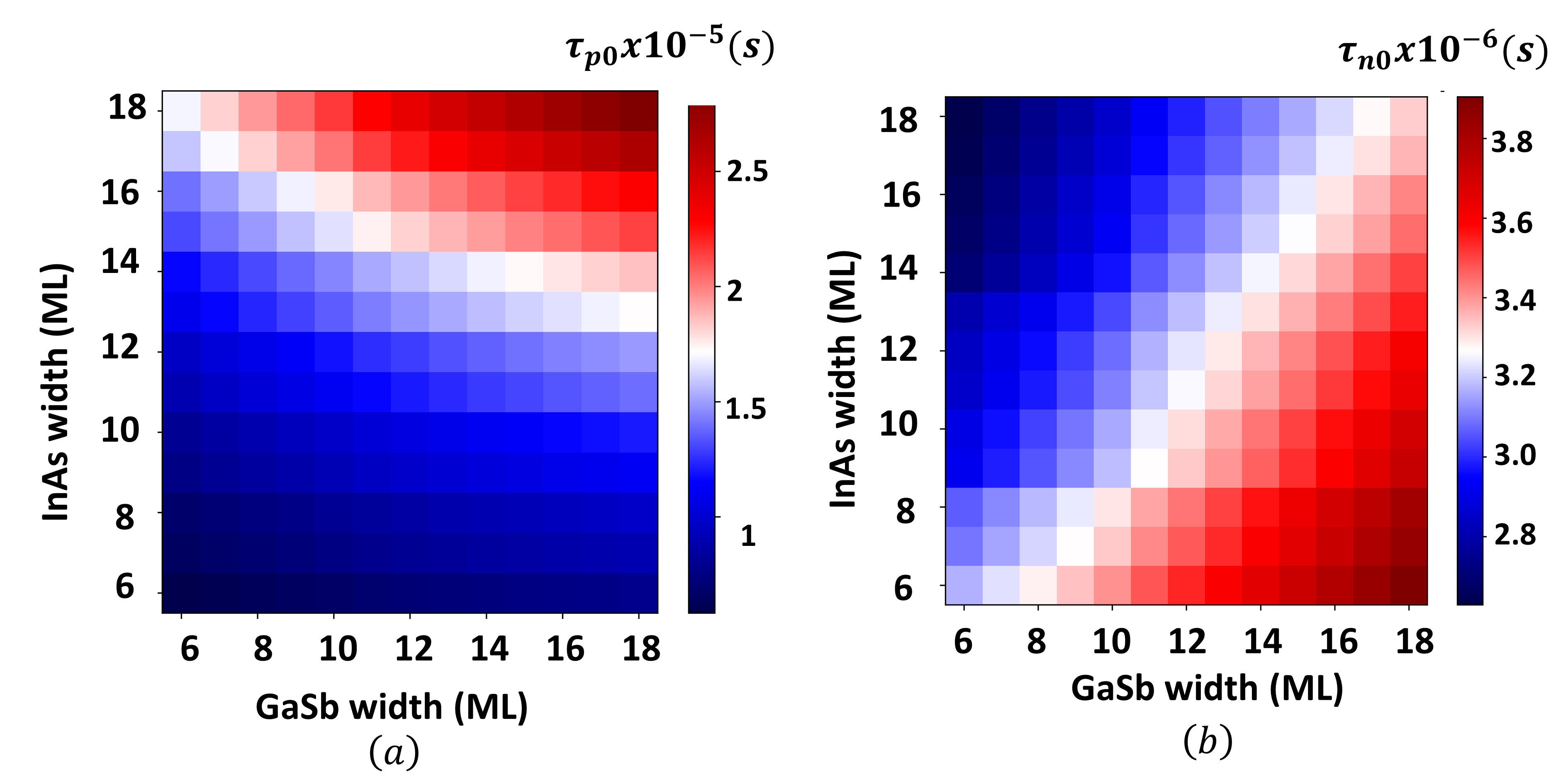
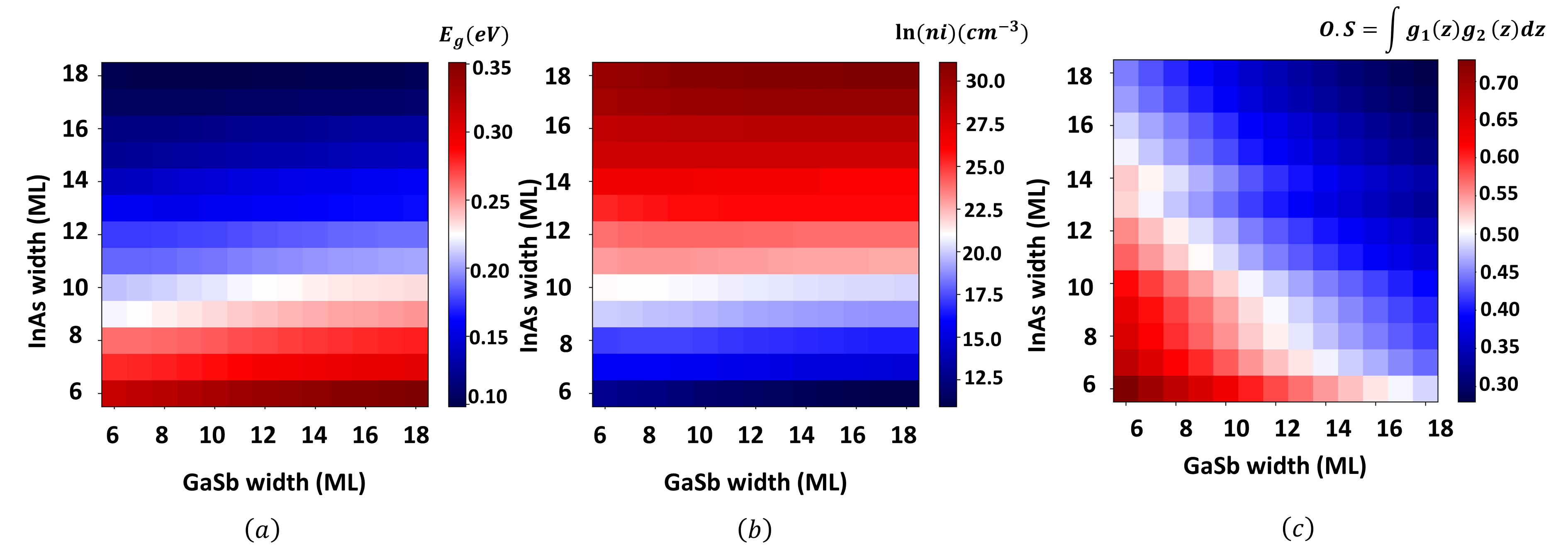
Next, we calculate the bandgap, intrinsic carrier concentration (), oscillator strength (O.S), SRH, and radiative recombination coefficients for different T2SL compositions while varying the thickness of both InAs and GaSb from 6 ML to 18 ML. The bandgap () 2D color plot is plotted in Fig. 4 (a), and we notice that the bandgap decreases with increasing InAs width (at constant GaSb width) and changes proportionally with GaSb width (at a constant InAs width). Figure. 4 (b) shows the variation of with the InAs and GaSb widths. A rapid rise in is seen with the increment in the InAs width as the reduces and the effective masses of the holes increaseMukherjee et al. (2021); Singh et al. (2022); Delmas et al. (2019).
For a constant InAs width while increasing the GaSb width, decreases as increases (conduction band split reduces, shifts upwards), but the change is not very significantSingh et al. (2022).
In Fig.4 (c), we calculate the oscillator strength (O.S) of the first conduction and heavy hole (-) transition at the Brillouin zone center by using , which is the product of the dominant envelope wavefunction for the conduction () and heavy hole band (). The O.S decreases with the increased width of the InAs and GaSb as the confinement of the carriers in their respective wells increases; therefore, the thicker superlattices have less absorption than the thinner ones. Figures. 5 (a) and (b) show the SRH recombination capture time constants necessary to compute the SRH lifetime, and , as a function of the thermal velocities of the carriers, which in turn relies on the effective masses ()Aytac et al. (2016); Klein (2014); Aytac et al. (2015). The capture time constants ( and ) are calculated by equation 20. We consider a trap energy level of 45 above the valence band edge and a cross-sectional area of and to calculate the SRH lifetime constantsConnelly et al. (2010). From Fig. 5 (a), we notice the increment in the hole capture lifetime () as the InAs width is increased while keeping the GaSb constant. Here, the effective mass of the hole increases with the higher InAs width, causing the thermal velocity of holes to drop and hence the (inversely proportional to thermal velocity) to increase. The electron capture time constant () increases with increasing GaSb width for any constant InAs width, because the electrons become more confined in the InAs well, which leads to higher effective mass and thus a lower thermal velocity, as shown in Fig.5 (b).
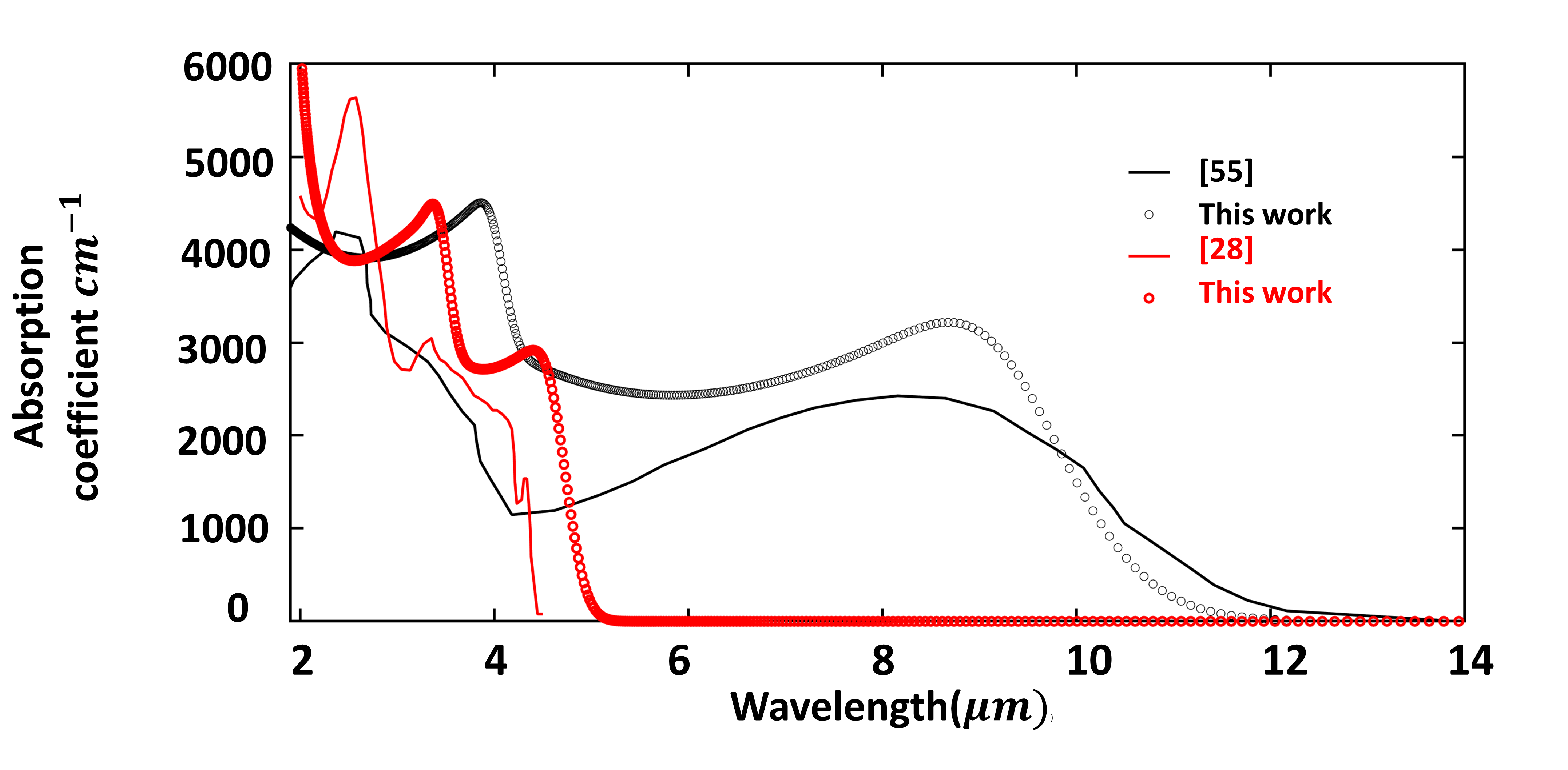
After investigating the SRH recombination carrier lifetimes, which dominate at lower temperatures, we now apply Fermi’s golden rule to calculate the absorption coefficient. The required optical matrix moment elements are calculated by the 8-band theory as described in section II.B. We confirm our simulated absorption coefficients with experimental values as shown in Fig. 6, where the
absorption coefficients for the 8.5ML/13.6ML and 15ML/7ML T2SL wavelengths, which are approximately and cut-off wavelength, respectively, are calculated at T=77K. The results are consistent with the experimentally demonstrated value.
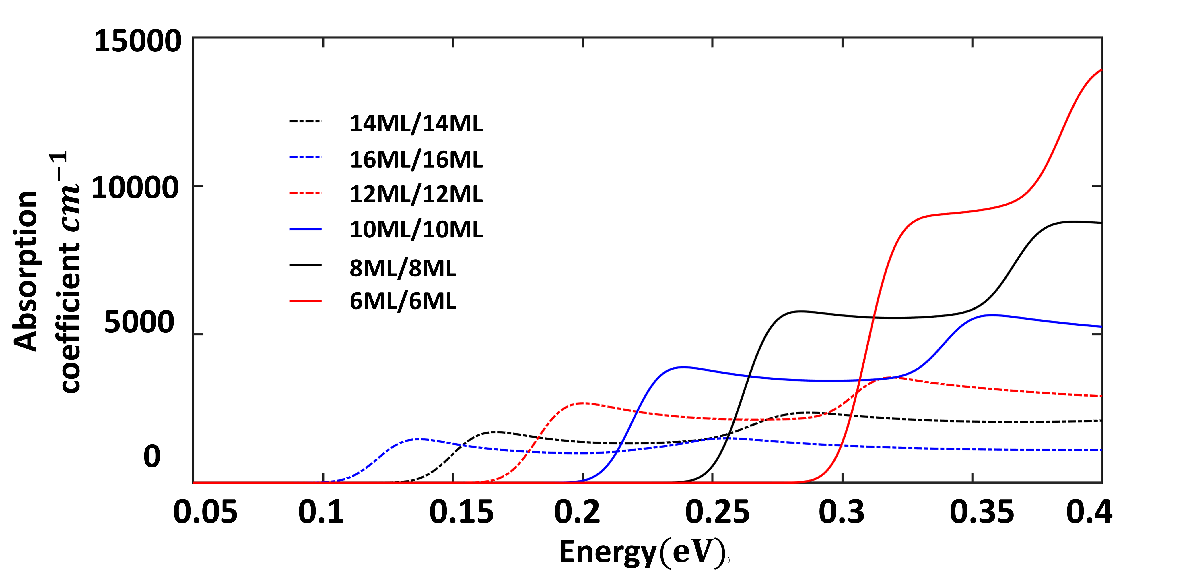
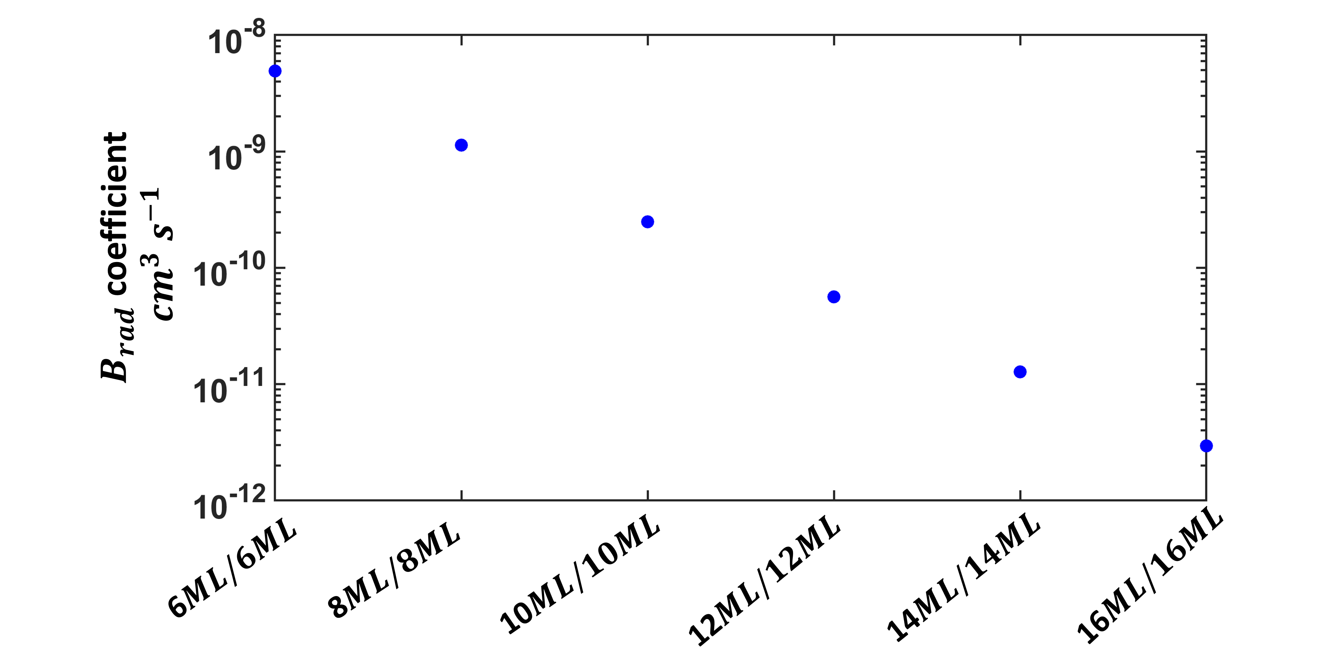
After validating our absorption model, we calculate the absorption coefficients for the 6M/6ML, 8ML/8ML, 10ML/10ML, 12ML/12ML, 14ML/14ML, and 16ML/16ML T2SL with a doping concentration of (p-type doped) to study the variations in the optical properties of T2SL with respect to the InAs and GaSb compositions.
The p-type doping is taken into account in the absorber because the minority carriers, which are electrons in p-type, have a longer diffusion length; therefore, they contribute more to photocurrent, and thus a higher quantum efficiency can be achieved. By increasing the widths of InAs and GaSb from 6ML/6ML to 16ML/16ML, we observe a decrease in cut-off energy, as shown in Fig.7 (a). Also by increasing the width of InAs and GaSb, the confinement increases, due to which the carrier overlap at the interface decreases, which reduces the probability of their transition from a filled valence band to an empty conduction band and we notice lower absorption coefficient values in Fig.7 (a).
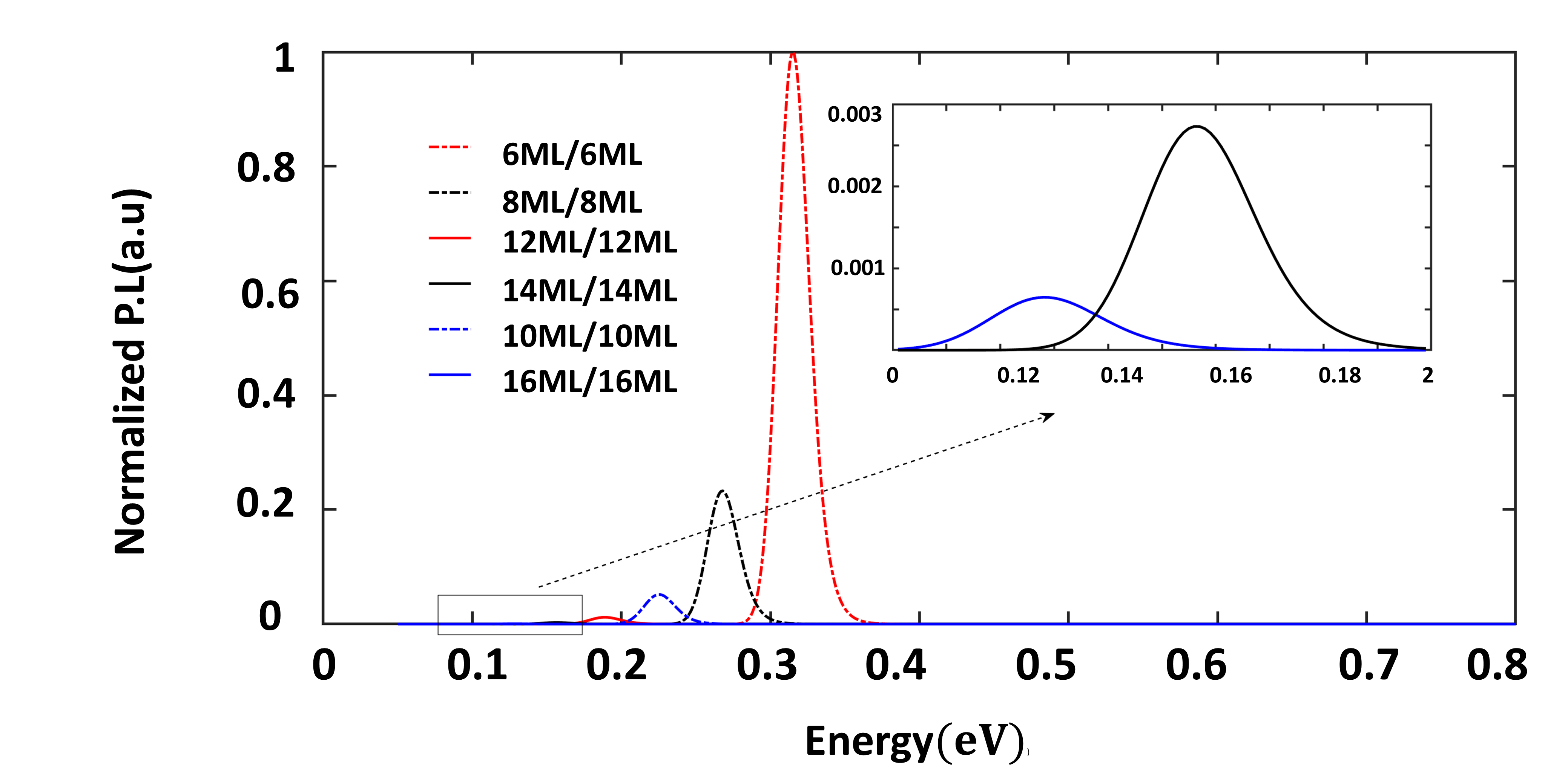
Since the photoluminescence (PL) spectra correspond to the spontaneous emission rate at lower doping, we then calculate the PL spectra of T2SL at low injection levels, where we keep the excess carrier concentration as , and the acceptor’s concentration () is and plot the PL spectra in Fig.7 (b). We see a red shift in bandgap while increasing the widths from 6ML/6ML to 16ML/16ML for these T2SLs as shown in Fig.7(b).
The intensity of the PL peak decreases as the width of InAs and GaSb increase, which is because the downward transition, i.e., from the filled conduction band to the empty valence band, is smaller when the joint density of states (responsible for absorption also) is less as the spatial overlap of the carriers is less due to higher localization in their respective wells, and therefore, the PL intensity reduces. The PL intensity and absorption are also dependent on the quasi-Fermi levels, the PL intensity increases with acceptor doping, and the absorption decreases with acceptor doping. The values of and as taken in equation 11 are calculated by assuming the low injection by equations 14 and 15.
Furthermore, using equation 22, we estimate the radiative recombination coefficients () for these configurations and find that decreases as the widths of InAs and GaSb increase. As lowers, the carrier’s lifetime increases; hence, the 16ML/16ML has the longest radiative recombination lifetime.
III.1.2 InAs/GaSb/AlSb/GaSb M superlattice absorber
Since the addition of high-gap AlSb at the GaSb center in the InAs/GaSb/AlSb/GaSb MSL shifts the center of hole wavefunction near the InAs/GaSb interface and thus increases the absorption Lang and Xia (2013). We want to study the MSL to gain insight into this fact.
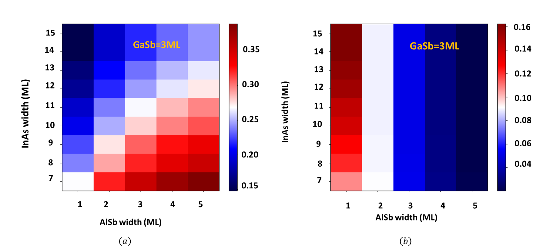
The electronic band properties of MSL, likewise the effective masses, the conduction and valence band edge tunability (with the InAs, GaSb, and AlSb), and density-of-states, we have reported in our previous work Singh et al. (2022). Here, we take a constant thickness of 3 ML of GaSb and change the InAs and AlSb widths from 6 ML to 15 ML and 1 ML to 5 ML, respectively, to see the effect of the AlSb width on the bandgap and the split-off energy (). From Fig. 9 (a), we deduce that the increases with the increasing width of AlSb because AlSb acts as an additional barrier to the electrons in the consecutive InAs wells, which further reduces the conduction band split and thus leads to an increase in . We also notice that the split-off energy decreases as the width of AlSb increases, as shown in the Fig. 9 (b), which plays a crucial role in hole-dominant Auger recombination (AM-7) currents.
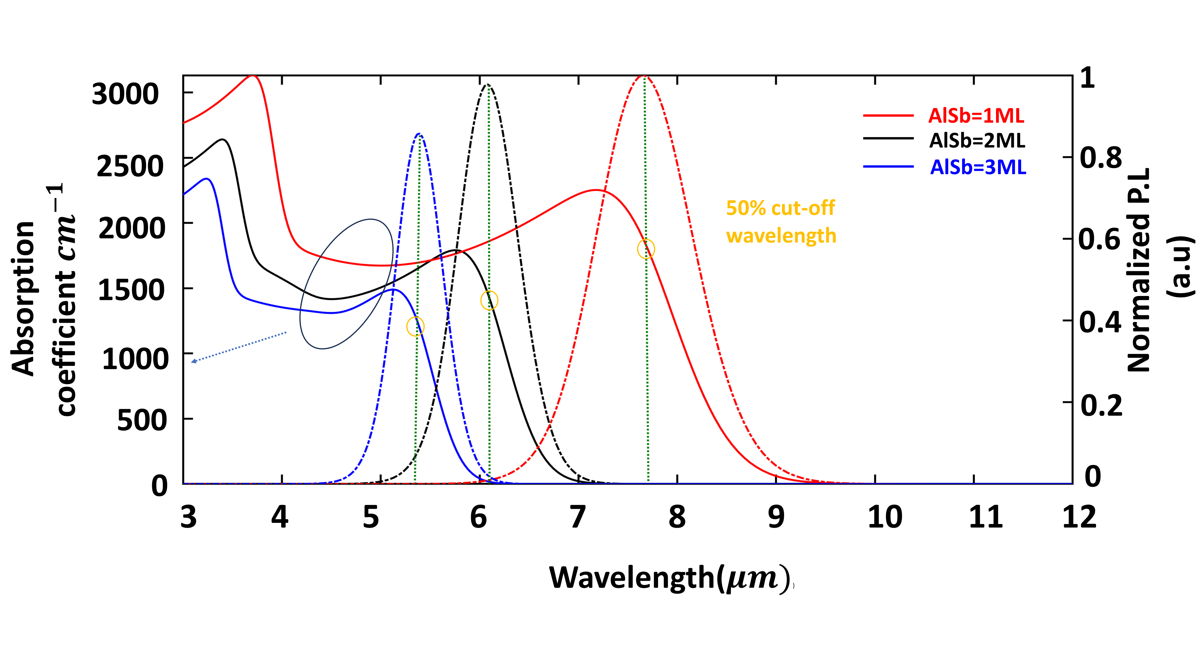
Next, in Fig. 10, the absorption and PL spectra are plotted for the 15ML/3ML/xML/3ML MSL, where the x varies from 1ML to 3ML, to notice the effect of AlSb width. The absorption coefficient values at the 50 % cut-off wavelength decrease. Also, the reduction in the 50% cut-off wavelength with the increase in the AlSb is seen in addition to the reduced PL intensity. It is noticed that the Full-width half maxima (FWHM) decreases with the increase in the AlSb width. The higher FWHM denotes the higher scattering and, hence, less carrier lifetime. Here, with the increase in the AlSb width, as carriers’ effective masses increaseSingh et al. (2022), they are less scattered in the material; therefore, there is a reduction in the FWHM with the increase in the AlSb width. The radiative recombination rate varies from to while increasing the AlSb width from 1 ML to 3 ML.
Since we can achieve the same bandgap with different compositions of T2SL and MSL compositions, we want to investigate the effect of InAs, GaSb, and added AlSb (in the case of MSL) on the optical and dark current properties of T2SL and MSL. Therefore, in the following sections, we compare the two same bandgap T2SL and MSL absorbers for the MWIR and LWIR infrared photodetection.
| Parameters | T2SL | MSL |
| Bandgap (eV) | 0.1256 | 0.1255 |
| HH-LH splitting () | 0.1818 | 0.1262 |
| Electron effective mass | 0.0229 | 0.0293 |
| Hole effective mass | 0.6559 | 1.5065 |
| Intrinsic carrier concentration | ||
| Overlap integral value at K=0 (C1-HH1) | 0.4441 | 0.335 |
| Radiative recombination coefficient () | ||
| SRH |
III.1.3 Comparison for LWIR Absorber
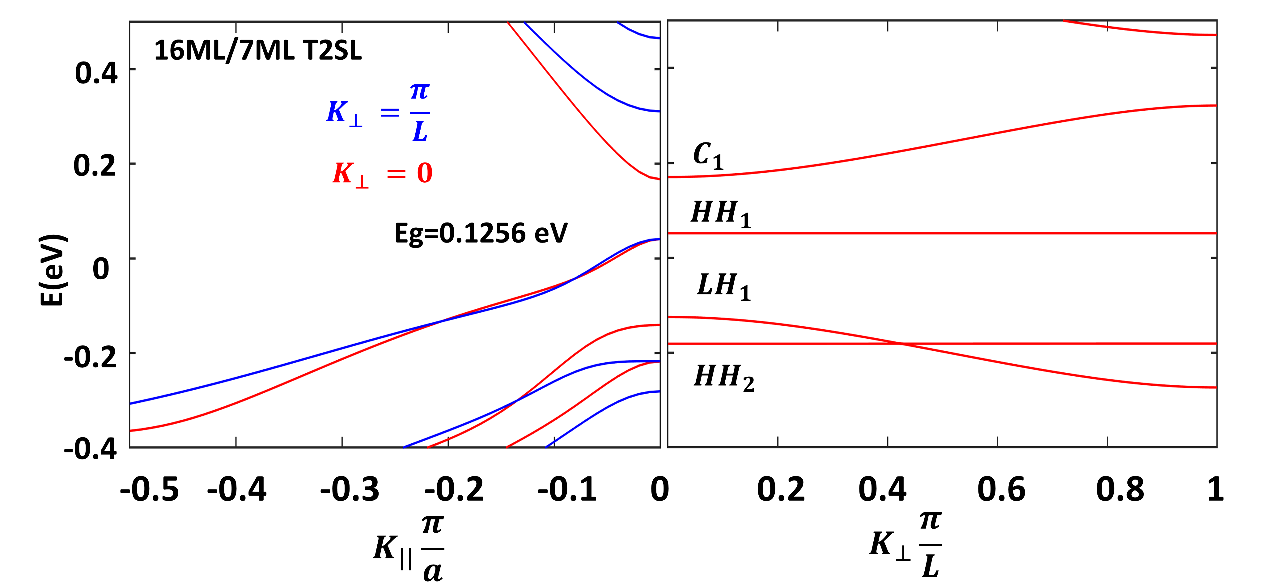
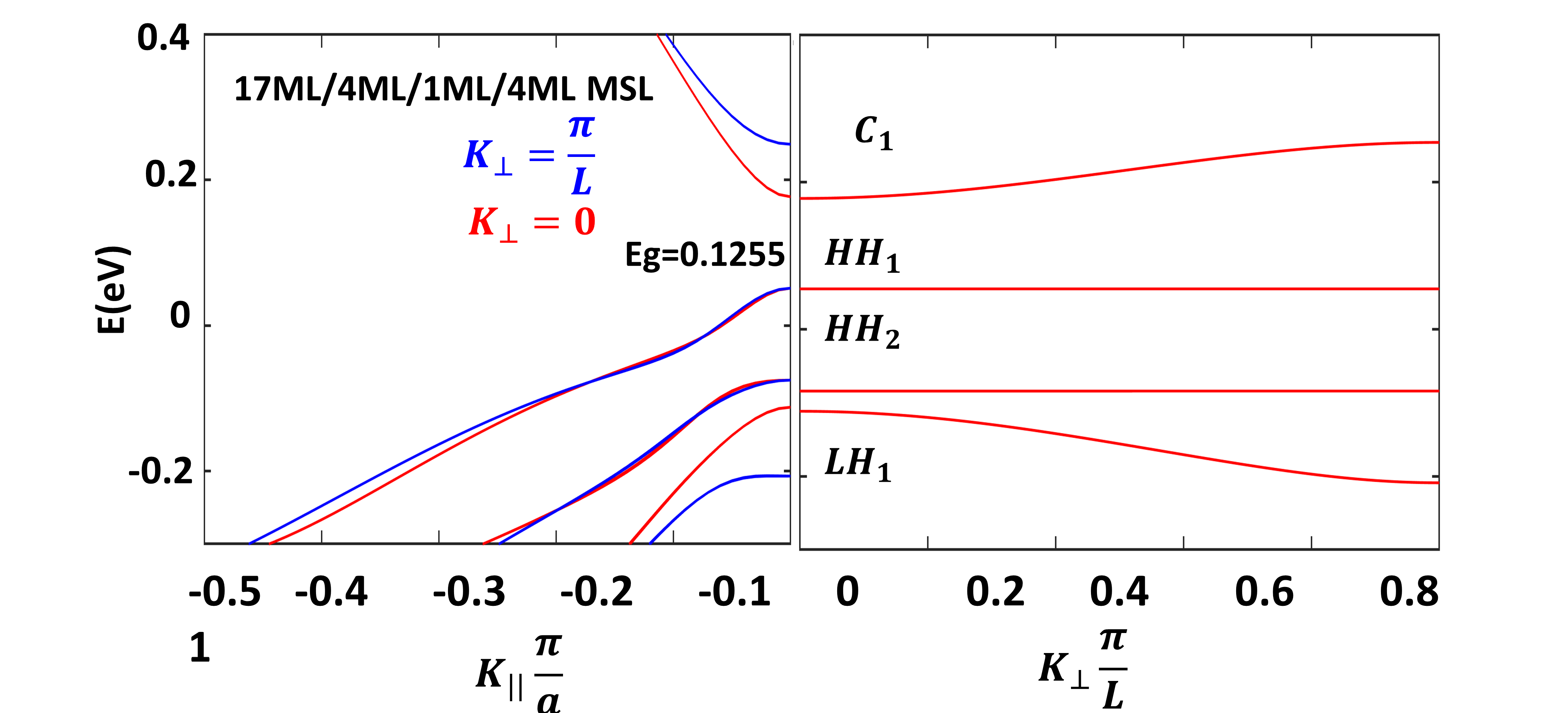
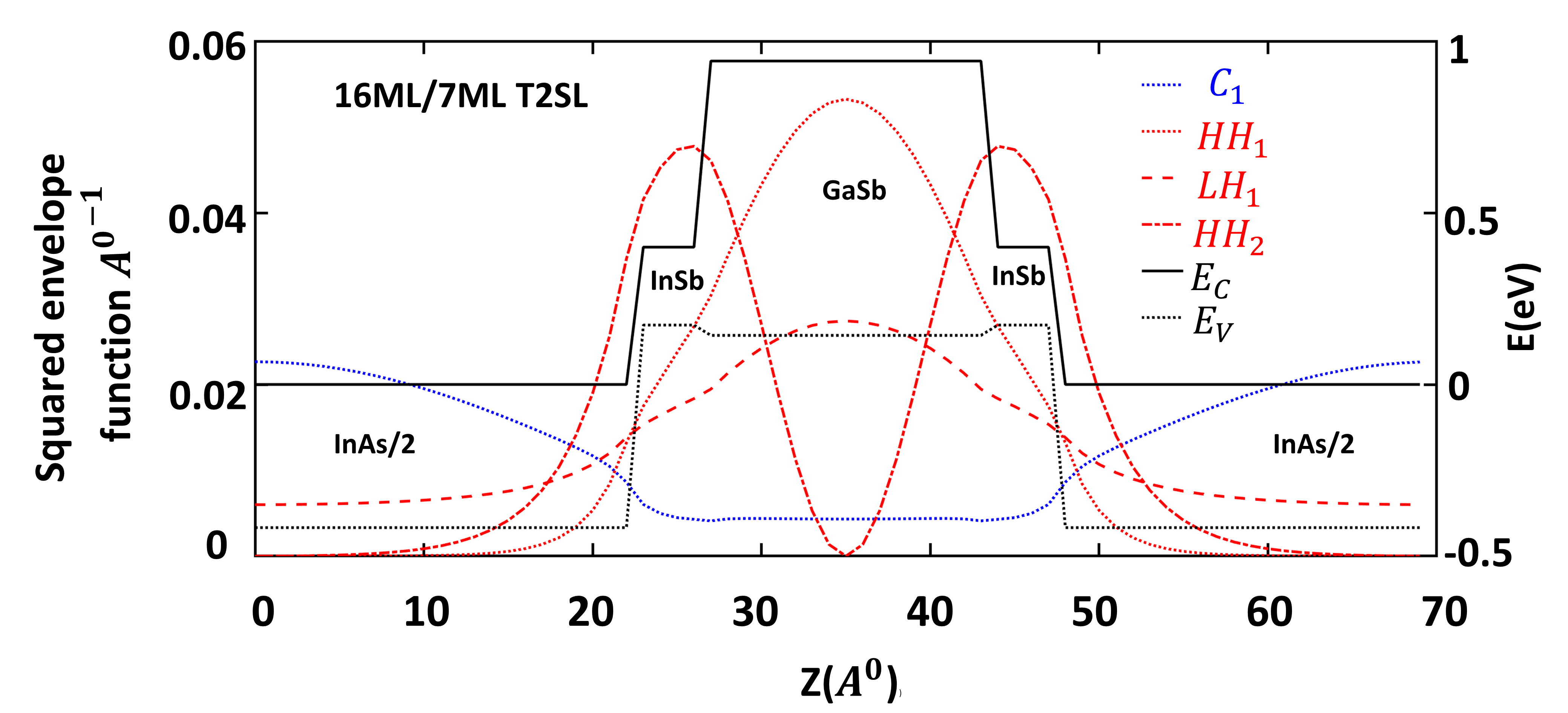
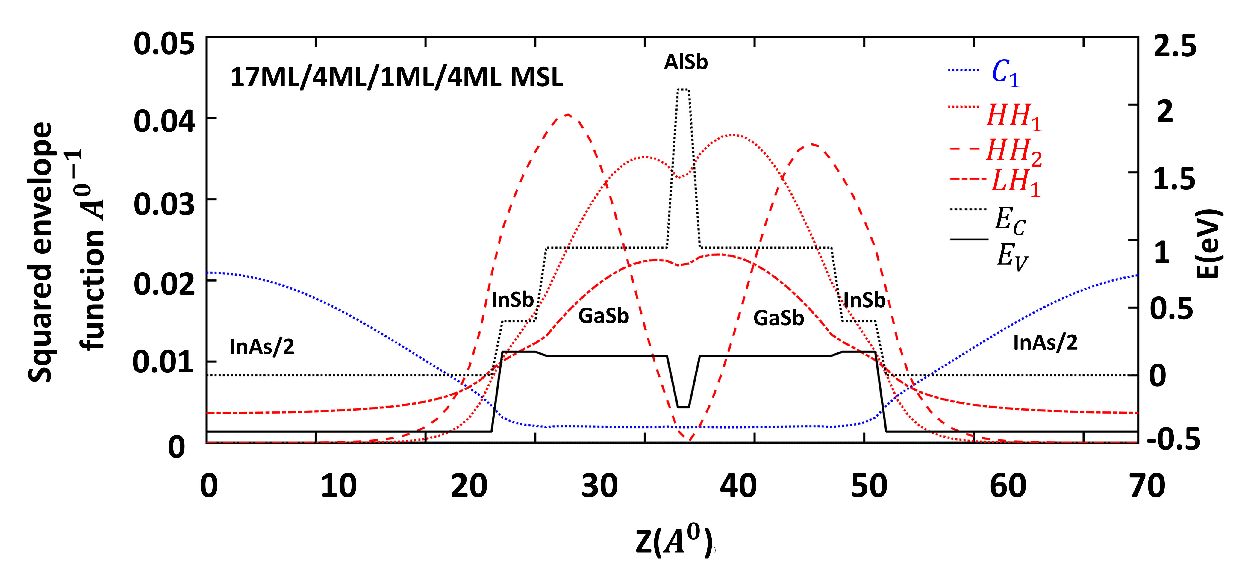
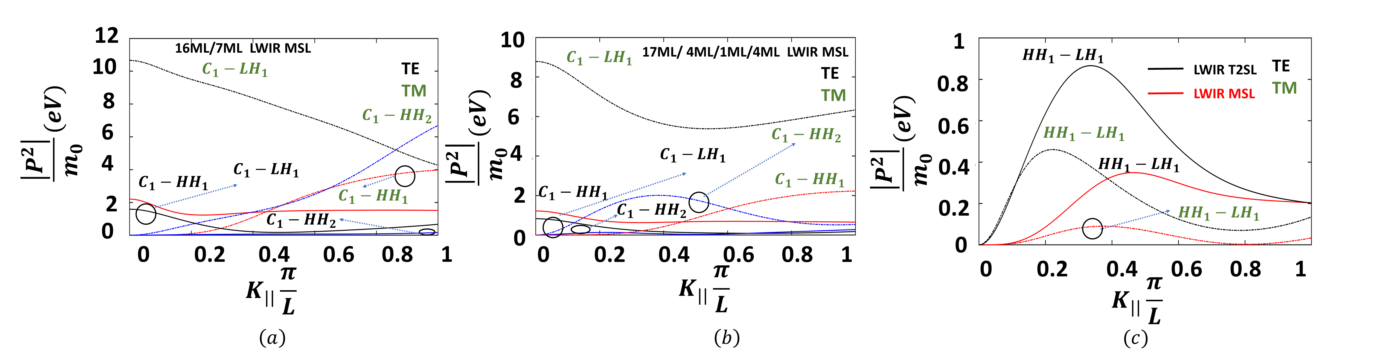
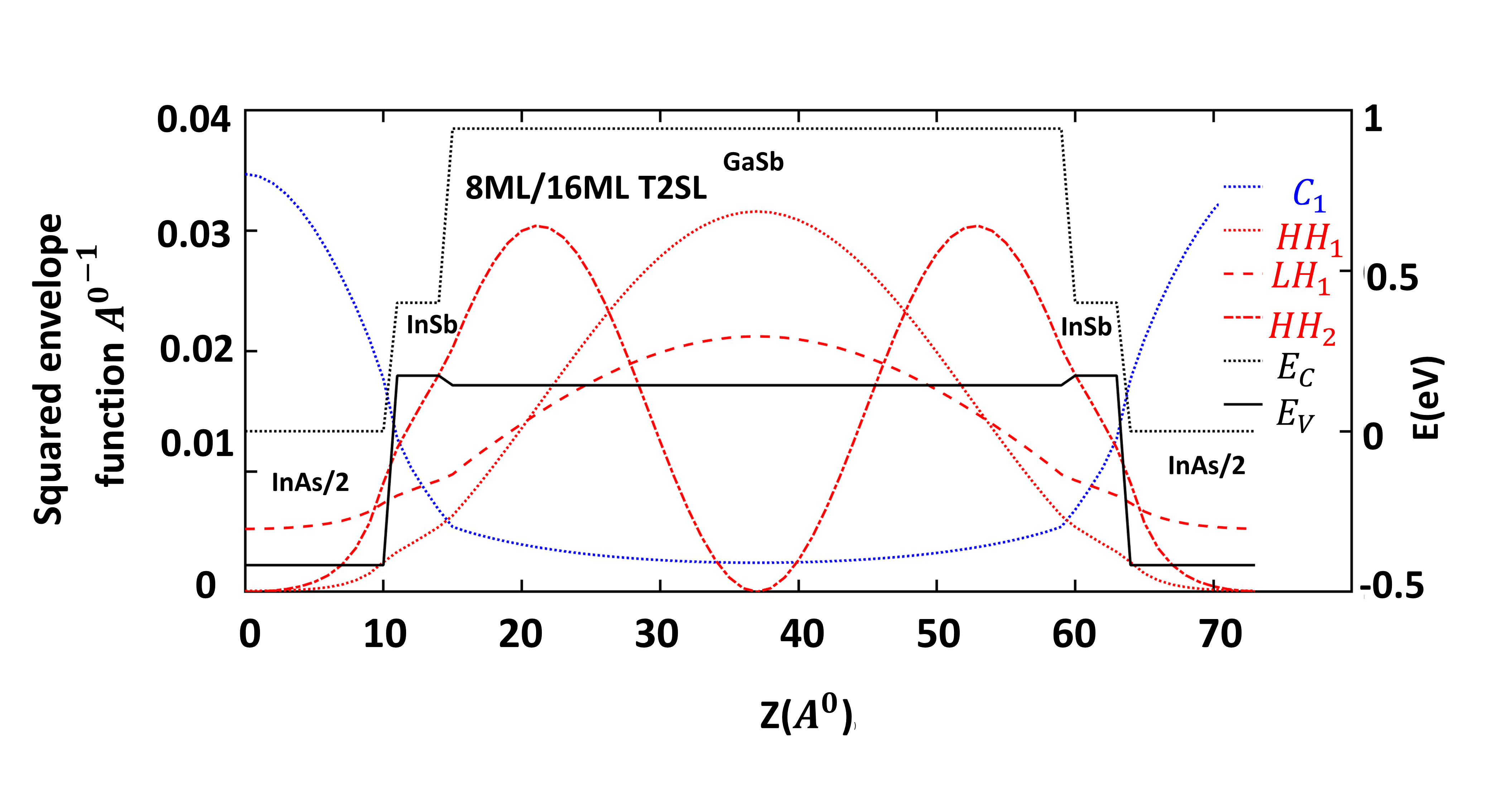
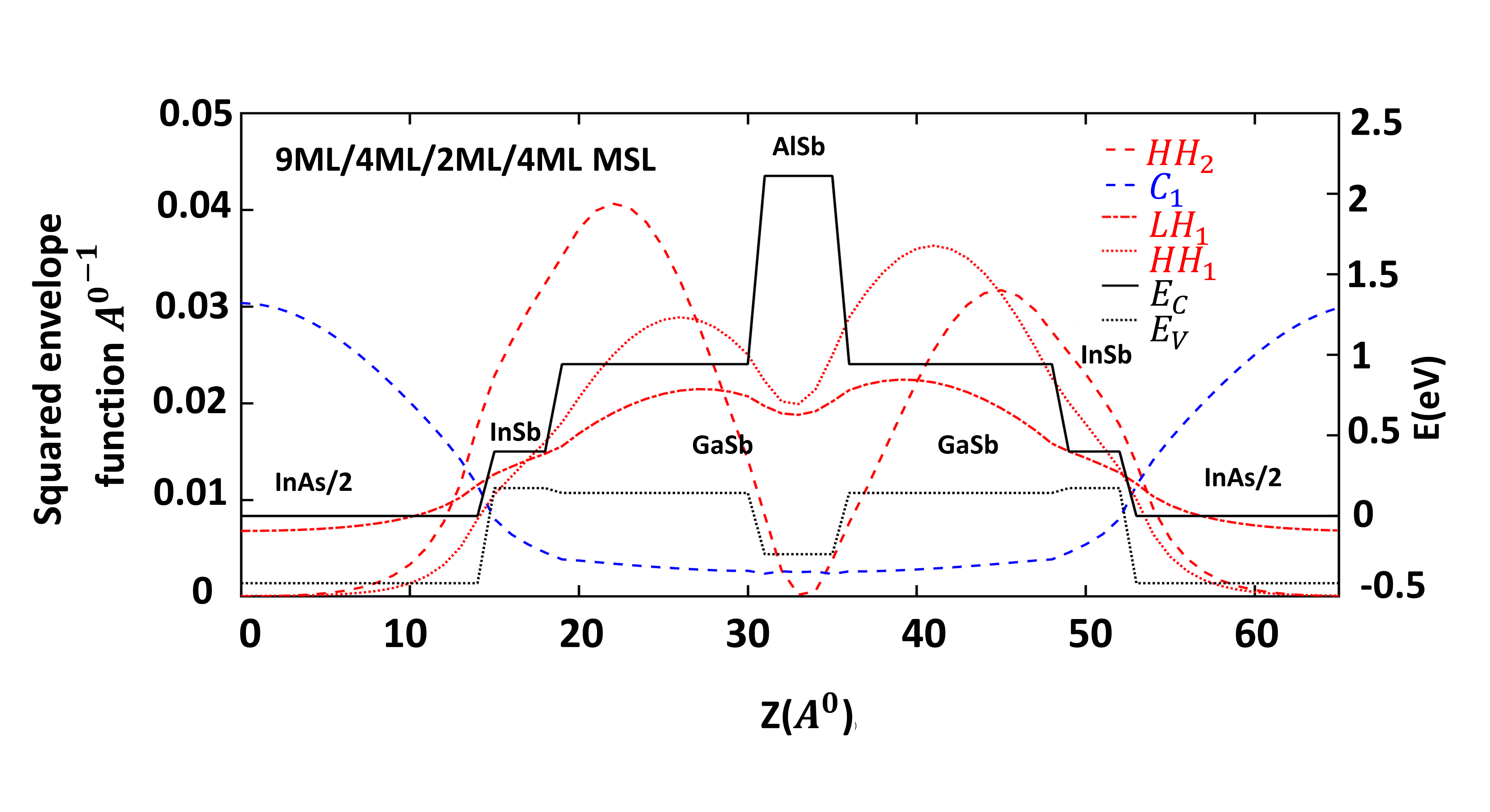
To examine the MSL as an absorber for LWIR applications, we design 17ML/4ML/1ML/4ML MSL and 16ML/7ML T2SL, which have the same bandgap of around 0.125. The band structures of 17ML/4ML/1ML/4ML MSL and 16ML/7ML T2SL are shown in Fig.11 (a) and (b), both in-plane and out-of-plane directions. For T2SL and MSL, the observed miniband width is approximately 142 and 72, respectively. To capture the overlap of the electron and hole wavefunctions at the interface, we consider the InAs/GaSb structure as (InAs/2)/GaSb/(InAs/2); thus 16ML/7ML is taken as 8ML/7ML/8ML. Similarly, the 17ML/4ML/1ML/4ML MSL is taken as 8.5ML/4ML/1ML/4ML/8.5ML. We plot the envelope wave functions corresponding to the first electron, the first heavy hole, the first light hole, and the second heavy hole at the Brillouin zone center () in Fig .12(a) and (b). These envelope wave functions are calculated from the Hamiltonian as discussed in section II.A. The
carrier type’s assignment depends on the envelope functions’ associated characteristics at Li et al. (2010). From Fig.12(a) and (b), it can be seen that the hole has a higher probability amplitude in the GaSb well, while the electron has more in the InAs electron well.
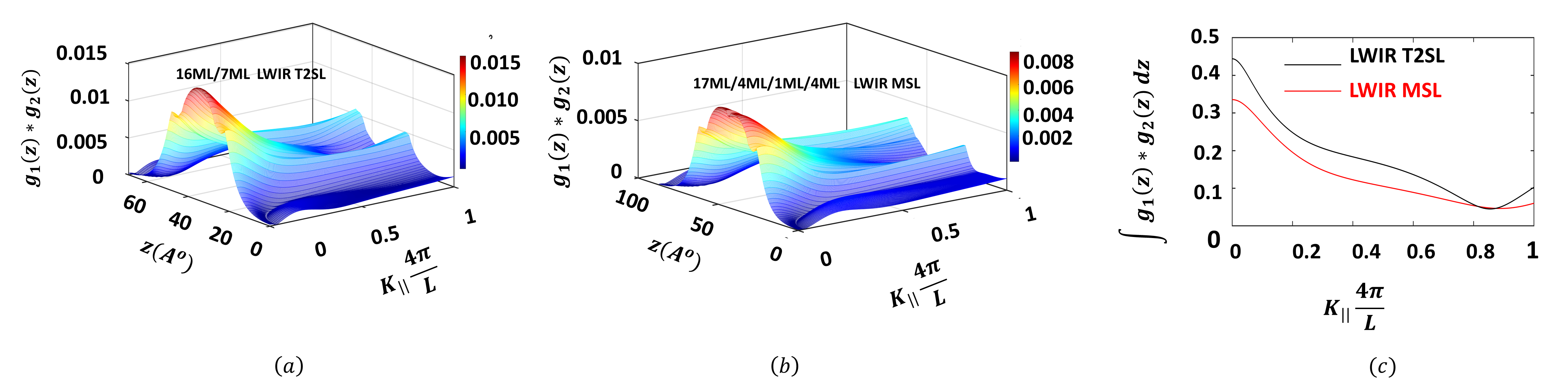
Also, in MSL, the AlSb has separated the GaSb hole quantum well into two newly generated wells for holes. The hole envelope wavefunction is shifted towards the InAs/GaSb interfaceLang and Xia (2013), as shown in Fig.12 (b). The heavy-hole probability is higher than the conduction band in both superlattices. Moreover, the light-hole occupation is less probable within the GaSb well, and subsequently, its leakage into the InAs barrier is higher than the heavy hole. Each wavefunction consists of eight envelope wavefunction components, which include one conduction and three valence bands plus their spins Galeriu (2005). These components are denoted by for the upper Hamiltonian, and corresponds to the lower Hamiltonian Ahmed (2016). The and are the notation for the conduction and valence bands, respectively. Now, we plot the spatial product, i.e., , in Fig. 13 (a) and (b). The and are the strongest components Ahmed (2016) of the envelope wavefunction of the first conduction () and heavy hole (). Here, we observe a higher spatial overlap near the InAs/GaSb interfaces in T2SL than in the MSL. This spatial overlap decreases as it moves away from the zone center ( ).
Next, the oscillator strength is calculated as , depict the transition probability from the to the Ahmed (2016).
In Fig.13 (c), we notice a higher oscillator strength for T2SL than in MSL.
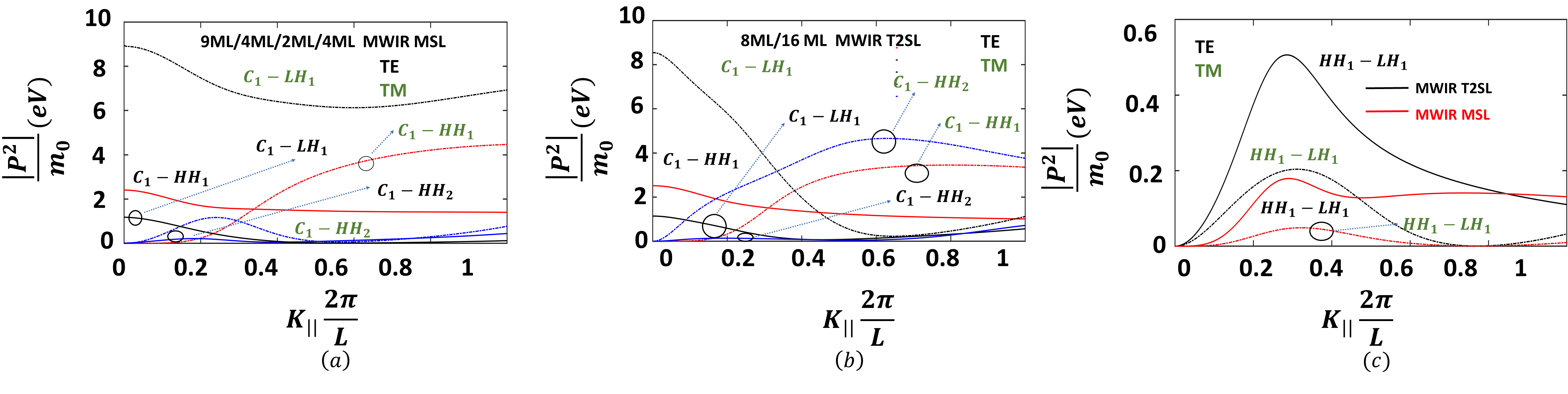
Further, we calculate the TE and TM momentum matrix elements to understand the allowed transitions from the first three valence bands to the first conduction band. We plot the TE and TM matrix elements as shown in Figs.14 (a) and (b). The dominant TE transitions are due to the - and -, whereas, - has been found to be less in the TE modeAndreev and Subashiev (2002). It can be observed that - is the strongest transition in the TM instead of -.
The TE component decreases in the C1-HH1 and C1-HH2 transitions, and the TM component increases from to Wang et al. (2016). Also, the calculated TM - transitions are larger than TE transitions for both T2SL and MSL. The - contributes the least to the absorption spectra even if it has a non-zero moment element, as their occupation probability is lower due to their separation from the fermi levels Wang et al. (2016).
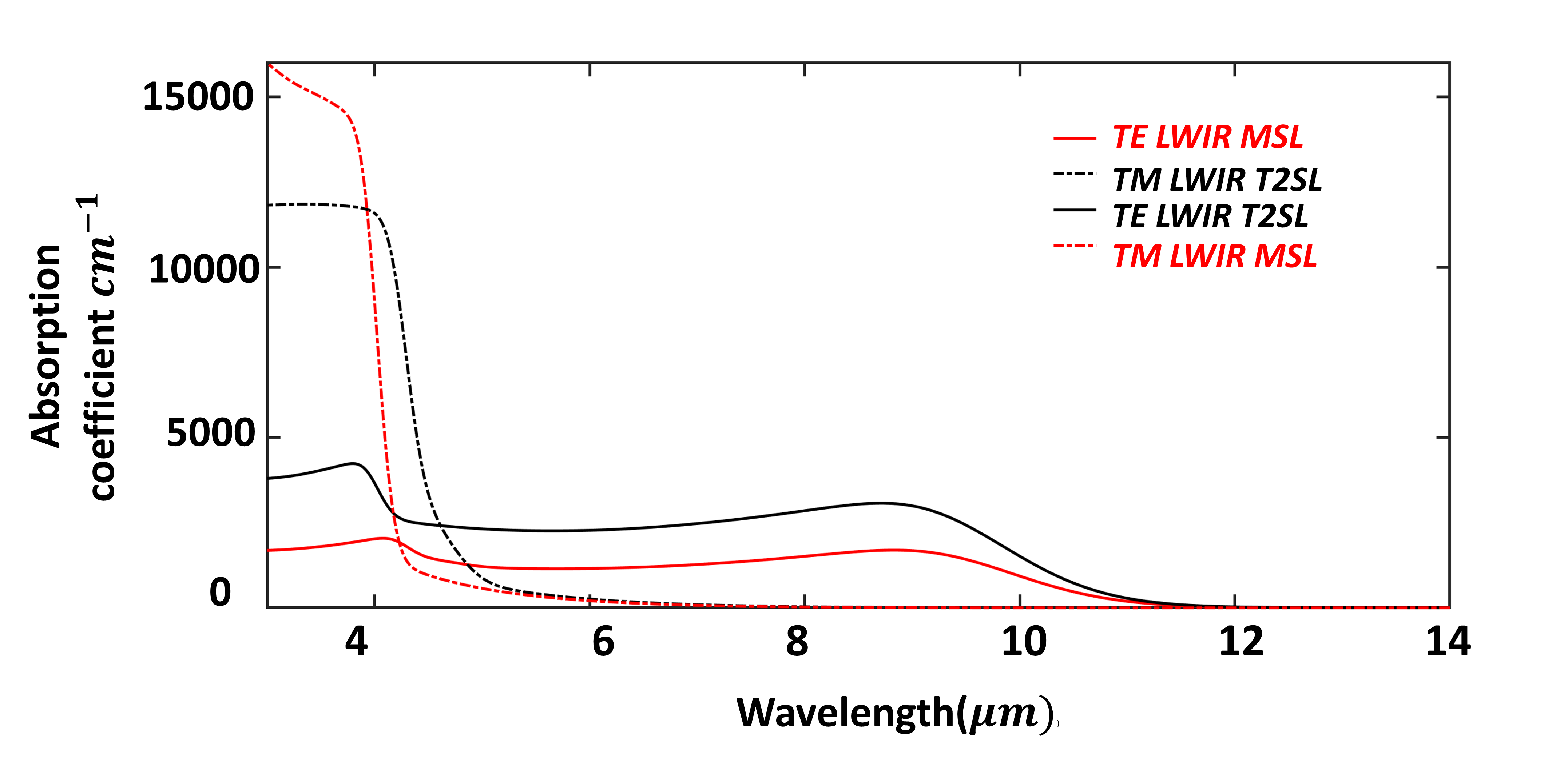
In Fig. 15 (a), we calculate the absorption coefficients for both the T2SL and MSL and notice that the T2SL has a higher absorption, which is related to its higher interface overlap and oscillator strength, as discussed above. Further, it has been noticed that after a specific excitation energy, the TM absorption increases and dominates the TEWang et al. (2016); Andreev and Subashiev (2002); Subashiev et al. (2004). This is explainable by the fact that the electron-transitioning from the with the angular momentum J=3/2, provides the filling of one electronic spin state in the conduction bandWang et al. (2016); Andreev and Subashiev (2002); Subashiev et al. (2004). Whereas, with the increase in the excitation the transitioning from the light-hole (J=1/2) also starts contributing to the absorption and filling of the second spin state in the conduction bandSubashiev et al. (2004).
Next, in Fig. 11, there is an - band mixing, after a certain while there is - band mixing even at for the MSL, this is due to the higher coupling of these bands due to InSb interfaceMagri and Zunger (2000).
To investigate the AM-7 (hole-hole dominating) Auger recombination, we plot the - transition probabilities for these SLs in Fig .14 (c) and observe a lower transition probabilities in MSL, resulting in a lower AM-7 auger recombination.
It can be seen that at lower values if the split-off is roughly equivalent to a bandgap, these probabilities increase, and later, they decrease. Also, the TE - is dominant over the TM - transition.
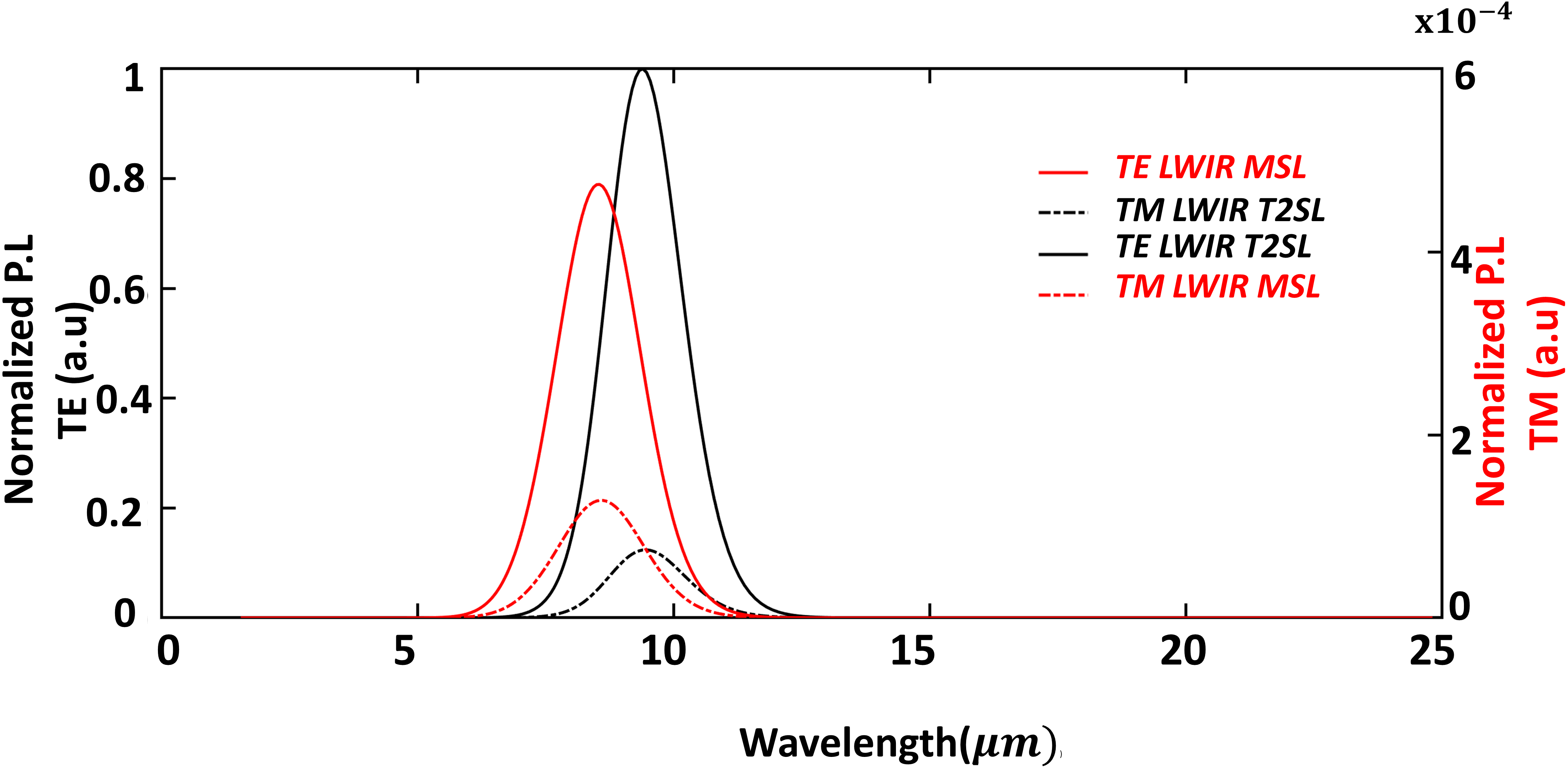
For both TE and TM modes, we calculate the spontaneous emission and plot the PL intensity in Fig.15 (b), and observe that the TM PL peak intensity is almost negligible in comparison to the TE PL peak intensity. We also, notice that spontaneous emission in MSL is lesser than in T2SL, which results in a smaller radiative recombination rate as shown in Table.2, and a longer lifetime in MSL, resulting in a lower dark current as well as improved quantum efficiency. Also, a shift in the PL peak is noticed in the TM polarization.
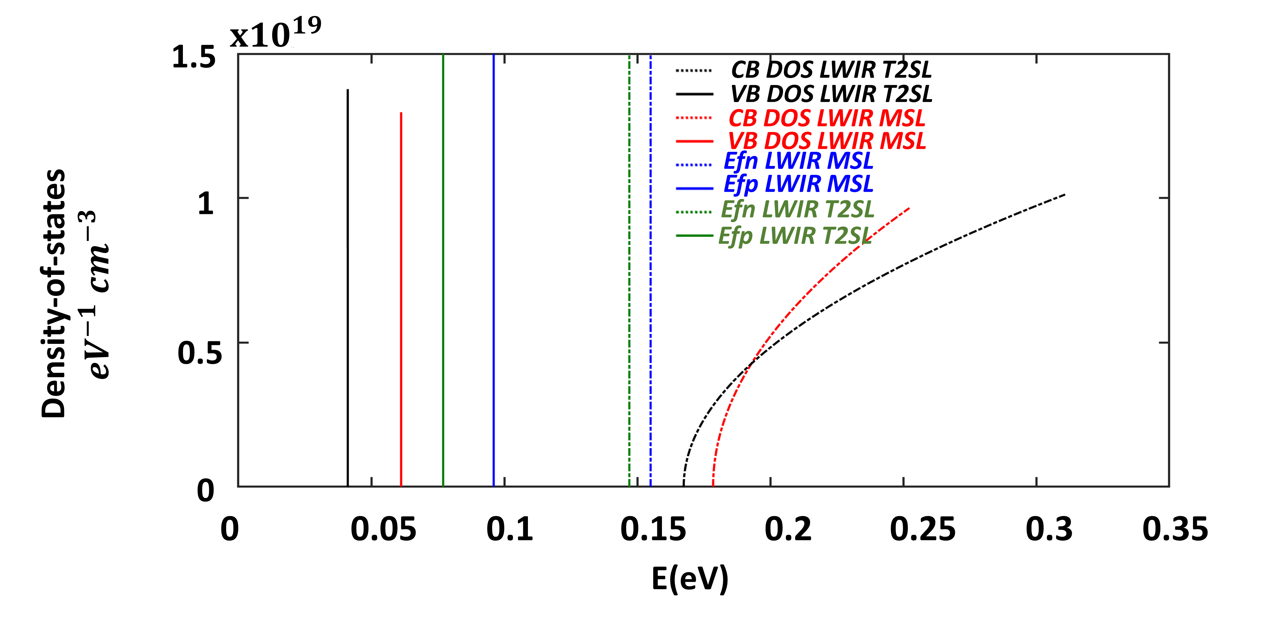
Next, by restricting the conduction miniband width to a lesser than the bandgap of the superlattice, AM-1 Auger recombination can be prohibited as, by the reduction in the miniband width, we remove the possible transition of electrons to the higher energyKitchin et al. (2000); Grein et al. (1995). While there is a reduction in these recombinations in the growth direction they will still be present in the in-plane directionKitchin et al. (2000). The mini bandwidth is 144 and 72 in T2SL and MSL, respectively, as discussed earlier. The LWIR T2SL is more susceptible to AM-1 recombination as bandwidth is higher than the bandgap, which is 0.125. Auger recombination is expected to be suppressed in the MSL since the mini bandwidth is lower than the bandgap in the MSL, as there are no available states to satisfy the energy and momentum conservationGrein et al. (1995). Furthermore, in Fig. 16, we plot the quasi-2D density-of-states for the T2SL and MSL with the quasi-fermi levels corresponding to the acceptor doping of and excess carrier concentration as . We notice that the density of states in MSL is a bit lower than that of states in
T2SL, especially near the Brillouin zone edge (), which further reduces their auger recombination probability in the MSL.
A few more parameters are calculated to compare further these LWIR absorbers, such as the HH-LH split, electron
effective masses, electron and hole effective masses,
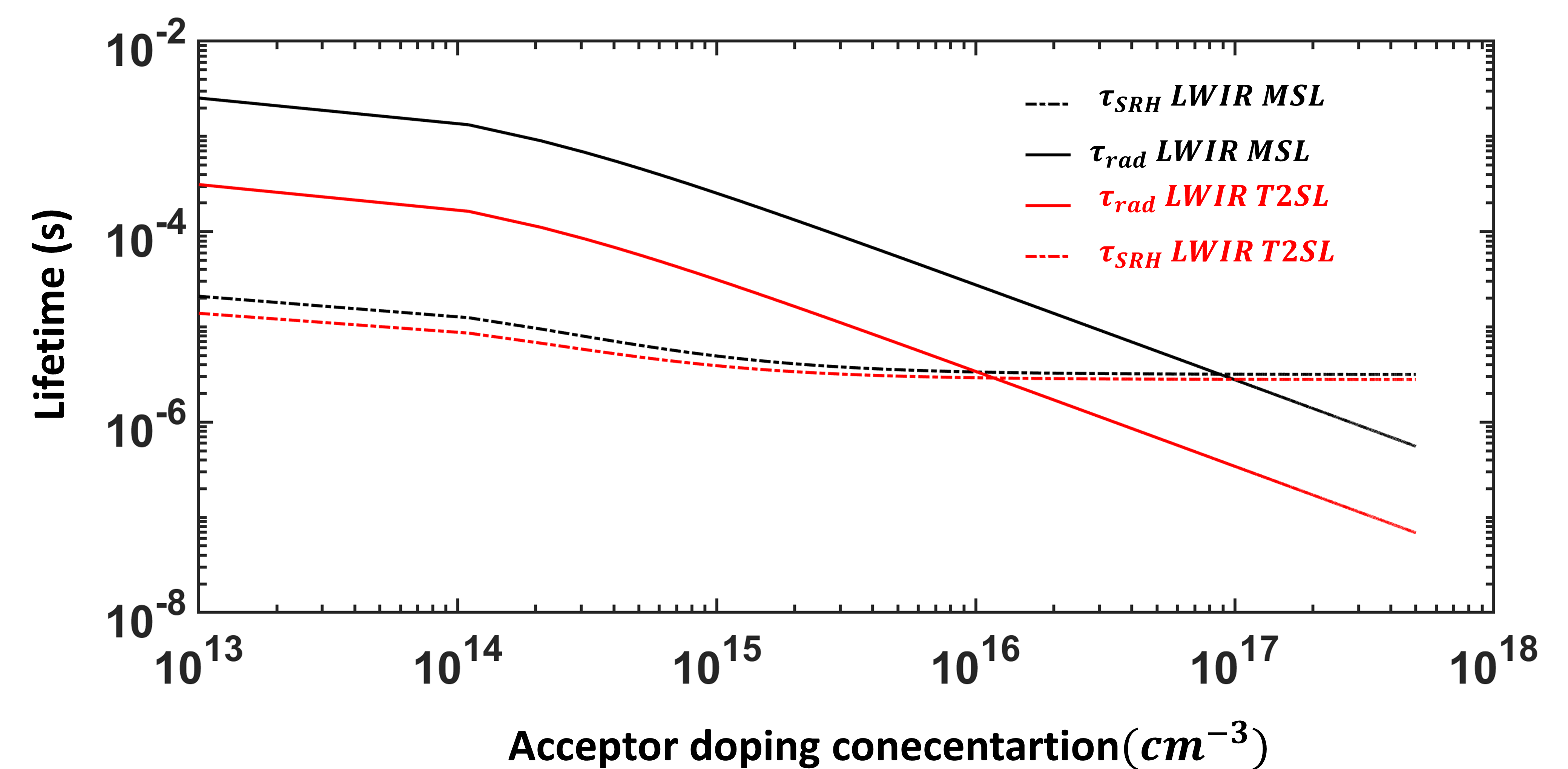
ni and SRH capture coefficients, as shown in Table. 2. In Fig. 16 (b), we plot the SRH and recombination lifetime with the different values of acceptor doping varying from , calculated by the equation. 21 and 22, respectively, by using the parameters calculated in the Table. 2. We have seen that at the lower acceptor doping, the SRH recombination dominates for both T2SL and MSL, while at higher doping levels, it is the radiative process that decides the lifetime of the minority electrons in the p-type () T2SL and MSL. Typically, the SRH lifetime dominates at the lower temperature, but the auger recombination dominates at the higher temperature and higher doping. In the case of MSL, we can achieve higher doping to increase the quantum efficiency,
as it has lesser radiative and Auger recombination rates
and, hence, a higher lifetime.
The absorption gives information about the electron and hole pairs generated in the active region. In the case of the LWIR T2SL, as discussed above, the absorption coefficient of T2SL is higher than the MSL, which may lead to higher quantum efficiency, but due to the higher PL intensity, they are more prone to radiative recombination, and their SRH capture constants are also lower as calculated in Table. 2. Furthermore, as discussed T2SL has a higher Auger recombination probability, which suggests that for LWIR application, MSL could be a better choice as they can be doped higher than the T2SL to increase the quantum efficiency and still contribute less to the dark current.
From Fig.16 (b), the radiative recombination dominates at a higher doping level; therefore, MSL has a higher
carrier lifetime and, hence, higher diffusion length. In the case of T2SL, the generated electron-hole pairs will readily recombine, and there are fewer chances for them to participate in the photocurrent. Whereas, in MSL, as it has a higher diffusion length, a thicker MSL can be taken according to the number of periods that can incorporated while keeping the overall thickness lower than the diffusion length. For example, at , the minority carrier (electron) lifetime is around and for MSL and T2SL, respectively. The diffusion constant length () for MSL is thrice of the T2SL (neglecting the mobility, as effective electron masses are almost similar see; Table. 2). In addition, the absorption increases linearly with the increase in superlattice periods, whereas the sublinear increases in dark currents have been reported Aeberhard (2008). Therefore, a higher thickness of MSL will have better optical absorption and will be less prone to dark currents.
III.1.4 Comparison for MWIR Absorber
In this section, we compare the MWIR T2SL and MSL absorbers, similar to the LWIR absorber for infrared photodetection. For this, 8ML/16ML T2SL and 9ML/4ML/2ML/4ML MSL configurations are taken, with the equivalent bandgap of 0.28 , and the corresponding wavelength is around 4.5 . We plot the electronic band structures of these superlattices in Figs. 17 (a) and (b). The conduction miniband widths are and for T2SL and MSL, respectively. The holes have negligible mini bandwidth, showing dispersion-less characteristics along the growth axis Klipstein et al. (2021). This implies that while heavy holes are extremely localized within the GaSb well, their tunneling transport is less. In contrast, electrons have a wider miniband than heavy holes, and as a result, they contribute to the tunneling current.
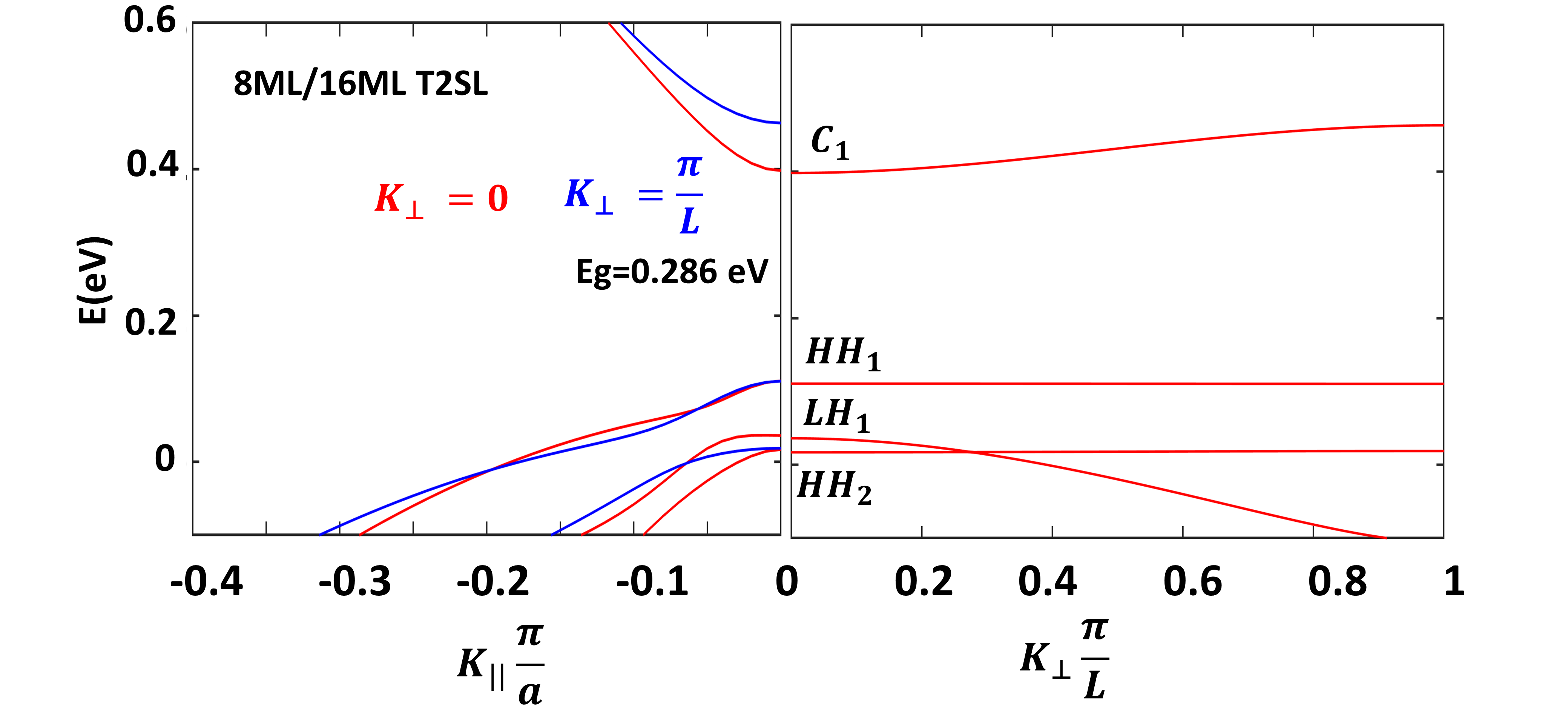
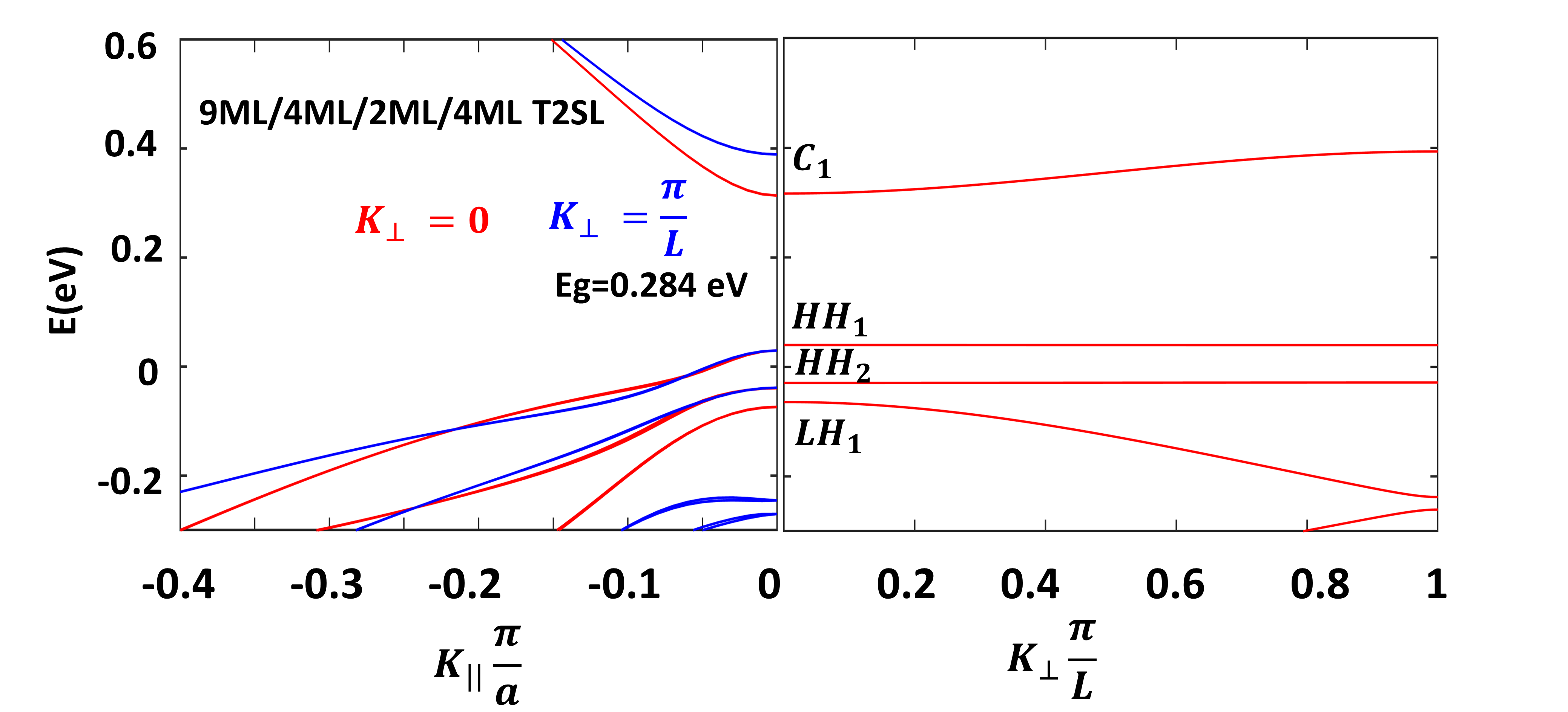
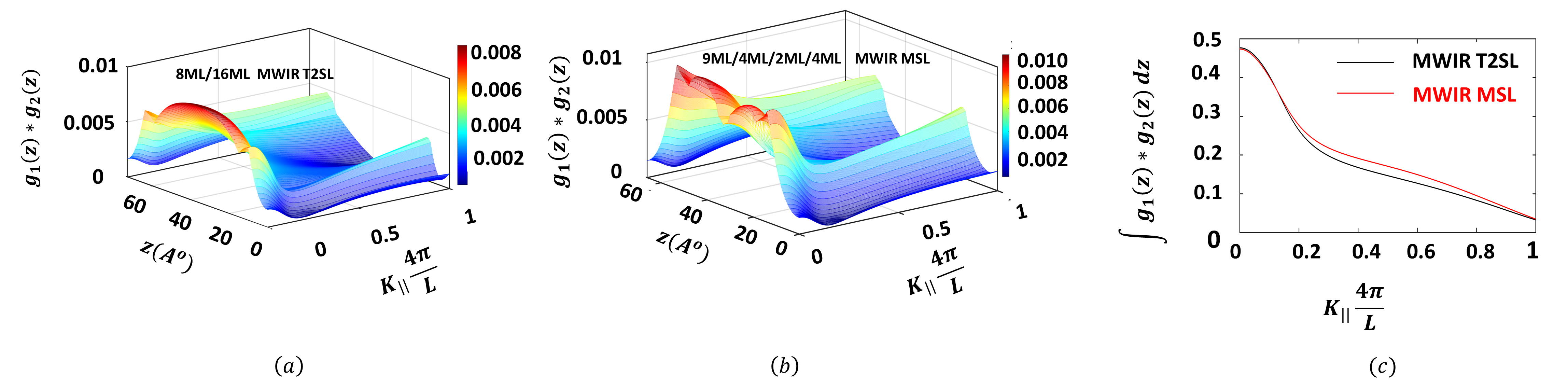
The squared envelope wavefunctions for the , , , and are plotted in Fig.18 (a) and (b) for T2SL and MSL, respectively. The high probability of finding holes in MSL is eminent in newly formed GaSb hole wells. Also, the center of shifts further towards the center of the electronic wavefunction in the InAs well, which results in an increased spatial product of envelope wavefunctions at the interfaces, as shown in Figs. 19 (a) and (b). In this particular case of MSL, notice a higher - wavefunction overlap, as shown in Figs. 19 (a) and (b) at the interfaces. Additionally, we calculate the oscillator strength of the - transition, which dominates the absorption since other bands are located distant from the quasi-fermi levels and contribute less to the absorption. Even when the overlap at the interfaces is larger in the MSL, as in Fig. 19 (b), then in T2SL 19 (a), the calculated oscillator strength in the Fig. 19 (c) is similar for the T2SL and MSL.
| Parameters | T2SL | MSL |
| Bandgap (eV) | 0.286 | 0.284 |
| HH-LH splitting () | 0.0747 | 0.0692 |
| Electron effective mass | 0.0389 | 0.0408 |
| Hole effective mass | 0.2580 | 0.2974 |
| Intrinsic carrier concentration | ||
| Overlap integral value at K=0 (C1-HH1) | 0.4766 | 0.473 |
| Radiative recombination coefficient () | ||
| SRH |
Next, in the Figs. 20 (a) and (b), we plot the optical matrix elements for TE and TM polarization for further inspection of the optical transitions in the MWIR superlattice. At the lower values, the - TE components dominate, while the TM components are practically absent close to the Brillouin zone center Wang et al. (2016). The strongest behavior is seen by the TM components for the - transitionAvrutin et al. (1993). Similar to what was mentioned for the LWIR absorbers, the TE and TM modes exhibit the opposite behavior. While TE for heavy holes and conduction band transitions reduces from higher to lower, TM increases from the zone center to the higher Wang et al. (2016). Near the zone center, the TM component for the - is higher than the TE component.
Additionally, in the case of T2SL, we have seen an antiband crossing of HH2-LH2 at non-zero out-of-plane wavevector, but in the case of MSL, HH2 has shifted above the LH1, and there is an anti-band crossing near the zone center also as shown in Figs. 17 (a) and (b), respectively.
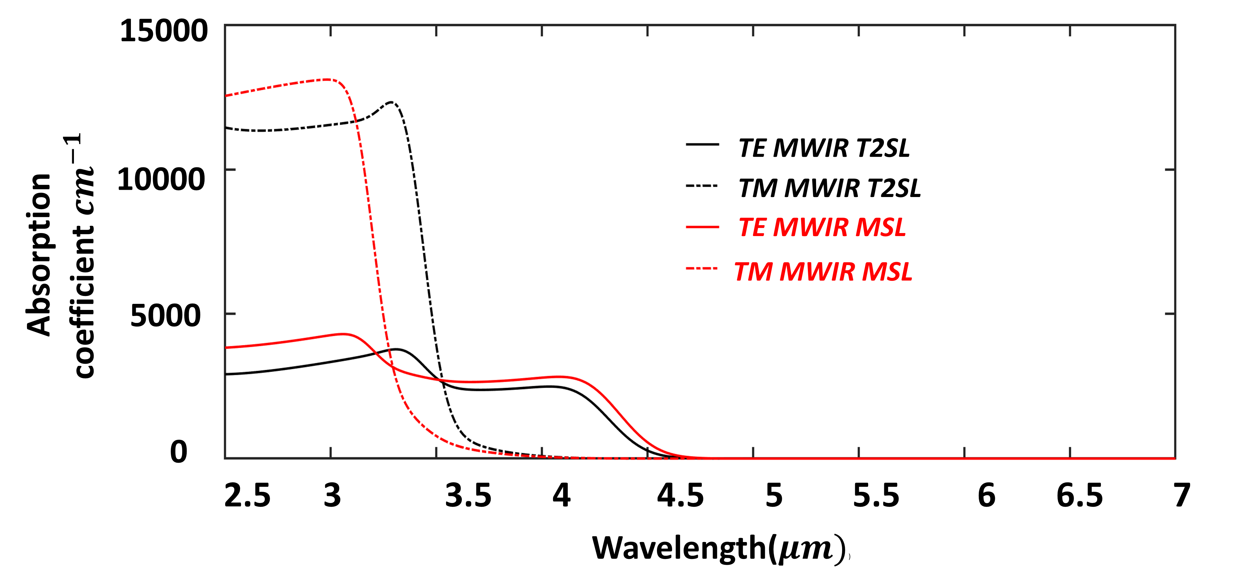
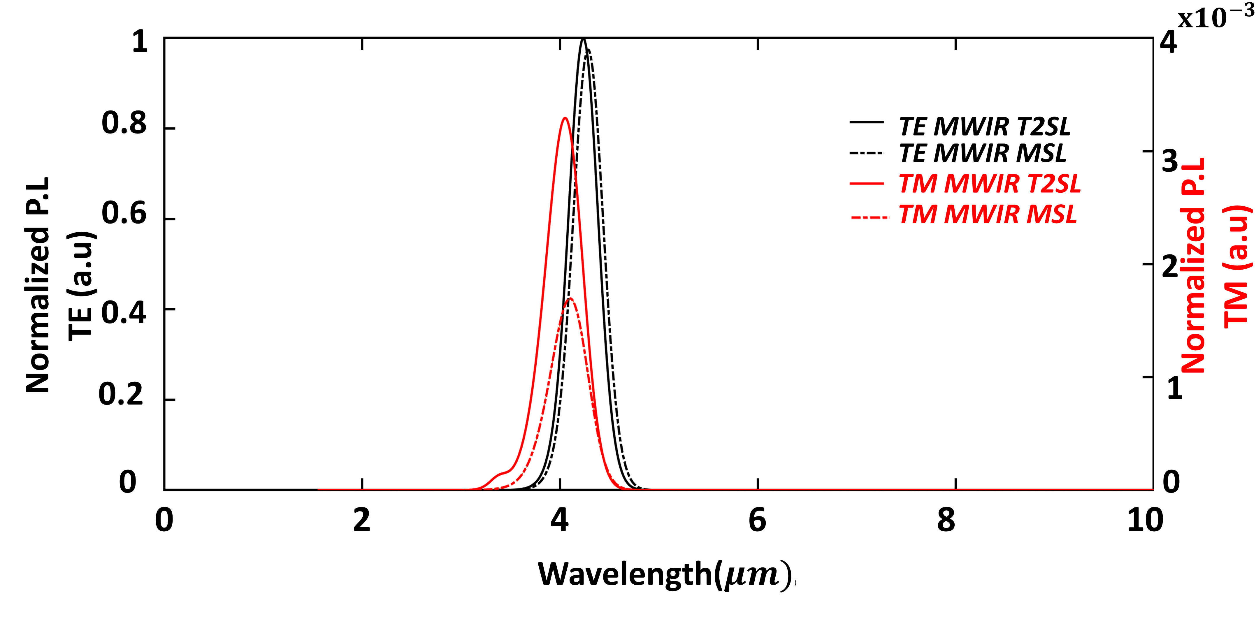
With the help of the obtained moment elements and the quasi-fermi levels at the doping concentration of , we calculate the absorption coefficient at the incident photon energies. It can be seen in Fig. 21 (a) that the TE dominates at higher wavelengths. The contribution of the TE is higher at the lower photon energies due to the dominant C1-HH1 transition, but as the excitation energy rises, the C1-LH1 transition begins to rise and at a certain energy the magnitude of TE and TM absorption are equal, as shown in Fig. 21, and afterward, the TM dominates over the TE Avrutin et al. (1993). Now, we plot the P.L intensity for these superlattices, both for the TE and TM polarization and observe that the TE peak is stronger than the TM peak. We also notice a shift in the TM w.r.t. to the TE peak. This is because the TM - transition rises after a certain .
The TE PL for the T2SL and MSL are approximately the same; however, the TM for the T2SL has been found to be higher. The obtained absorption is plotted in Fig. 21, depicts the higher MSL absorption, whereas the PL spectra for the dominant TE transitions are almost similar for both T2SL and MSL.
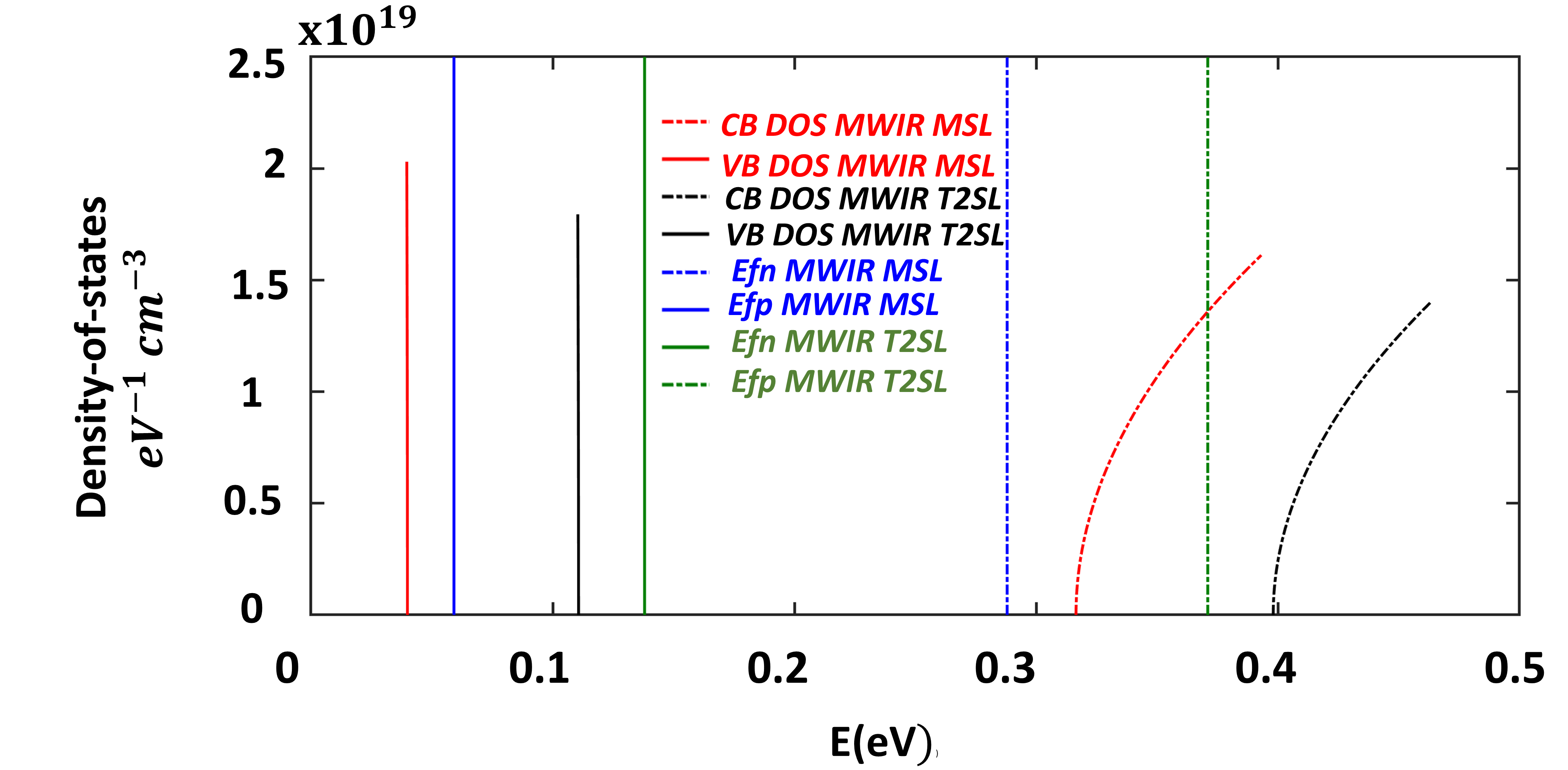
The same conduction miniband width suggests a similar AM-1 auger recombination rate in these superlattices. While the AM-7 will be reduced in MSL, as the - transition probability is less in the case of MSL, as shown in Fig. 20 (c). Later, in Fig.22 (a), we plot the quasi-2D density-of-states for these superlattices with their quasi-fermi levels and observe that MSL has higher density-of-states than in T2SL, especially at the Brillouin zone edge. Therefore, the MSL’s AM-1 auger recombination will
be a bit higher. The calculated radiative and SRH are also similar for these superlattices, as shown in Table. 3.
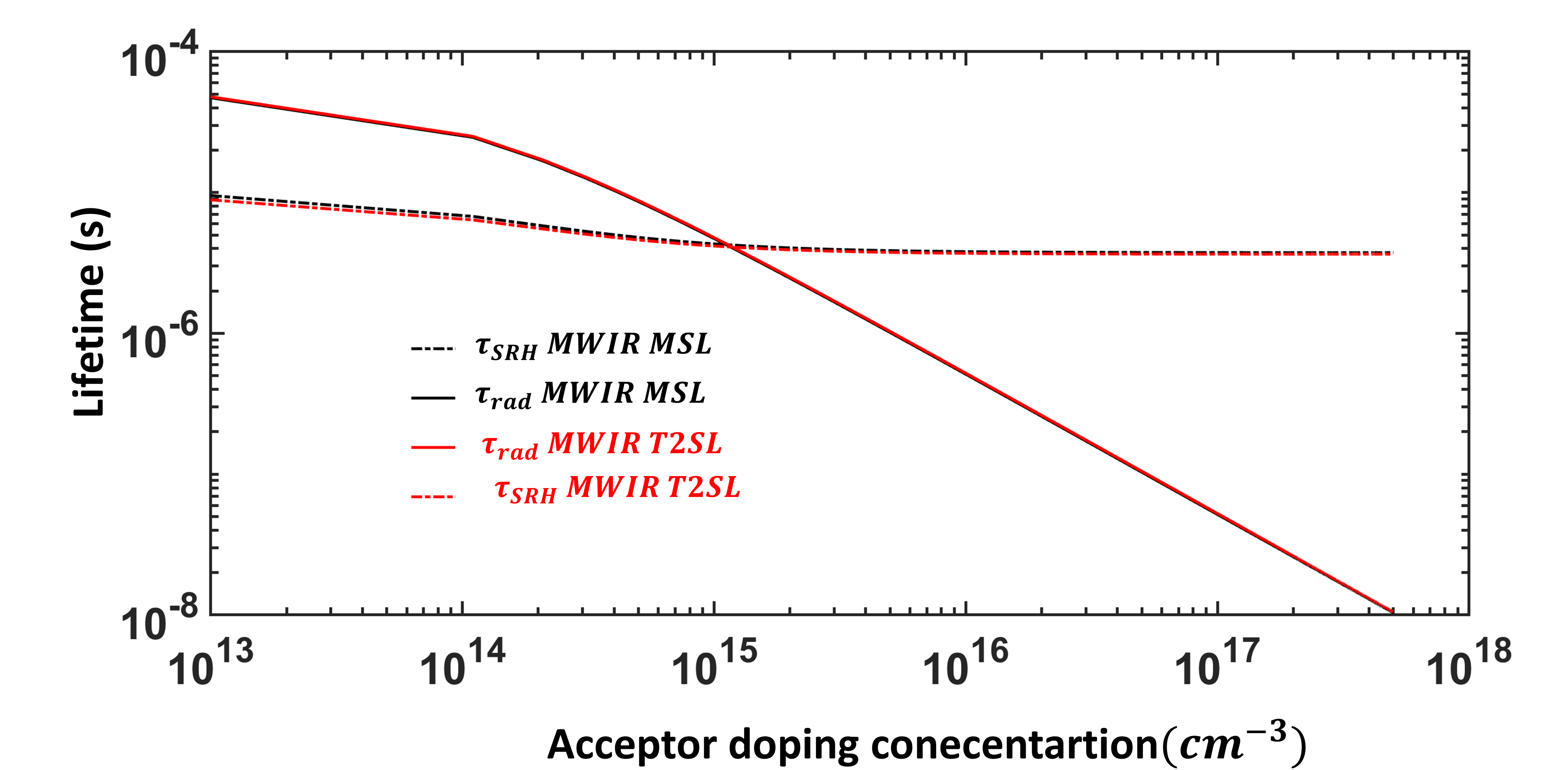
We plot the SRH and radiative recombination for the MWIR T2SL and MSL using the calculated values in Table.3 and equations.21 and .22 in the Fig.22 (b). Here, we notice almost similar lifetime constants for both T2SL and MSL, and the radiative process dominates at higher doping around , and onwards, this doping value is lower than predicted for the LWIR case. In the case of MWIR, the T2SL, and MSL, we observe similar optical and dark current properties, so the additional AlSb layer in the MSL didn’t improve the performance of the MWIR detection as was predicted. However, we were able to achieve the same performance parameters by a thinner period of MSL than the T2SL, which makes it superior to the T2SL for MWIR detection. For example, we calculate the quantum efficiency by at 4.2, where is the absorption coefficient and the L is the thickness of the absorber, and we obtain the quantum efficiency for 2 of T2SL and MSL as 34 and 41 , respectively. Therefore, MSL has improved quantum efficiency in the MWIR region.
III.2 Barrier
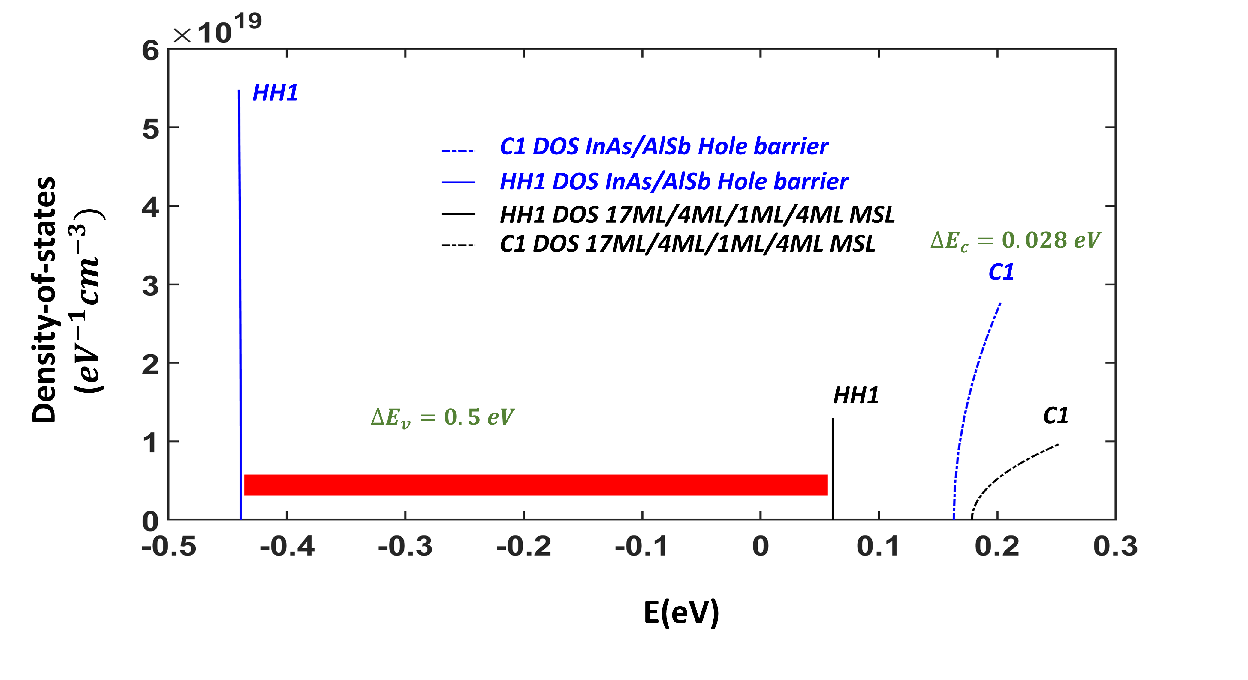
An XBp photodetector consists of three regions: contact, barrier, and active or absorber region. Introducing a barrier in these detectors reduces the SRH and band-to-band tunneling currents; therefore, they perform better than traditional PIN detectorsDelmas et al. (2017). To restrict the flow of carriers from the contact to the active region, which may contribute to the thermionic currents. If not appropriately treated, it may become equal to the diffusion current. Hence, there should be a proper band offset, which prohibits this flow. Not just the band offsets, the doping and the thickness of the barrier corresponding to the absorber region play a crucial role in the dark current flow and carriers’ collection to their respective contacts. Here, we plot the density-of-states for the 12ML/7ML InAs/AlSb hole barrier and for the 17ML/4ML/1ML/4ML LWIR MSL absorber in Fig.23. Here we can observe that the hole barrier provides a valence band offset of around 0.5 for the holes and is almost negligible i.e. 28 conduction band offset w.r.t to the absorberMir and Frensley (2013).
IV Conclusion
An exhaustive study of the InAs/GaSb type-II superlattice and InAs/GaSb/AlSb/GaSb M superlattice has been done to achieve high-operating temperature infrared photodetectors. The 8-band theory, with the inclusion of the InSb layer at the interface, was employed to calculate the band properties. The main results include bandgap variations, oscillator strength, and SRH capture lifetime constants. The absorption spectra of symmetric type-II lattices were calculated by utilizing Fermi’s Golden rule. The absorption and photoluminescence were found to be functions of widths of the InAs and GaSb taken in one period of the superlattice. These calculations also led to the calculation of the radiative recombination coefficient, which was found to be higher for the lower widths of InAs and GaSb. Further, to increase the absorption and diffusion length in the type-II superlattice, we explored the M superlattice. We have studied the effects of introducing the high bandgap AlSb layer on the bandgap, heavy hole-light hole split-off energy, and the possible reason for the red shift in the photoluminescence spectra. On the basis of the carrier localization and carrier spatial overlap at the interface, we have compared the same bandgap type-II and M superlattice. The diffusion length was predicted to be higher in the case of long wavelength M superlattice, as it was less prone to the auger and radiative recombinations. Similar characteristics to the mid-wavelength type-II superlattice have been observed with the thinner M superlattice, which enhanced the quantum efficiency.
Acknowledgment
The authors acknowledge the funding from the PMRF Ph.D. scheme of the Ministry of Education, Government of India, and this work is also supported by ISRO-IIT Bombay Space Technology Cell.
References
- Plis (2014) E. A. Plis, Advances in Electronics 2014 (2014).
- Alshahrani et al. (2022) D. O. Alshahrani, M. Kesaria, E. A. Anyebe, V. Srivastava, and D. L. Huffaker, Advanced Photonics Research 3, 2100094 (2022).
- Rogalski et al. (2017) A. Rogalski, P. Martyniuk, and M. Kopytko, Applied physics reviews 4, 031304 (2017).
- Müller et al. (2020) R. Müller, M. Haertelt, J. Niemasz, K. Schwarz, V. Daumer, Y. V. Flores, R. Ostendorf, and R. Rehm, Micromachines 11, 1124 (2020).
- Zhu et al. (2021) H. Zhu, J. Liu, H. Zhu, Y. Huai, M. Li, Z. Liu, and Y. Huang, in Photonics, Vol. 8 (MDPI, 2021) p. 564.
- Mohseni et al. (1999) H. Mohseni, J. Wojkowski, M. Razeghi, G. Brown, and W. Mitchel, IEEE journal of quantum electronics 35, 1041 (1999).
- Delmas et al. (2023) M. Delmas, D. Ramos, R. Ivanov, L. Žurauskaitė, D. Evans, D. Rihtnesberg, S. Almqvist, S. Becanovic, E. Costard, and L. Höglund, Opto-Electronics Review 31 (2023).
- Maimon and Wicks (2006) S. Maimon and G. Wicks, Applied Physics Letters 89, 151109 (2006).
- Singh et al. (2022) A. Singh, S. Mukherjee, and B. Muralidharan, Journal of Applied Physics 131, 094303 (2022).
- Delmas et al. (2019) M. Delmas, B. Liang, and D. L. Huffaker, in Quantum Sensing and Nano Electronics and Photonics XVI, Vol. 10926 (International Society for Optics and Photonics, 2019) p. 109260G.
- Boutramine et al. (2016) A. Boutramine, A. Nafidi, D. Barkissy, E.-S. El-Frikhe, H. Charifi, A. Elanique, and H. Chaib, Applied Physics A 122, 1 (2016).
- Lang and Xia (2011) X.-L. Lang and J.-B. Xia, Journal of Physics D: Applied Physics 44, 425103 (2011).
- Lang and Xia (2013) X.-L. Lang and J.-B. Xia, Journal of Applied Physics 113, 043715 (2013).
- Mukherjee et al. (2021) S. Mukherjee, A. Singh, A. Bodhankar, and B. Muralidharan, Journal of Physics D: Applied Physics 54, 345104 (2021).
- Huang et al. (2011) E. K.-w. Huang, A. Haddadi, G. Chen, B.-M. Nguyen, M.-A. Hoang, R. McClintock, M. Stegall, and M. Razeghi, Optics letters 36, 2560 (2011).
- Razeghi and Nguyen (2010) M. Razeghi and B.-M. Nguyen, Physics Procedia 3, 1207 (2010).
- Nguyen et al. (2010) B.-M. Nguyen, S. A. Pour, S. Bogdanov, and M. Razeghi, in Quantum Sensing and Nanophotonic Devices VII, Vol. 7608 (SPIE, 2010) pp. 659–667.
- Zhu et al. (2022) X. Zhu, W. Jie, Y. Lyu, Z. Peng, J. Wang, Y. He, M. Li, L. Zhang, and Z. Ji, Applied Physics A 128, 599 (2022).
- Fang et al. (2022) S. Fang, R. Hao, L. Zhang, J. Guo, and W. Liu, Frontiers in Physics 10, 822800 (2022).
- Nghiem et al. (2017) J. Nghiem, E. Giard, M. Delmas, J. Rodriguez, P. Christol, M. Caes, H. Martijn, E. Costard, and I. Ribet-Mohamed, in International Conference on Space Optics—ICSO 2016, Vol. 10562 (SPIE, 2017) pp. 1159–1167.
- Ting et al. (2020) D. Z. Ting, S. B. Rafol, A. Khoshakhlagh, A. Soibel, S. A. Keo, A. M. Fisher, B. J. Pepper, C. J. Hill, and S. D. Gunapala, Micromachines 11, 958 (2020).
- Sharma et al. (2021) A. Sharma, J. Kedia, and N. Gupta, Optical Engineering 60, 090901 (2021).
- Li et al. (2010) L. Li, W. Xu, and F. Peeters, Physical Review B 82, 235422 (2010).
- Galeriu (2005) C. Galeriu, PhD Disertations. Worcester Polytechnic Institute, Worcester , 16 (2005).
- Shulenberger et al. (2023) K. E. Shulenberger, M. R. Jilek, S. J. Sherman, B. T. Hohman, and G. Dukovic, Chemical Reviews 123, 3852 (2023).
- Szmulowicz et al. (2006) F. Szmulowicz, H. Haugan, G. Brown, K. Mahalingam, B. Ullrich, S. Munshi, and L. Grazulis, Opto-Electronics Review 14, 69 (2006).
- Alshahrani et al. (2023) D. Alshahrani, M. Kesaria, J. J. Jiménez, D. Kwan, V. Srivastava, M. Delmas, F. M. Morales, B. Liang, and D. Huffaker, ACS Applied Materials & Interfaces 15, 8624 (2023).
- Livneh et al. (2012) Y. Livneh, P. Klipstein, O. Klin, N. Snapi, S. Grossman, A. Glozman, and E. Weiss, Physical Review B 86, 235311 (2012).
- Klipstein et al. (2021) P. Klipstein, Y. Benny, Y. Cohen, N. Fraenkel, R. Fraenkel, S. Gliksman, A. Glozman, I. Hirsch, O. Klin, L. Langof, et al., in Infrared Technology and Applications XLVII, Vol. 11741 (SPIE, 2021) pp. 102–112.
- Höglund et al. (2013) L. Höglund, D. Ting, A. Khoshakhlagh, A. Soibel, C. Hill, A. Fisher, S. Keo, and S. Gunapala, Applied Physics Letters 103 (2013).
- Olson et al. (2015) B. V. Olson, E. A. Kadlec, J. K. Kim, J. F. Klem, S. D. Hawkins, E. A. Shaner, and M. E. Flatte, Physical Review Applied 3, 044010 (2015).
- Trupke et al. (2003) T. Trupke, M. A. Green, P. Würfel, P. Altermatt, A. Wang, J. Zhao, and R. Corkish, Journal of Applied Physics 94, 4930 (2003).
- Brown et al. (2006) G. Brown, H. Haugan, F. Szmulowicz, K. Mahalingam, S. Munshi, B. Ullrich, and S. Houston, in Quantum Sensing and Nanophotonic Devices III, Vol. 6127 (SPIE, 2006) pp. 381–392.
- Dyksik et al. (2017) M. Dyksik, M. Motyka, M. Kurka, K. Ryczko, J. Misiewicz, A. Schade, M. Kamp, S. Höfling, and G. Sęk, Japanese Journal of Applied Physics 56, 110301 (2017).
- Qiao et al. (2012) P.-F. Qiao, S. Mou, and S. L. Chuang, Optics express 20, 2319 (2012).
- Wang et al. (2016) W. Wang, H. Lu, L. Fu, C. He, M. Wang, N. Tang, F. Xu, T. Yu, W. Ge, and B. Shen, Optics express 24, 18176 (2016).
- Ahmed (2016) M. Ahmed, (2016).
- Subashiev et al. (2004) A. Subashiev, L. Gerchikov, and A. Ipatov, Journal of applied physics 96, 1511 (2004).
- Kitchin et al. (2000) M. Kitchin, M. Shaw, E. Corbin, J. Hagon, and M. Jaros, Physical Review B 61, 8375 (2000).
- Grein et al. (1995) C. Grein, P. Young, M. Flatté, and H. Ehrenreich, Journal of Applied Physics 78, 7143 (1995).
- Azarhoosh et al. (2016) P. Azarhoosh, S. McKechnie, J. M. Frost, A. Walsh, and M. Van Schilfgaarde, Apl Materials 4 (2016).
- Seyedein Ardebili et al. (2023) S. B. Seyedein Ardebili, J. S. Kim, J. Ha, T. I. Kang, B. Zeinalvand Farzin, Y. Kim, and S. J. Lee, Energies 16, 1162 (2023).
- Benchtaber et al. (2020) N. Benchtaber, A. Nafidi, D. Barkissy, A. Boutramine, M. Benaadad, S. Melkoud, E.-S. Es-Salhi, and F. Chibane, Frontiers in Physics 8, 52 (2020).
- Benaadad et al. (2021) M. Benaadad, A. Nafidi, S. Melkoud, A. Boutramine, et al., in E3S Web of Conferences, Vol. 229 (EDP Sciences, 2021) p. 01036.
- Hussain et al. (2022) G. Hussain, G. Cuono, R. Islam, A. Trajnerowicz, J. Jureńczyk, C. Autieri, and T. Dietl, Journal of Physics D: Applied Physics 55, 495301 (2022).
- Ting et al. (2011) D. Z. Ting, A. Soibel, B. Rafol, J. Nguyen, L. Höglund, A. Khoshakhlagh, S. A. Keo, J. K. Liu, J. M. Mumolo, and S. D. Gunapala, in Infrared Technology and Applications XXXVII, Vol. 8012 (SPIE, 2011) pp. 391–400.
- Imbert et al. (2015) J. Imbert, V. Trinite, S. Derelle, J. Jaeck, E. Giard, M. Delmas, M. Carras, R. Haidar, J. Rodriguez, and P. Christol, Infrared Physics & Technology 70, 81 (2015).
- Singh and Muralidharan (2022) A. Singh and B. Muralidharan, in Optical Sensing and Detection VII, Vol. 12139 (SPIE, 2022).
- Nguyen et al. (2009) B.-M. Nguyen, S. Bogdanov, S. A. Pour, and M. Razeghi, Applied Physics Letters 95, 183502 (2009).
- Akhavan et al. (2016) N. D. Akhavan, G. A. Umana-Membreno, R. Gu, M. Asadnia, J. Antoszewski, and L. Faraone, IEEE Transactions on Electron Devices 63, 4811 (2016).
- Mukherjee and Muralidharan (2018) S. Mukherjee and B. Muralidharan, Integrated Ferroelectrics 194, 37 (2018).
- Kopytko et al. (2015) M. Kopytko, J. Wróbel, K. Jóźwikowski, A. Rogalski, J. Antoszewski, N. Akhavan, G. A. Umana-Membreno, L. Faraone, and C. Becker, Journal of Electronic Materials 44, 158 (2015).
- Li et al. (2019) Y. Li, W. Xiao, L. Wu, X. Xie, P. Lu, and S. Wang, in 2019 IEEE 4th Optoelectronics Global Conference (OGC) (IEEE, 2019) pp. 70–75.
- Downs and Vandervelde (2013) C. Downs and T. E. Vandervelde, Sensors 13, 5054 (2013).
- Das et al. (2023) S. Das, J. Dutta, S. D. Gupta, G. Jayaswal, and M. K. Hooda, JOSA B 40, 789 (2023).
- Aytac et al. (2016) Y. Aytac, B. Olson, J. Kim, E. Shaner, S. Hawkins, J. Klem, M. Flatté, and T. Boggess, Physical Review Applied 5, 054016 (2016).
- Klein (2014) B. Klein, Defect investigations in InAs/GaSb type-II strained layer superlattice (The University of New Mexico, 2014).
- Aytac et al. (2015) Y. Aytac, B. Olson, J. Kim, E. Shaner, S. Hawkins, J. Klem, M. Flatté, and T. Boggess, in Quantum Sensing and Nanophotonic Devices XII, Vol. 9370 (SPIE, 2015) pp. 80–87.
- Connelly et al. (2010) B. C. Connelly, G. D. Metcalfe, H. Shen, and M. Wraback, Applied physics letters 97 (2010).
- Andreev and Subashiev (2002) A. Andreev and A. Subashiev, Physica E: Low-dimensional Systems and Nanostructures 13, 556 (2002).
- Magri and Zunger (2000) R. Magri and A. Zunger, Physical Review B 62, 10364 (2000).
- Aeberhard (2008) U. Aeberhard, A microscopic theory of quantum well photovoltaics, Ph.D. thesis, ETH Zurich (2008).
- Avrutin et al. (1993) E. Avrutin, I. Chebunina, I. Eliachevitch, S. Gurevich, M. Portnoi, and G. Shtengel, Semiconductor science and technology 8, 80 (1993).
- Delmas et al. (2017) M. Delmas, R. Rossignol, J. Rodriguez, and P. Christol, Superlattices and Microstructures 104, 402 (2017).
- Mir and Frensley (2013) R. N. Mir and W. R. Frensley, Journal of Applied Physics 114 (2013).