Molecular beam epitaxy growth of superconducting tantalum germanide
Abstract
Developing new material platforms for use in superconductor-semiconductor hybrid structures is desirable due to limitations caused by intrinsic microwave losses present in commonly used III/V material systems. With the recent reports that tantalum provides drastic improvements when implemented in superconducting circuit elements over traditional Nb and Al films, exploring Ta as an alternative superconductor in hybrid material systems seems necessary. Here, we present our study on the growth of Ta on semiconducting Ge (001) substrates grown via molecular beam epitaxy. We show that the Ta diffuses into the Ge matrix in a self-limiting nature resulting in extremely smooth and abrupt surfaces and interfaces that are ideal for future cQED device fabrication. The films have a nominal composition of TaGe2 and form a native oxide of nominal composition Ta2Ge2O5 that also forms a sharp interface with the underlying film. These films are superconducting with a K and , .
Superconductor-semiconductor (S-Sm) hybrid material platforms have been of interest in the last few decades for studying mesoscopic superconductor physics Rahman et al. (1996), the search for topological superconductivity Mourik et al. (2012); Prada et al. (2020), and most recently for the development of new voltage-tunable qubits, couplers, and other superconducting circuit elements Casparis et al. (2018); Burkard et al. (2020); Strickland et al. (2022). However, due to the complexity of the material requirements (e.g. interface roughness, band alignment, etc.), growth of these structures is not straightforward. Furthermore, in terms of the latter application in superconducting circuitry for circuit quantum electrodynamics (cQED) applications, high intrinsic losses in the community standard Al-InAs system Casparis et al. (2018) have motivated material exploration studies to search for materials better suited towards these cQED applications. On the other hand, recent advancements in the Si-Ge alloy system present these materials to be highly promising for low-microwave loss materials Sandberg et al. (2021); Scappucci et al. (2021) for quantum information applications.
In terms of superconducting materials, implementation of tantalum metal is also extremely interesting for cQED devices due to the fact that it forms a well-behaved native oxide for superconducting microwave applications Shen (1972); Spencer and Rowell (1981); Face et al. (1986). Additionally, recent studies showed that this behavior of Ta also propagates to high-performance cQED devicesPlace et al. (2021); McLellan et al. (2023). In this context, major increases in qubit coherence times are caused by low intrinsic two-level system (TLS) losses within the Ta metal native oxide, Ta2O5. However, implementation of this material into S-Sm hybrid materials requires significant effort in terms of understanding the film growth parameters to promote smooth interfaces/surfaces. Thus, further study of Ta and Ta-alloys is of interest for investigation of new superconductor-semiconductor (S-Sm) hybrid material systems.
Here, we report the first diffusion-limited growth (diffusion-growth) of tantalum germanide films via molecular beam epitaxy (MBE). We evaluate our grown films via a suite of structural and electronic materials characterization and present the chemical composition, structure, and superconductivity behavior of this material. We present a unique growth method that forms uniform, wafer-scale thin films of homogeneous chemical composition and thickness that make this material system highly promising for future application in superconducting cQED devices.
The tantalum germanide films are grown on 50.8mm Ge(001) substrates in a custom solid-source molecular beam epitaxy system (Mod Gen II) equipped with three electron beam sources and hydrogen cleaning capabilities. The internal manifold around the sources is water-cooled and no L cryo-paneling is used during this deposition. The substrates are first etched ex-situ in deionized water at 90∘C for 15 minutes and then immediately loaded into vacuum on indium-free blocks. The substrates are initially outgased in the growth reactor at 200∘C for 15 minutes, before slowly increasing temperature to 550∘C to anneal for 10 minutes. Ta deposition was done using a water-cooled vertical EBVV e-beam source from MBE Komponenten at an emission current of 180mA in a 6kV acceleration field. The films are grown at 400∘C, immediately following the Ge oxide removal. Due to passive heating from the Ta source, deposition was conducted in three cycles of 10 minutes each, allowing the chamber to cool for 15 minutes between deposition cycles to prevent significant outgasing from the chamber walls.
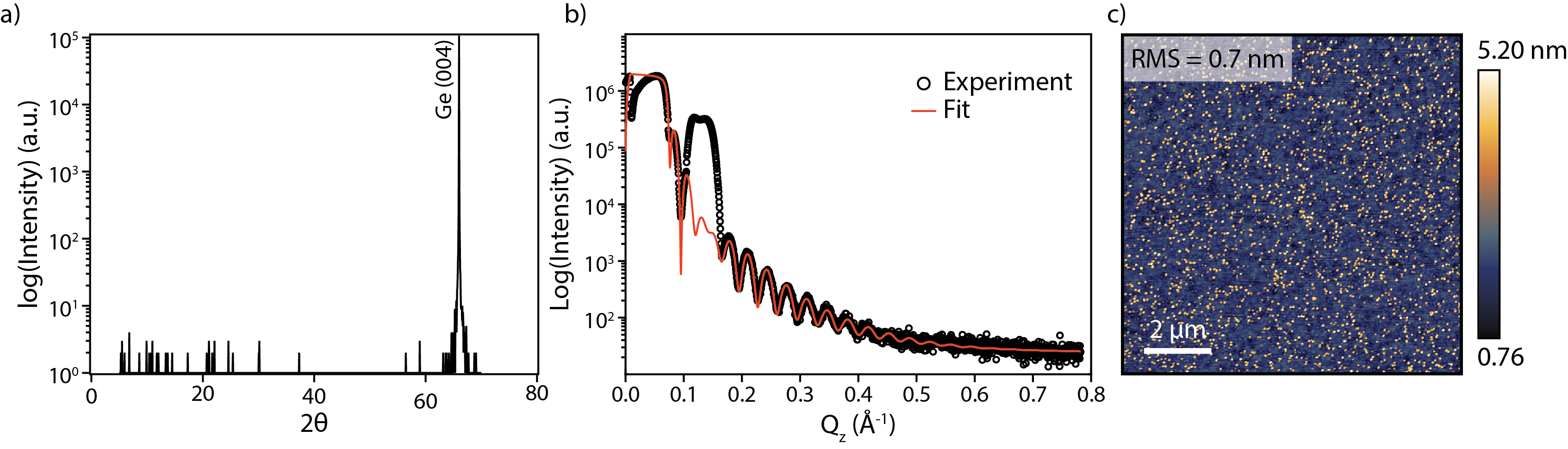
Figure 1 presents x-ray diffraction data taken using a Bruker D8 Discovery lab source diffractometer with a da Vinci configuration and a conditioned Cu K source. A collimator and 1mm slit are used to reduce the effects of substrate bowing in select measurements. All scans are measured in a double crystal configuration. An out-of-plane scan is presented in Fig. 1a in which the only reflection visible is the substrate Ge (004) reflection at 66deg. X-ray reflectivity (XRR) measurements are taken after removing the collimator and reducing the slits to 0.2mm. The XRR results are presented in Figure 1b, showing extremely sharp interfaces for the amorphous film. The fit is initialized assuming a two-layer model for the film structure with the primary layer being a film of tantalum germanide and the secondary layer being a thin native oxide layer. Since the density is unknown due to the amorphous nature, we allow the scattering length density (SLD) to vary in the fitting procedure as well. The results of the fit are shown below in table 1. The feature that is not captured by our fitting model we speculate is related to the dot-like features observed in the atomic force microscopy (AFM) image seen in Figure 1c. These features are well dispersed across the sample surface and are all nominally a uniform thickness and may be the cause of this spurious peak that is not captured by our two-layer model. The roughness values for the fits are initialized at 7 , the roughness we measured in AFM, but then is allowed to vary for both layers individually.
| Layer | SLD () | thickness () | Roughness () |
|---|---|---|---|
| Tantalum Germanide | 93.97 | 175.1 | 3.6 |
| Native Oxide | 64.95 | 24.4 | 9.3 |
From the fits we extract scattering length densities (SLD) for total internal reflection x-ray scattering in the XRR measurements. Using Eqn. 1 below we then calculate the product of , relating the SLD from the fit back to the material density and scattering factor.
| (1) |
Where is the material density, is Avogadro’s constant, is the classical electron radius m, is the molar mass, and is the real part of the atomic scattering factor of the compound. We calculate values of and for the tantalum germanide and native oxide layers, respectively.
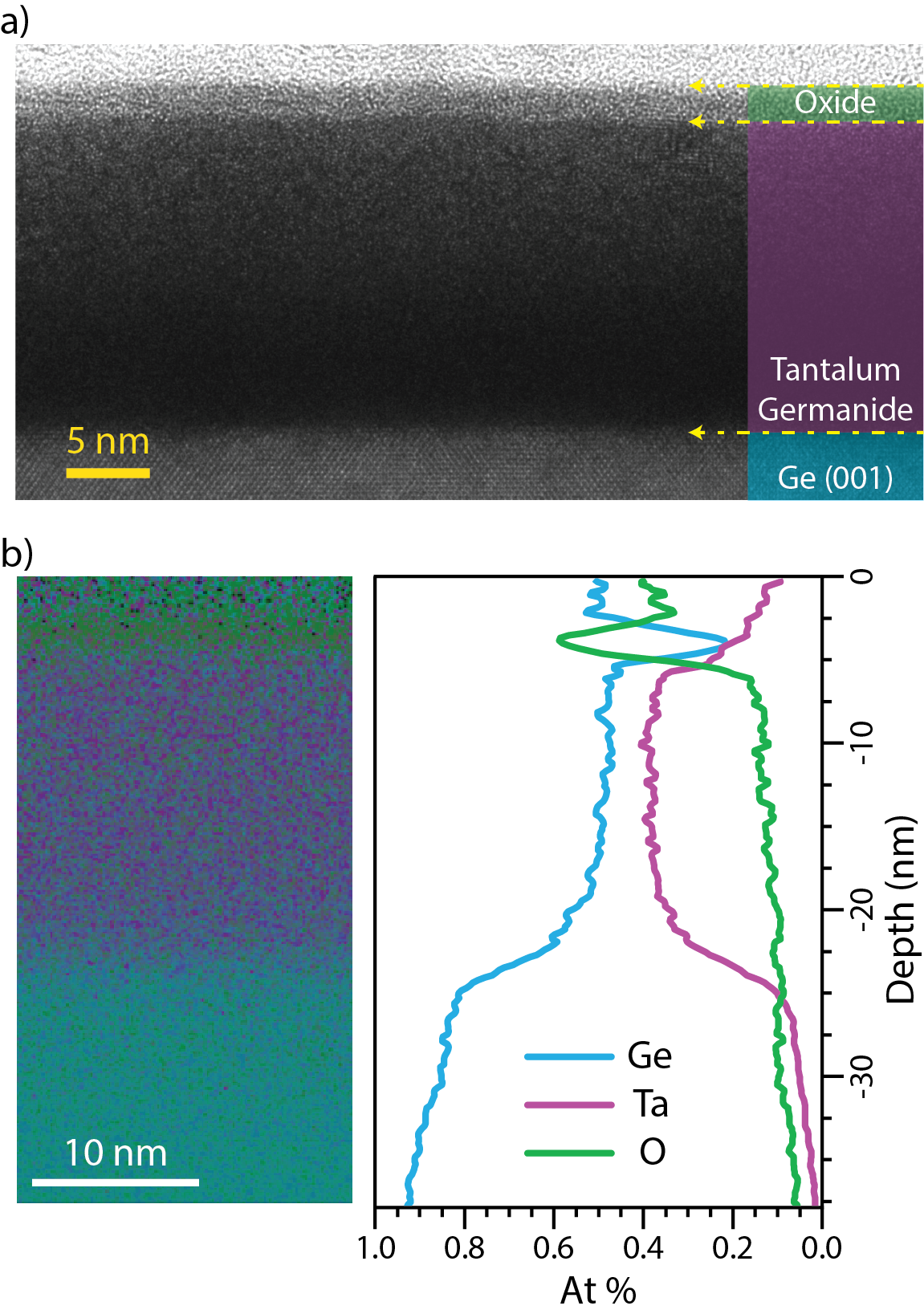
Crystallinity and composition of the tantalum germanide film is examined with scanning transmission electron microscopy (STEM) in a JEOL ARM200F, equipped with a spherical aberration corrector for probe mode, and operated at 200 keV. The samples were prepared with cross-sectional tripod polishing to 20 m thickness, followed by shallow angle Ar+ ion milling with low beam energies([1]3 keV), and LN2 stage cooling in a PIPS II ion mill. Exemplary transmission electron microscopy images are shown in Figure 2, where we observe sharp interfaces and well-defined film and oxide regions of thicknesses 18.7nm and 2.2nm, respectively, in good agreement with our XRR fitting. To calculate the material density, rough estimations of film composition are obtained from energy dispersive x-ray spectroscopy (EDS) as shown in Figure 2b. From EDS we estimate the tantalum germanide phase to be Ta:Ge ratio and the native oxide to have a composition of O:Ta:Ge. From these compositions we see that the film and native oxide layers have approximate chemical formulations of TaGe2 and Ta2Ge2O9, respectively. Interestingly, this implies that the oxide is made up of a mixture of one part Ta2O5 and two parts GeO2.
Assuming random distribution of elemental species in the two distinct layers, we then calculate average material densities to be and for the TaGe2 and oxide layers, respectively. We attribute the larger density than reported literature values for TaGe2 ( Brixner (1963)) to a Ta-rich phase, likely due to small regions of non-reacted Ta metal. Interestingly, the calculated density of the oxide layer is significantly larger than reports of Ta2O5 and GeO2, which are 8.31 Stephenson and Roth (1971) and 6.27 Baur and Khan (1971), respectively. However, there are reports of high pressure phases of the tantalum pentaoxide in which the densities are drastically increased Zibrov et al. (2000) up to . Therefore, we speculate the nature of this oxide layer to be the result of residual internal strains inducing the formation of small regions of high density polymorphs of the Ta2O5 and GeO2 native oxide phases.
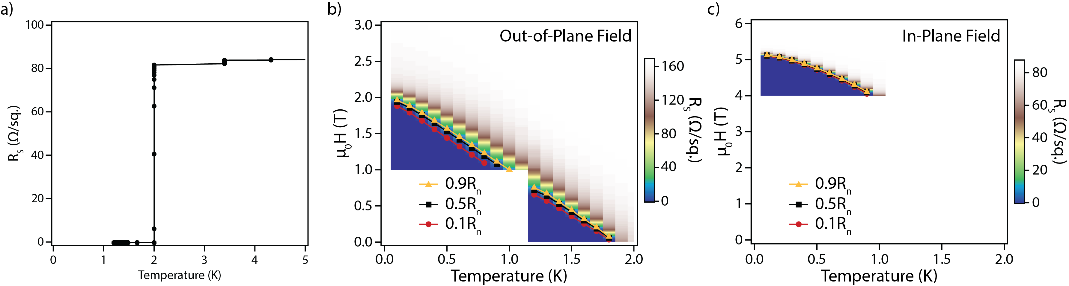
Magnetotransport measurements of this material are done in an Oxford Triton dry dilution refridgerator with a base temperature of 15mK and a single direction magnet with a maximum field of 14T. Samples are cleaved down to roughly 5x5mm chips. Contacts on the chip are made by annealing In-Sn eutectic into the four corners in a Van der Pauw geometry which are then contacted to the sample board via gold wires. The results of these measurements are presented in Figure 3. We see a sharp transition to a zero resistance state at roughly 2K upon cooldown, as shown in Figure 3a. To investigate the field dependance, we sweep out-of-plane and in-plane magnetic field as shown in Figs. 3b and c, respectively. The resistance surface presented in Fig. 3b shows a very sharp transition from the superconducting phase to the normal state, suggestive of type 1 superconductivity. This is observed in the tight spread of 0.9Rn, 0.5Rn, and 0.1Rn contours overlaid on the color map. For out-of-plane field configuration we observe a critical applied field of . The critical field fitting gives us a critical temperature of roughly 1.8K. With an in-plane field configuration we measure a critical applied field of that also exhibits a sharp superconducting transition up to 1K. We present this data in Fig. 3c in which we overlay the 0.9Rn, 0.5Rn, and 0.1Rn contours. The variation in sheet resistance between Fig. 3b and Figs. 3a and c are a result of oxidation in the film over the course of roughly six months causing a slight increase in film resistance. The measurements were otherwise conducted on the exact same sample.
In conclusion, we presented here the growth, structure, and transport characteristics of diffusion-grown tantalum germanide thin films grown via MBE. The tantalum germanide films are formed by a rate-limited diffusion process in which the e-beam evaporated Ta diffuses into the surface such that a nominal composition of of is maintained within the film region. These films form a small native oxide layer with sharp interfaces that has a composition that suggests the formation of both and , also in a ratio of . Transport shows a reasonable critical temperature of 1.8-2K, but more we find a critical out-of-plane and in-plane critical field of and , respectively. With such a high critical field and the ease of semiconductor integration, this new superconducting material is interesting to study cQED devices.
Acknowledgements.
The authors would like to acknowledge funding support for this project by AFOSR award FA9550-21-1-0338.References
- Rahman et al. (1996) F. Rahman, T. J. Thornton, R. Huber, L. F. Cohen, W. T. Yuen, and R. A. Stradling, “Superconductor-semiconductor interaction effects in mesoscopic hybrid structures,” Phys. Rev. B 54, 14026–14031 (1996).
- Mourik et al. (2012) V. Mourik, K. Zuo, S. M. Frolov, S. R. Plissard, E. P. A. M. Bakkers, and L. P. Kouwenhoven, “Signatures of majorana fermions in hybrid superconductor-semiconductor nanowire devices,” Science 336, 1003–1007 (2012).
- Prada et al. (2020) E. Prada, P. San-Jose, M. W. A. de Moor, A. Geresdi, E. J. H. Lee, J. Klinovaja, D. Loss, J. Nygåd, R. Aguado, and L. P. Kouwenhoven, “From andreev to majorana bound state in hybrid superconductor-semiconductor nanowires,” Nat. Rev. Phys. 2, 575–594 (2020).
- Casparis et al. (2018) L. Casparis, M. R. Connolly, M. Kjaergaard, N. J. Pearson, A. Kringhøj, T. W. Larsen, F. Kuemmeth, T. Wang, C. Thomas, S. Gronin, G. C. Gardner, M. J. Manfra, C. M. Marcus, and K. D. Petersson, “Superconducting gatemon qubit based on a proximitized two-dimensional electron gas,” Nat. Nanotechnol. 13, 915–919 (2018).
- Burkard et al. (2020) G. Burkard, M. J. Gullans, X. Mi, and J. R. Petta, “Superconductor-semiconductor hybrid-circuit quantum electrodynamics,” Nat. Rev. Phys. 2, 129–140 (2020).
- Strickland et al. (2022) W. M. Strickland, B. H. Elfeky, J. O. Yuan, W. F. Schiela, P. Yu, D. Langone, M. G. Vavilov, V. E. Manucharyan, and J. Shabani, “Superconducting resonators with voltage-controlled frequency and nonlinearity,” Phys. Rev. Appl. 19, 034021 (2022).
- Sandberg et al. (2021) M. Sandberg, V. P. Adiga, M. Brink, C. Kurter, C. Murray, M. Hopstaken, J. Bruley, J. S. Orcutt, and H. Paik, “Investigating microwave loss of sige using superconducting transmon qubits,” Appl. Phys. Lett. 118, 124001 (2021).
- Scappucci et al. (2021) G. Scappucci, C. Kloeffel, F. A. Zwanenburg, D. Loss, M. Myronov, J.-J. Zhang, S. D. De Franceschi, G. Katsaros, and M. Veldhorst, “The germanium quantum information route,” Nat. Rev. Mater. 6, 926–943 (2021).
- Shen (1972) L. Y. L. Shen, Superconductivity in d- and f-Band Metals, edited by D. H. Douglass (Springer, 1972).
- Spencer and Rowell (1981) E. G. Spencer and J. M. Rowell, “Superconductivity of ta-zr films produced by co-sputtering,” IEEE Trans. Magn. MAG-17, 322–325 (1981).
- Face et al. (1986) D. W. Face, D. E. Prober, W. R. McGrath, and P. Richard, “High quality tantalum superconducting tunnel junctions for microwave mixing in the quantum limit,” Appl. Phys. Lett. 48, 1098–1100 (1986).
- Place et al. (2021) A. P. M. Place, L. V. H. Rodgers, P. Mundada, B. M. Smitham, M. Fitzpatrick, Z. Leng, A. Premkumar, J. Bryon, A. Vrajitoarea, S. Sussman, G. Cheng, T. Madhavan, H. K. Babla, X. H. Le, Y. Gang, B. Jäck, A. Gyenis, N. Yao, R. J. Cava, N. P. de Leon, and A. A. Houck, “New material platform for superconducting transmon qubits wit coherence times exceeding 0.3 milliseconds,” Nat. Commun. 12, 1779 (2021).
- McLellan et al. (2023) R. A. McLellan, A. Dutta, C. Zhou, Y. Jia, C. Weiland, X. Gui, A. P. M. Place, K. D. Crowley, X. H. Le, T. Madhavan, Y. Gang, L. Baker, A. R. Head, I. Waluyo, R. Li, K. Kisslinger, A. Hunt, I. Jarrige, S. A. Lyon, A. M. Barbour, R. J. Cava, A. A. Houck, S. L. Hulbert, M. Liu, A. L. Walter, and N. P. de Leon, “Chemical profiles of the oxides on tantalum in state of the art superconducting circuits,” Advanced Science 10, 2300921 (2023).
- Vignaud and Gibaud (2019) G. Vignaud and A. Gibaud, “REFLEX: a program for the analysis of specular X-ray and neutron reflectivity data,” J. Appl. Cryst. 52, 201–213 (2019).
- Brixner (1963) L. H. Brixner, “X-ray study and thermoelectric properties of the NbSixGe2-x and the TaSixGe2-x systems,” J. Inorg. Nucl. Chem. 25, 257–260 (1963).
- Stephenson and Roth (1971) N. C. Stephenson and R. S. Roth, “Structural Systematics in the Binary System Ta2O5-WO3. V. The Structure of the Low-Temperature Form of Tantalum Oxide L-Ta2O5,” Acta Cryst. B27, 1037–1044 (1971).
- Baur and Khan (1971) W. H. Baur and A. A. Khan, “Rutile-Type Compounds. IV. SiO2, GeO2 and a Comparison with other Rutile-Type Structures,” Acta Cryst. B27, 2133–2139 (1971).
- Zibrov et al. (2000) I. P. Zibrov, V. P. Filonenko, M. Sundberg, and P.-E. Werner, “Structures and phase trasitions of B-Ta2O5 and Z-Ta2O5: two high-pressure forms of Ta2O5,” Acta Crys. B56, 659–665 (2000).