Interplay between strain and size quantization in a class of topological insulators based on inverted-band semiconductors
Abstract
We consider surface states in semiconductors with inverted-band structures, such as -Sn and HgTe. The main interest is the interplay of the effect of a strain of an arbitrary sign and that of the sample finite size. We clarify the origin of various transitions which happen at a given strain with the change of the sample thickness, in particular the transition between the Dirac semimetal and quasi-3D (quantized) topological insulator. We compare our results with the ones recently published in the literature. For the k-p Kane model we derive effective boundary conditions in the case when the direct band materials form high barriers for the carriers of the inner inverted-band semiconductor (for example, CdTe/HgTe/CdTe and CdTe/-Sn/CdTe cases). We show that in this case the BCs have an universal and simple form which does not depend on the order of different non-commuting operators in the Hamiltonian. Even in the limit of very high barriers the BCs do not reduce to the trivial zero form, but contain the information about the asymmetry of the offsets in the conduction and valence bands. These boundary conditions allow to investigate the realistic case of finite mass of the heavy hole band, and to compare the results obtained within the Kane and the Luttinger models.
I Introduction
Describing the electronic band structure of gapless semiconductors has long been an interesting problem because of the rich physics at their interfaces. Gapless semiconductors, like HgTe (or -Sn), have inverted band structures where the s-like () and p-like ( ) bands switch order in energy due primarily to strong spin-orbit coupling. Groves ; Bloom ; Gelmont Crystalline symmetry enforces a four-fold degeneracy at the -point, effectively closing the bandgap. Because of the band inversion, interfaces with vacuum or with direct band-gap semiconductors having ordinary band ordering can produce new types of interface (surface) states, namely Dyakonov-Khaetskii (DK) states Dyak and Volkov-Pankratov (VP) states Volkov ; Cade ; Suris ; Volkov1 . Moreover, these surface states have nondegenerate spin-texture, making them interesting for spintronics and optoelectronics applications. Ando Though these surface states were postulated in the 1980s, their properties remain consistent with what can be expected from topological phases of materials. Hasan ; Qi ; Bernevig ; Kane ; Dai ; Khaetskii ; Pankratov Experimentally, these interface states can be revealed by angle- and spin-resolved photoemission spectroscopy Xia ; Hsieh and magneto-transport measurements. Brune ; Kozlov ; Checkelsky ; Analytis ; Ren ; Xia1 ; Pan
The energy dispersion of interface states becomes more complex for many practical samples of a thin topological insulator deposited onto a topologically trivial semiconductor or insulator. Under these circumstances, both finite-size effects and epitaxial strain can significantly modify the electronic band structure, causing transitions between different topological states. Because future devices employing topological materials will likely be made using thin films, the interplay of the finite-size effects and strain within a topological insulator is an important and interesting problem. In the current literature, there is a broad range of opinions about the origin and exact conditions for topological transitions of thin-film TIs Ohtsubo ; Coster ; Anh . The main goal of this work is to understand the physics of the series of transitions that happen at a given strain value with changing sample width.
We consider here a model system comprised of a gapless semiconductor with an inverted band structure (e.g. HgTe or -Sn) of finite-width sandwiched between layers of a direct-gap (DG) semiconductor (e.g. CdTe or InSb), see Fig. 1. In section II, we present the Hamiltonian of the Kane model which includes also the contributions from the far bands; thus the HH band acquires a finite mass, which allows one to describe the physics applicable for realistic situations. In section III we develop the necessary boundary conditions (BCs) for a proper solution under finite thickness. In the case when the direct-band materials form high barriers for the carriers of the inner inverted-band semiconductor the BCs have an universal and simple form, thereby offering simple analytical treatment and more physical insight than achieved previously. In section IV we use these BCs within the Kane model with strain and finite HH mass to describe the interface between the inverted-band and direct-band semiconductors focusing on the energies of the DK surface states Dyak ; Khaetskii . This problem is important because of the necessity to clarify existing ARPES data. In section V we introduce finite-size effects and show how they split the VP states and discuss how it relates to possible interpretations of experimental data (for example, ARPES). Finally, in section VI, we describe the interplay between strain and finite-size effects for cases of biaxially compressive and tensile strain.
II Material Configuration and Hamiltonian
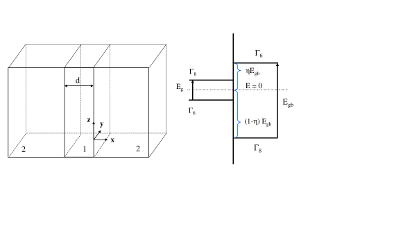
In this paper we consider several cases related to surface states of a semi-infinite sample or quantized states when one deals with a thin film or QW. In all cases we have a contact of an inverted-band semiconductor (of the -Sn type) with a direct-band semiconductor (like CdTe, for example) or vacuum. Actual calculations for a finite size sample will be done for the case of symmetric structure of the type CdTe/-Sn/CdTe.
The band structures of both the direct and inverted-band semiconductors are described by the Kane model which takes into account three bands: electrons (e) with s-like symmetry, light holes (lh) with p-type symmetry, and heavy holes (hh) also with p-type symmetry. Using the time-reversal symmetry of the problem and choosing the proper coordinate system reduces the problem to the one Subashiev ; Khaetskii . We choose the angular momentum quantization axis z in the plane of the interface and the direction of the carrier motion along y; x denotes the direction normal to the interface. With this coordinate system, the two groups of states (e 1/2, lh -1/2, hh 3/2) and (e -1/2, lh 1/2, hh -3/2) do not mix. The Hamiltonian matrix for the first group of states, see Refs. (Subashiev, ,Bir, ), after the use of the unitary transformation
| (1) |
acquires the following form:
| (2) |
The Hamiltonian matrix that refers to the second group of states with the opposite sign of the angular momentum projection on the z-axis can be obtained from Eq.(2) by replacing by . In Eq.(2) is the Kane matrix element which we consider coordinate-independent; are second-order valence band Luttinger parameters, which have different values in a gapless semiconductor 1 and in a direct semiconductor 2; and are conduction and valence band edge energies (in the absence of strain) in semiconductors 1 and 2, respectively. Strain is applied to the inverted-band semiconductor 1, in practice through an epitaxial constraint. is the strain-induced gap energy between the light and heavy hole bands and can have either sign, .
A solution of the equation in the bulk case (translation invariance) leads to the equation:
| (3) |
Here , and . Throughout the paper we assume the quantities and in both materials to be positive. Equation (3) determines the bulk spectra of three types of particles: electrons, light holes, and heavy holes. At zero strain (), when heavy holes are decoupled, the spectra have the usual, relatively simple form that is determined by equating two factors on the left hand side of Eq. (3) to zero. Note that at , when a motion of particles is perpendicular to the interface, the heavy holes are also decoupled from the light particles (i.e., electrons and light holes).
III Boundary conditions
III.1 High-energy barriers between inverted and direct materials
The wave functions (spinors) in all regions have the form
| (7) |
Here corresponds to the electron contribution, while and describe the light-hole and heavy-hole contributions, respectively. We will consider further (except subsection III, C) the case of high-energy offsets in the conduction and valence bands where the energy gap of the direct barrier material is large compared to the energy gap of the inverted-band material. Using this condition we find the following decaying solutions in the barrier region, , for the heavy and light particles:
| (14) |
Function Eq.(7) in the barrier region is a linear superposition of the functions Eq.(14). Here , and . The parameter () describes the asymmetry of the offsets in the conduction and valence bands, see Fig. 1. The edges of the conduction and valence bands in the barrier region are and , where is the energy gap of the direct-gap (barrier) material. The zero of the energy coincides with the middle of the gap of the inverted material. The case corresponds to symmetric offsets.
III.2 Boundary conditions
While deriving the boundary conditions, we will consider the lowest-order effects in small , where is the energy gap in the inverted-band material. Consequently, one takes into account the finite values of and only in the heavy holes spectrum, thus the flat HH band acquires a finite mass. Assuming the high barrier condition, one obtains the following effective boundary conditions for the wave function inside the gapless material 1, see Fig. 1:
| (15) |
We note that at the opposite boundary () the sign in front of the imaginary unity in Eq. (15) should be changed for the negative one. By the effective boundary conditions we mean the following. With high barriers condition we can consider the solution of the Schrodinger equation only in the inner region 1, all the information about the barrier regions enters the problem through the BCs presented by Eq. (15). In this way we avoid the usual troubles Bastard related to the choice of the order of different noncommuting operators in the Hamiltonian, Eq. (2). It is remarkable that even in the limit of very high barriers the BCs do not reduce to the trivial zero form (), but contain the information about the asymmetry of the offsets in the conduction and valence bands. It is also important to mention that while considering the surface states problem with high-energy barriers and for energies near the point (i.e. much smaller than the energy gap ) one can neglect the contribution from the electron band. Then the boundary conditions within the Luttinger model reduce to , i.e. to zero values of the light-hole and heavy-hole components Dyak ; Dyak1 .
III.3 Location of the Dirac point of the Volkov-Pankratov states (a single interface)
For arbitrary values of the gap energies, , in the inverted and direct (barrier) materials, and arbitrary offsets in the conduction and valence bands, the exact formula for the location of the Dirac point of the Volkov-Pankratov states Volkov reads
| (16) |
Eq. (16) is obtained from the boundary conditions (continuity of all components of spinors found at in the inverted-band and direct-gap materials, while neglecting the terms).
Some ARPES experiments Engel show that the DP lies in close proximity to the point. This location can be obtained from Eq.16 in the case when and . means that the offset in the conduction band is much larger than in the valence band. Then at one obtains , i.e. at the energy of the point of the inverted material.
If, however, one considers the case of -Sn/InSb interface Engel , then using the values of offsets from Ref. Cardona, and assuming a zero strain, one obtains the location of the DP to be rather closer to the middle of the -Sn gap, which differs from the interpretations Engel of the ARPES measurements.
It is not clear if Eq. (16) has an analogue in the case the boundary is with vacuum. Interestingly, the authors of Ref. C. Liu, claimed that a strong reconstruction of the surface Z. Lu occurs for their bulk HgTe when bounded by vacuum which leads to the opening of a large gap between the light and heavy-hole bands. Mathematically it is equivalent to the presence of a big positive strain . Such a big positive strain can indeed push the DP towards the top of the heavy-hole band.
IV Kane model with strain and finite heavy-hole mass
The surface state spectrum near the energy for the realistic case of the finite heavy-hole mass is interesting because of the necessity to clarify existing ARPES data Engel . It is especially important to exclude or confirm the possibility of forming the twinning of Dirac cones,Seixas ; Balatsky which we set out to do here for our particular system.
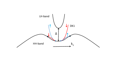
Two types of surface branches are found within the Kane model. The parabolic branch (called DK1 state) Dyak ; Khaetskii starts from the HH band and ends at the LH band. The Volkov-Pankratov states lie within the gap Volkov . The DK1 branch in the presence of strain was studied in Ref. Khaetskii, for the idealized case of a flat heavy-hole band. Here we investigate this problem at (biaxial, in-plane tensile) and for a small ratio of the light and heavy hole masses given by , . We will use the perturbation approach with respect to .
We consider the case of a single interface with a high-energy barrier between the inverted-band and direct band semiconductors. In the lowest order with respect to small (or equivalently ) the spinors in the inverted-band region for the light and heavy particles have the form
| (23) |
Using the boundary conditions in Eq. (15), one obtains the folowing equation for the surface states spectra (for the symmetric case of ):
| (26) |
The quantity in Eqs. (23,26) is defined as . The equation for the time-reversed branch of the states is obtained by replacing by in Eq. (26).
For , using the formulas from Ref. Khaetskii, we find for the exact spectra of the surface branches DK1 which lie above the bottom of the HH band:
| (27) |
where is the energy of the bottom of the HH band, and is the location of the Dirac point of the Volkov-Pankratov states (at ). We should mention that in contrast to the case, for a finite positive strain there are two DK1 branches corresponding to the opposite spins for a given value of . The one corresponding to the spin-up state (for ) exists only up to the critical value of (assuming that ), where it merges with the heavy-hole band, see Fig. 2 and the discussion below.
For completeness we also present here (at ) the exact spectra of two V-P surface branches that lie within the energy gap (and which we derived using the formulas from Ref. Khaetskii, ):
| (28) |
Note that Eq. (28) is the generalization for the case of of the equations of Ref. Volkov1, . Now we solve Eq. (26), looking for by the perturbation theory in small ; for that we use the expression Eq.(27) while calculating the factor . We consider the case . Then for quantity it is enough to use a simple expression . Using the notation , and assuming (which actually means that ), we obtain the desired spectrum of the DK1 surface branch
| (29) |
Here . We will consider the case of small , then two characteristic momenta and relate as . The first one, , is the cut-off value at which the spin-down DK1 branch starts splitting off the HH band, see Fig. 2. (At the quantity , Eq. 26, is not real). We remind that for case the starting point was zero value Khaetskii . At large values of this branch is described by the first line of Eq. (27).
The second branch of surface states in this energy interval near the point corresponds to the spin-up state and is obtained by changing the sign of in Eq. (29). This branch (at ) also starts near (with slight shift from this point determined by small quantity ), has nonmonotonic behavior, and merges again with the heavy-hole band at the point , Fig. 2. This branch exists within the Kane model already in the case of , see the second line of Eq. (27). Since the interval of -values at which it shows up is narrow and is determined by a small strain value, we did not describe this branch in our previous work, Ref. Khaetskii, . (Note that within the Luttinger model, when , this spin-up branch (at ) disappears and Fig. 2 reduces to Fig. 6(b) of Ref. Khaetskii, ). Thus, based on the results obtained here (Fig. 2), we can exclude the formation of a twin Dirac cone for the system we consider.
A similar consideration for the case leads to the spectrum
Here . We note that this branch proceeds up to the point since the edge of the bulk heavy-hole band in this case is described by the equation (i.e. goes down with from the very beginning).
V Gap in the V-P states for the finite-size sample
Above we have considered several problems with the use of the boundary conditions Eq. (15) in the case of a single interface. We have found, in particular, the location of the Dirac point of the Volkov-Pankratov states as a function of the bands’ parameters of the neighbouring materials. A gap is expected to open in the VP states in the case when a film width is finite because of a hybridization of the states belonging to the opposite boundaries. This quantity is also important for the interpretation of the ARPES data. We now consider the effects of finite size on the gap value and spectrum of the VP states. We will be interested in the VP states spectra for small values of , at least , thus we can neglect the interaction with the heavy holes. For simplicity we consider also the zero strain case. Under these conditions, from Eq. (2) of Ref. Khaetskii, we obtain the following two-band model Hamiltonian
| (30) |
For the film of the width with the high barriers one obtains the following equation for the V-P surface states spectrum
| (31) |
In the limit of infinite width , and the solution of the quadratic Eq. (31) reads
| (32) |
It is interesting that the velocities of the V-P branches depend on the parameter which describes the asymmetry of the offsets in the conduction and valence bands. In the limit of large width , the solution is and the spectrum is
| (33) |
Thus in this limit the gap value is exponentially small with respect to the film width. For the derivation of Eq. (33) see Appendix A. Eq. (33) shows that reducing leads to the opening of a gap in these states with the upper branch increasing in energy and the lower branch decreasing, see also Fig. 3 of the Ref. Subashiev, . One can say that the location of the central point of the V-P branches stays at rest within the first-order approximation, but a gap opens between the two Dirac cones, see Appendix A.
It is important to realize what happens near the critical width when the upper branch of the Volkov-Pankratov states ( branch in Fig. 4 of Ref. Subashiev, ) is inverted with the sub-band, which is the first quantized sub-band of the heavy holes. Near this width the energy spectrum (Fig. 4(b) of Ref. Subashiev, ) will look like a linear-in- Dirac dependence with no gap (see also Ref. Dietl, ). One might erroneously conclude that near this energy one has Volkov-Pankratov states with DP close to the point. To the contrary, the lower branch of the Volkov-Pankratov states (i.e. branch, see Figs. (3,4) of Ref. Subashiev, ) lies well below this energy, and the DP also lies below. Note that at (see Fig. 4(b) of Ref. Subashiev, ) the inverted state coincides with the DK1 surface state at . For the details see Ref. Dyak1, .
VI Interplay between the finite size effects and applied strain (surface states within Luttinger model)
We consider here some physics related to the interplay between the finite size effects and applied strain. The important questions can be answered already within the Luttinger model, while considering the characteristic energies near the point. Moreover, the essential physics can be studied within the model with high barriers and zero boundary conditions (i.e. the exact form of the BCs is not important). Everywhere in this section the origin of the energy is at the point. We consider a film of the width with a center of inversion (identical boundaries). We note that all solutions are doubly degenerate with respect to spin because of inversion symmetry. As a measure of topological protection of the surface states at opposite boundaries, one can choose to consider , where is the following overlap integral
| (34) |
where are the states in the quantum well omitting the Bloch exponent . The state in Eq. (34) is chosen from the same block of the Hamiltonian as the state and hence the spinor structure of the two considered states at opposite boundaries is alike noteintegral .
VI.1 Positive (biaxially tensile in-plane) strain,
We begin with the case of positive strain when for a semi-infinite sample one has a 3D topological insulator regime. We now consider what happens with a reduction of the sample size . The limiting cases of and were studied before, and the pictures for these cases are presented in Figs. 6(b) of Ref. Khaetskii, and Fig. 2 of Ref. Dyak1, , respectively.
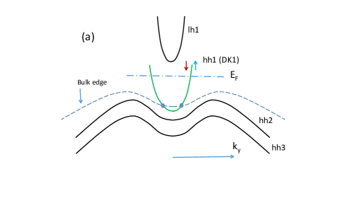
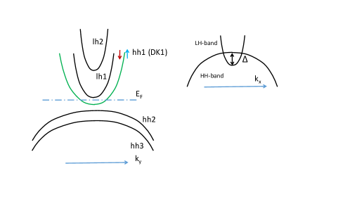
Let us consider first the limit of large width , when the typical quantization energy of light or heavy holes is small compared to the strain-induced gap, . Here and are bulk masses of light and heavy holes. The light and heavy-hole bulk states form a set of sub-bands, see Fig. 3(a). A key point is that for any finite width the quantized states can exist at arbitrary values of in-plane momentum , up to zero value. This differs from the semi-infinite case described above where the DK1 surface branch ceases to exist at some critical value (see Fig. 2 of the present paper and Fig. 6(b) of Ref. Khaetskii, ). This difference is due to the fact that zero boundary conditions on both boundaries of a finite sample can be satisfied with the functions of the form .
As a result, the DK1 branch is transformed into the first heavy-hole subband , see Fig. 3. This transformation occurs at the value which is found from the condition (the expression for and the exact equation for obtained from this condition are given in Appendix B by Eq. (41) and Eq. (40), respectively). At this point the DK1 state crosses the edge of the bulk heavy-hole band. One can also say that at the point the heavy-hole components of the state transform from the form (localized near the center of the film) to the exponents which are localized more near the boundaries (i.e. bulk-like state transforms into the DK1 surface state), see also Ref. Dyak1, .
Allowed values of transverse momenta at are and the corresponding energies of the light and heavy-hole subbands are and , respectively, see Fig. 3.
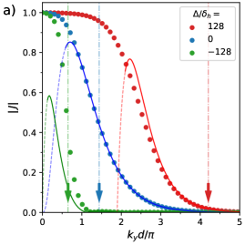
The parameter which determines the crossover between the regimes with an exponentially small value of and the value of is . (Everywhere in this section we assume ). At large width such that Fig. 3 (a) describes a material which still can be treated as a 3D topological insulator. For that, the Fermi level should lie within the branch above the edge of the bulk heavy-hole band (shown by the dashed line) and below the bottom of the sub-band. There are no bulk states at the Fermi level for this situation, besides the overlap of the surface DK1 states belonging to the opposite boundaries is exponentially small since . This case of a big strain corresponds to the red curve of Fig. 4, where the overlap integral of two DK1 surface states localized near the opposite surfaces and having opposite vectors is plotted as a function of for HgTe. The maximally allowed value of () corresponding to the energy of the bottom of the sub-band is shown by the red arrow. We see that for parameters corresponding to the red curve (which can be realized for realistic values of strain only for relatively wide films ) one has the lowest value of the overlap integral .
For thinner films the value of will be much larger. The red curve will become closer to the blue one corresponding to zero strain, and from being proportional to at large (and large ) will change with decreasing tending to . For example, for a width and the strain value corresponding to the parameter is around 40, and the overlap integral value for a maximally allowed is . (Here is the heavy-hole quantization energy, ).
We note that at zero strain while keeping the Fermi level location below the bottom of the sub-band one always has , and since for the DK1 state the length of the localization near the boundary is Dyak , the value of is automatically of the order of unity.
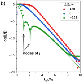
Note that with increasing the positive strain value the overlap integral increases (the red curve versus a blue one) which is quite a counterintuitive behavior. To understand it we note that in the case of exponentially small overlap one has the following analytical expression for (in the case of )
We have obtained the above expression for the decaying factor of light holes using Eqs. (26, 27) of Ref. Khaetskii, . Thus we see that the decaying vector of light holes decreases with strain, in opposite to what might naively expect.
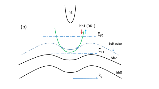
At some critical width the local maxima at of the sub-band will become lower than the bottom of the sub-band. It happens when
| (35) |
assuming that . At smaller values of it is possible to tune the Fermi level between and sub-bands. Then at there are no states at the Fermi level, and a sample constitutes a normal insulator, see Fig. 3(b). (To avoid confusion, we do not consider here the surface states which presumably exist on the side edges of the sample, and only mean the excitations which can be created in the ”bulk” of this quasi 3D sample). On the other hand, if the Fermi level is located again within the branch (above the edge of the bulk heavy-hole band and below the bottom of the sub-band), then only surface states are at the Fermi level, however under the condition indicated above their overlap is not exponentially small. Thus the situation shown in Fig. 3(b) corresponds rather to a normal insulator (semiconductor).
The general conclusion in the case of positive strain is that for the film widths within the usual experimental range of and for realistic strain values the overlap integral of the DK1 states belonging to the opposite boundaries is not small and spin conserving backscattering between them is not suppressed. As a result, it will destroy the robustness of the surface state.
VI.2 Negative (biaxially compressive in-plane) strain,
Let us consider biaxial, compressive in-plane strain (in accord with the definition we used in Ref. Khaetskii, it corresponds to the strain-induced energy ). Then for large enough sample without size-quantization effects we have a Dirac semi-metal (DSM) phase. We consider here the transition between the DSM phase and the quasi 3D (quantized) topological insulator phase (as it is called in the literature Coster ; Vail ) through the reduction of the layer width . We will argue that below some critical width the DSM transforms into an insulator which, strictly speaking, cannot be considered as topological for reasons similar to the ones described in the previous subsection. We consider the width in the interval
| (36) |
where is the width at which the upper branch of the Volkov-Pankratov states becomes inverted with the first quantized sub-band of the heavy holes , see Ref. Subashiev, . is the characteristic sample width at which the strain-induced energy is equal to the sum of the quantization energies of the light and heavy holes. (In the case of HgTe and for a realistic strain value corresponding to the length ). The left inequality in Eq. (36) means that the width is already large enough so that both branches of the Volkov-Pankratov states lie well below the energy of the point and we can describe the problem within the Luttinger model. The right inequality in Eq. (36) means that the width is small enough to “quench” the DSM state (i.e. the energy due to the size quantization is larger than the original overlap of the light and heavy-hole bands due to strain), and the transition to a new state has already happened. Our task is to understand the properties of this state. The physical pattern presented in recent publications (see, for example, Ref. Vail, ) is unclear, especially the nature of ”surface” and ”bulk” gaps discussed there.
We argue that the physics for this situation was described in Refs. (Dyak1, ,Subashiev, ). Though in both papers strain was assumed to be zero, this fact does not make a qualitative difference as far as we consider a situation when an original overlap of the light and heavy-hole bands is overcome by the size quantization. The only difference is that due to a ”compensation” of the negative strain by the quantized energies the energy difference between the bottoms of the and sub-bands can be small if one considers the situation close to the transition point (where ). Such a situation is assumed in Fig. 5, where several lowest sub-bands (closest to zero energy) are presented. Once again, due to the inversion, the branch increases with energy instead of decreasing and at large enough transforms into the DK1 surface state.
We claim that Fig. 5 corresponds to the situation presented in Fig. 2(c) in Ref. Vail, . (We note that Fig. 2(b) of Ref. Vail, demonstrates indeed that the width considered is already large enough, so that both branches of the Volkov-Pankratov states lie well below). The authors of Ref. Vail, named the distance between the bottoms of the and sub-bands as ”the bulk state band gap” and the distance between the bottoms of the (DK1) and sub-bands as ”the surface state band gap”. We see that these quantities actually have different physical meaning. We would say that the former quantity does not have any special physical meaning, but the latter should rather be named as ”the bulk gap” of this quasi 3D system, see also Ref. Dyak1, .
Assume now that the conditions of Eq. (36) are fulfilled, and, in addition, the Fermi level is within the (DK1) state, see Fig. 5. Then despite the fact that the Fermi level lies below the bottom of the first light-hole sub-band (), this DK1 state cannot be treated as a truly topological one since there is an appreciable overlap of the surface states wave functions located mostly at opposite boundaries (with the same spin orientations and opposite ). The reason for that is the fact that while keeping the Fermi level location below the bottom of the sub-band one cannot fulfill the condition , see the discussion in the previous subsection. As a result, an elastic impurity scattering which keeps the spin orientation but changes the sign of will destroy the robustness of the surface state.
The case of a relatively large negative strain when and one has the DSM regime is presented in Fig.4 by the green curve (for a HgTe quantum well). At the transition point the parameter . Thus the green curve corresponds to . If one takes to be much closer to , then the green curve will also be quite close to the blue one. Surely there is again a strong overlap of the DK1 surface states wave functions located mostly at opposite boundaries.
VII Conclusions
We have considered several problems in typical experimental situations related to topological surface states when a sample of the inverted-band material has a finite size and is subjected to strain. The main interest is to understand the physics of the series of transitions which happens at a given strain value with changing a sample width. In particular, we have considered analytically the DSM -3D quantized topological insulator transition. It is believed to occur in the case when for a large sample width one has a compressive in-plane strain which leads to an overlap of the light and heavy-hole bands (DSM regime). For this case our conclusion is actually opposite to those reached by the majority of the researchers. We have shown that near the transition point the surface state (DK1) cannot be treated as a truly topological one. At least this state cannot exhibit the topological properties in any transport experiments. The parameters of the problem near this point are such that an appreciable overlap of the surface states’ wave functions located at opposite boundaries occur. As a result, an elastic (and spin conserving) impurity scattering between the states located at opposite boundaries will destroy the robustness of the surface state.
While solving this problem we have obtained several other interesting and important results. For example, the effective boundary conditions for the solutions of the Kane model (with the contributions from the far bands) in the case of high barriers allows the use of this model to solve analytically various finite-size problems in the presence of strain for a realistic situation when heavy holes have finite masses. We hope that the results obtained can help in interpretation of current and future experimental data.
This work is supported by the Air Force Office of Scientific Research (FA9550-AFOSR-23RYCOR05). This research was performed while A. Khaetskii held an NRC Senior Research Associateship award at the Sensors Directorate, Air Force Research Laboratory. V.N.G. acknowledges financial support from the Spanish MCIN/AEI/10.13039/501100011033 through the projects PID2020-114252GB-I00 (SPIRIT) and TED2021-130292B-C42, as well as from the Basque Government through the grant IT-1591-22 and the IKUR strategy program. We thank S. Zollner for indicating to us Ref. Cardona, .
Appendix A Derivation of Eq. (33)
We derive here Eq. (33) and also obtain a shift of the central point of the V-P branches due to finite size effects in the limit of large width (). We rewrite Eq. (31) in the following form
| (37) |
and start with the case . Introducing , we look for the small correction , , where and is the solution of the zeroth order problem (), see Eq. (32). Assuming that the leading order of is proportional to , and keeping in the left hand side of Eq. (37) only the terms which contain the power of the exponent not higher than three (, we obtain
By squaring both sides of this equation (in this way we only need to keep the terms proportional to and ) we finally easily obtain
| (38) |
The first and the last terms determine the gap value, and the second one gives the shift of the central point of the V-P branches
| (39) |
Actually, under the condition we have used while deriving Eq. (39), the term in the brackets proportional to prevails. The shift is proportional to and is parametrically smaller than the gap value.
While deriving Eq. (33) we can neglect the shift value, as a result we can take the exponential function in the left hand side of Eq. (37) in the form ( is given by Eq. (32)). Then the problem reduces to a solution of the quadratic equation for , which gives the result Eq. (33), where we have neglected the exponentially small quantities everywhere except in the expression for .
Appendix B Exact equation for obtained within the Luttinger model for a finite-size sample in the presence of strain
We consider a film of the finite width and use zero boundary conditions on both surfaces. The exact equation that describes the critical value of where the quantized bulk-like state transforms into the surface DK1 branch reads
| (40) |
Note that in this Appendix the definition of is different from the one in the main text. Here these constants are ”full” Luttinger parameters, thus . Eq. (40) is obtained from the condition . The expression for presented above follows from the equation
| (41) |
using as identity. Note that Eq. (41) coincides with Eq. 22 of Ref. Khaetskii, and the quantity in Eq. (40) is nothing but the edge of the bulk heavy-hole band in the presence of strain. Therefore, at the point the heavy-hole components of the state transform from the form (localized near the center of the film) to the exponents which are localized more near the boundaries (DK1 state). It is possible to show that there is only one solution of Eq. (40) at , and for its solution coincides with the one obtained from the equations of Ref. Dyak1, . In the case the corresponding solution tends to the value given by Eq. (27) of Ref. Khaetskii, .
References
- (1) S. Groves and William Paul, PRL 11, 194 (1963).
- (2) S. Bloom and T. K. Bergstresser, Phys. Stat. Sol. 42, 191 (1970).
- (3) B. L. Gel’mont, V. I. Ivanov-Omskii, and I. M. Tsidil’kovskii, Sov. Phys. Usp. 19, 879 (1976).
- (4) M.I. Dyakonov, A.V. Khaetskii, JETP Lett. 33, 110 (1981).
- (5) B. A. Volkov, O. A. Pankratov, JETP Lett. 42, 178 (1985).
- (6) N. A. Cade, J. Phys. C: Solid State Phys. 18, 5135 (1985).
- (7) R. A. Suris, Sov. Phys. Semicond. 20, 1258 (1986).
- (8) O.A. Pankratov, S.V. Pakhomov and B.A. Volkov, Solid State Communications 61, 93 (1987).
- (9) Y. Ando, J. Phys. Soc. Japan 82, 102001 (2013).
- (10) M. Z. Hasan, C. L. Kane, Rev. Mod. Phys. 82, 3045 (2010).
- (11) X.-L. Qi, S.-C. Zhang, Rev. Mod. Phys. 83, 1057 (2011).
- (12) B. A. Bernevig, S.-C. Zhang, PRL 96, 106802 (2006).
- (13) C. L. Kane, E. J.Mele, PRL 95, 146802 (2005).
- (14) X. Dai, T.L. Hughes, X.-L, Qi, Z. Fang, and S.-C. Zhang, PRB 77, 125319 (2008).
- (15) Alexander Khaetskii, Vitaly Golovach, and Arnold Kiefer, PRB 105, 035305 (2022).
- (16) O. A. Pankratov, Sov. Phys. Usp. 61, 1116 (2018).
- (17) Y. Xia, D. Qian, D.Hsieh, L.Wray, A. Pal, H. Lin, A. Bansil, D. Grauer, Y. S. Hor, R. J. Cava, M. Z. Hasan, Nat. Phys. 5, 398 (2009).
- (18) D. Hsieh, Y. Xia, D. Qian, L. Wray, J. H. Dil, F. Meier, J. Osterwalder, L. Patthey, J. G. Checkelsky, N. P. Ong, A. V. Fedorov, H. Lin, A. Bansil, D. Grauer, Y. S. Hor, R. J. Cava, M. Z. Hasan, Nature 460, 1101 (2009).
- (19) C. Brüne, C. X. Liu, E. G. Novik, E. M. Hankiewicz, H. Buhmann, Y. L. Chen, X. L. Qi, Z. X. Shen, S.-C. Zhang, L. W. Molenkamp, PRL 106, 126803 (2011).
- (20) D. A. Kozlov, Z. D. Kvon, E. B. Olshanetsky, N. N. Mikhailov, S. A. Dvoretsky, D. Weiss, PRL 112, 196801 (2014).
- (21) J. G. Checkelsky, Y. S. Hor,M.-H. Liu, D.-X. Qu, R. J. Cava, N. P. Ong, PRL 103, 246601 (2009).
- (22) J. G. Analytis, J.-H. Chu, Y. Chen, F. Corredor, R. D. McDonald, Z. X. Shen, I. R. Fisher, PRB 81, 205407 (2010).
- (23) Z. Ren, A. A. Taskin, S. Sasaki, K. Segawa, Y. Ando, PRB 84, 165311 (2011).
- (24) B. Xia, P. Ren, A. Sulaev, P. Liu, S.-Q. Shen, L. Wang, PRB 87, 085442 ( 2013).
- (25) Y. Pan, D. Wu, J. R. Angevaare, H. Luigjes, E. Frantzeskakis, N. de Jong, E. vanHeumen, T. V. Bay, B. Zwartsenberg, Y. K. Huang, New J. Phys. 16, 123035 (2014).
- (26) Yo. Ohtsubo, P. Le Fevre, Francois Bertran, and A. Taleb-Ibrahmi, PRL 111, 216401 (2013).
- (27) G. J. de Coster, P. A. Folkes, P. J. Taylor, and O. A. Vail, PRB 98, 115153 (2018).
- (28) Le Duc Anh, Kengo Takase, Takahiro Chiba, Yohei Kota, Kosuke Takiguchi, and Masaaki Tanaka, Adv. Mater. 33, 2104645 (2021).
- (29) L.G. Gerchikov, and A.V. Subashiev, Phys. Stat. Sol. (b) 160, 443 (1990).
- (30) G. Bir and G.E. Pikus, Symmetry and Strain-induced Effects in Semiconductors (John-Wiley and Sons, Chichester, 1974).
- (31) G. Bastard, Wave Mechanics Applied to Semiconductor Heterostructures (Halstead Press, New York, 1988).
- (32) M. I. Dyakonov, A.V. Khaetskii, Sov. Phys. JETP 55, 917 (1982).
- (33) A. Engel, private communication.
- (34) M. Cardona, N. Christensen, PRB 35, 6182 (1987).
- (35) Chang Liu, Guang Bian, Tay-Rong Chang, Kedong Wang, Su-Yang Xu, Ilya Belopolski, Irek Miotkowski, Helin Cao, Koji Miyamoto, Chaoqiang Xu, Christian E. Matt, Thorsten Schmitt, Nasser Alidoust, Madhab Neupane, Horng-Tay Jeng, Hsin Lin, Arun Bansil, Vladimir N. Strocov, Mark Bissen, Alexei V. Fedorov, Xudong Xiao, Taichi Okuda, Yong P. Chen, and M. Zahid Hasan, PRB 92, 115436 (2015).
- (36) Z. Lu, G. L. Chiarotti, S. Scandolo and E. Tosatti, PRB 58, 13698 (1998).
- (37) L. Seixas, D. West, A. Fazzio and S.B. Zhang, Nature Communications (2015); doi: 10.1038/ncomms8630
- (38) Anna Pertsova, Peter Johnson, Daniel P. Arovas, and Alexander V. Balatsky, Phys. Rev. Research 3, 033001 (2021).
- (39) T. Dietl, PRB 107, 085421 (2023).
- (40) Strictly speaking, the overlap integral is a 2x2 matrix, because of the spin degeneracy in the symmetric quantum well. However, that matrix can be reduced to a scalar due to the time-reversal symmetry of the Hamiltonian after a suitable choice of the basis.
- (41) Owen Vail, Alex Chang, Sean Harrington, Patrick Folkes, Patrick Taylor, Barbara Nichols, Chris Palmstrøm, George de Coster, Journal of Electronic Materials (2021); doi.org/10.1007/s11664-021-09126-w