Modeling of Plasmonic and Polaritonic Effects in Photocurrent Nanoscopy
Abstract
We present a basic framework for modeling collective mode effects in photocurrent measurements performed on two-dimensional materials using nano-optical scanned probes. We consider photothermal, photovoltaic, and bolometric contributions to the photocurrent. We show that any one of these can dominate depending on frequency, temperature, applied bias, and sample geometry. Our model is able to account for periodic spatial oscillations (fringes) of the photocurrent observed near sample edges or inhomogeneities. For the case of a non-absorbing substrate, we find a direct relation between the spectra measured by the photocurrent nanoscopy and its parental scanning technique, near-field optical microscopy.
I Introduction
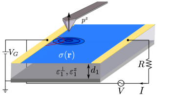
Scanning photocurrent microscopy is traditionally performed using a focused light beam [1, 2, 3, 4]. In a modern variant of this technique, the focusing of incident light is achieved instead by a sharp metal tip, as illustrated schematically in Fig. 1. Such a tip acts as an optical antenna that couples a locally enhanced near-field to free-space radiation. In experiment, the tip is scanned and the dc photocurrent current generated in the sample is measured as a function of the tip position using electric contacts positioned somewhere on the sample periphery. Below we refer to this technique as scanning near-field photocurrent microscopy or photocurrent nanoscopy. The instrumentation involved in such measurements can also be utilized to perform scattering-type scanning near-field optical microscopy (s-SNOM). In s-SNOM one detects light scattered by the tip instead of the photocurrent. In practice, s-SNOM and photocurrent nanoscopy are performed together, providing complementary information about the system. This combination of techniques has been successfully applied to probe graphene and other two-dimensional (2D) materials [5, 6, 7, 8, 9] demonstrating spatial resolution of , which is orders of magnitude better than the diffraction-limited traditional approach.
Recent photocurrent nanoscopy experiments revealed distinctive spectral resonances and periodic interference patterns occurring near sample edges and inhomogeneities [6, 7, 8, 9]. These features have been attributed to collective modes, plasmon- and phonon-polaritons, excited in graphene and underlying 2D substrate materials. In this paper, we aim to formulate a theoretical model for such collective mode effects.
Whereas modeling of s-SNOM has been actively pursued in the past decade [10, 11, 12, 13], photocurrent nanoscopy has received less attention. Theoretical analysis of the latter is more effortful because in addition to the electromagnetic tip-sample coupling, one also has to account for multiple possible mechanisms of the DC photocurrent generation. We focus on the case where the photocurrent scales linearly with the incident light intensity, i.e., as a second power of the in-plane AC electric field . Assuming the system contains only inversion-symmetric materials, such a second-order nonlinear effect can arise if the inversion symmetry is violated by boundary conditions, structural defects, or externally applied fields. For example, nonvanishing photocurrent can exist if the carrier density in the scanned region is nonuniform. Photocurrent can also be generated if the magnitude or the phase of is spatially dependent (the latter corresponds to a nonzero in-plane momentum) [14]. If there exists a DC electric field in the system, the photocurrent can include terms that scale as , which we also consider in our calculations. Altogether we examine three mechanisms of photocurrent generation: bolometric (BM), photothermal (PT), and photovoltaic (PV). The relative importance of the BM, PT, and PV effects depends on a system. In common bulk semiconductors, the Joule heating of charge carriers is suppressed by an efficient cooling by optical phonons [16]. The resultant PT current is small and the photocurrent is mostly due to the PV effect. In graphene, the linear quasiparticle dispersion combined with the high optical phonon frequency inhibits electron cooling, which enhances the PT contribution [17, 18]. Experiments performed on graphene - junctions have demonstrated that in the absence of a bias, , the PT effect is typically the dominant photocurrent mechanism [19]. However, the BM current quickly becomes the largest contribution as the bias is increased from zero [20].
As we show in the remainder of this paper, collective mode effects in photocurrent, which is the main target of our investigation, can manifest themselves via all these three mechanisms. In Sec. II, we introduce basic definitions and relations concerning the BM, PT, and PV effects. In Sec. III, we present illustrative examples how collective modes — plasmons and polaritons — can generate characteristic spatial patterns detectable in photocurrent nanoscopy. In Sec. IV we study the collective mode signatures in the frequency dependence of the PT photocurrent. We present main equations of our model in Sec. V. Further technical details are given in the Appendix.
II Definitions of photovoltages, currents, and conductivities
The model system we study is shown schematically in Fig. 1. The measured quantity is the total current given by
| (1) |
where is the bias voltage applied between the contacts, is the photovoltage (discussed below), is the sample resistance in the dark, and is any additional resistance in series with , e.g., the contact resistance. Assuming remains constant under illumination, the photocurrent is proportional to , which is in turn proportional to the local photoinduced electromotive force (EMF) . If , the EMF in the dark
| (2) |
and the linear-response DC conductivity were all uniform, and the sample were infinite, the two EMFs would be simply additive. (Here is the equilibrium distribution of the chemical potential and is the electron charge.) The photoinduced EMF would drive an extra uniform current
| (3) |
In the practice of photocurrent nanoscopy, is nonuniform, the sample is of finite size and may have an irregular shape. In such a case Eq. (3) serves as a formal definition of ; however, the actual current density is different because the total EMF must readjust itself to ensure current conservation in the steady state. Nevertheless, the relation between and (or equivalently, ) can be conveniently expressed using the Shockley-Ramo theorem (see, e.g., Ref. [15]):
| (4) |
Here the repeated index is meant to be the summed over,
| (5) |
is the current density in the dark, and is the total dark current. The auxiliary vector field , which has the units of inverse length in 2D, encodes all the geometric properties of the sample and contacts and obeys the normalization relation
| (6) |
As mentioned in Sec. I, we consider three contributions to the photoinduced EMF . The first one is due to the photothermal (PT) effect:
| (7) |
where is the tensor of Seebeck coefficients (same as the thermopower tensor). The electron temperature that enters this equation differs from the equilibrium ambient temperature because of AC Joule heating. We assume that the relation between and the heating power is linear, so that the gradient of is quadratic in the incident AC field. Therefore, it is possible to express the PT EMF and the corresponding current density in terms of a suitable rank-three tensor :
| (8) |
Since the temperature distribution is also affected by the sample geometry and mechanisms of heat dissipation, this tensor may depend on position and various extrinsic factors. The relation between , , and other material properties will be further elaborated on in Sec. V.
The second contribution we include is due to the bolometric (BM) correction to the DC conductivity . The corresponding corrections to the EMF and the current density satisfy the equation
| (9) |
The BM coefficient is briefly discussed in Sec. III. As with the PT photocurrent, it is in principle possible to rewrite Eq. (9) in terms of a certain rank-three tensor but we will not do so.
Lastly, we consider the photovoltaic (PV) current:
| (10) |
(It is also referred to as the photogalvanic current in some literature.) In Eq. (10), we split the PV response into the coherent part (the first term), due to the AC electric field, and the incoherent part (the second term), caused by the change of the chemical potential due to the heating and/or the photoexcited carrier density . Similar to the points made above about the PT and BM currents, the sum of these two parts can also be written using a certain tensor :
| (11) |
In turn, the full second-order conductivity tensor is the sum
| (12) |
Having it defined in the present work allows us make a connection with prior literature where such a tensor has been studied [31]. We discuss this in Sec. V.
III Photocurrent signatures of collective modes in imaging: three illustrative examples
III.1 Hot spots due to polaritonic rays
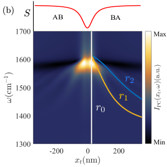
Optical phonon modes of 2D heterostructures are examples of collective excitations which may generate uncommon effects detectable by photocurrent nanoscopy. As one illustration, we consider a model system consisting of twisted bilayer graphene (TBG) deposited on a thin slab of hBN, Fig. 1. In our previous work [21] the photocurrent in such a system has been experimentally found to exhibit characteristic spatial variations near the domain walls of TBG. These domain walls (also known as AB-BA boundaries or “solitons”) form naturally in TBG if its twist angle is small enough. Below we discuss modeling of these experiments and our theoretical predictions for observable collective mode signatures. We give some additional background necessary to understand these results but otherwise delay all the derivations until Sec. V.
An interesting property of hBN is its optical hyperbolicity: the in- and out-of-plane permittivities of this material are of opposite sign in certain frequency bands, known as Reststrahlen (RS) bands, such as . The optical hyperbolicity enables propagation of so-called hyperbolic phonon-polaritons inside the slab [22, 23]. A localized source, such as an s-SNOM tip, typically excites several of such polariton modes simultaneously, which produces a spatial beats pattern with the period given by the formula
| (13) |
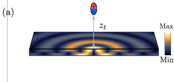
Furthermore, inside the hBN slab, the electric field is strongly concentrated along certain zigzag trajectories, which we refer to as polaritonic rays, Fig. 2(a).
The results presented below are obtained using the following additional assumptions. First, we approximate the scanned probe as a point-like dipole located at a distance above the sample as shown in Fig. 2(a). Such an approximation, referred to as the “point dipole model” [24, 10], is commonly used in s-SNOM modeling. Note that is really an adjustable parameter rather than the physical tip-sample distance. Usually it is chosen to be of the order of the curvature radius of the probe.
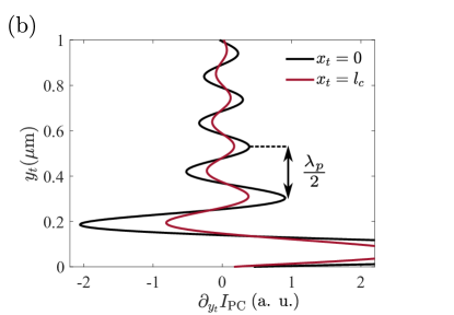
Second, we assume that the photocurrent is dominated by the PT effect that arises due to the local mimimum of the thermopower at the domain wall, Fig. 2(b). Finally, we assume that the domain wall is infinitely long, so that the sample and therefore the photocurrent signal are translationally invariant in the longitudinal direction.
The results obtained within this model are shown in the lower part of Fig. 2(b). At frequencies outside its RS band, the hBN layer is not hyperbolic and only two peaks of photocurrent signal as a function of tip position are observed. They appear when is approximately equal to the tip-sample separation . The qualitative explanation is that at such the Joule heating at the domain wall is the largest, which generates the strongest photoresponse. Indeed, the Joule heating is proportional to the square of the in-plane electric field produced by the dipole. It vanishes directly below the dipole [which is the case in general, including the hyperbolic regime, Fig. 2(a)] and is maximal at the lateral distance .
At frequencies inside the RS band, our calculation predicts additional peaks of photocurrent as a function of , which we have referred to as the “hot spots” in the past. For a given , these hot spots are separated by intervals approximately equal to . More precisely, they appear when the tip position matches the radii
| (14) |
of “hot rings” created by the polaritonic rays launched by the tip [Fig. 2(a)]. If is much larger than the tip-sample distance , our calculation predicts multiple rings to be well resolved. At small , the rings overlap and only weak oscillations with the period remain. Only the first pair of hot spots has been observed in the experiment [25]. We expect that using cleaner samples and higher resolution probes may reveal additional ones.
III.2 Interference fringes due to the plasmons: PT and BM effects
Plasmons are another example of collective modes that have been imaged by both s-SNOM [26, 23, 27, 6] and photocurrent nanoscopy [28, 25]. Such an imaging is typically done near sample boundaries that reflect plasmons launched by the scanned probe. Near a sample edge, the incident and reflected waves interfere, resulting in a standing-wave pattern (or “fringes”) with spatial period where is the plasmon wavelength and is the plasmon momentum. Following the structure of Sec. III.1, below we present our modeling results for this effect but defer their derivation until Sec. V. We begin the cases where the photocurrent is generated by the PT and BM mechanisms. An example of PV plasmonic fringes is presented later in Sec. III.3.
III.2.1 Edge-reflected plasmons near a - junction
Rigorous calculation of the plasmon reflection from the edge is computationally intensive [26]. However, there is a simple model where the reflection from the edge () is approximated by the method of images. For the tip located at , we place an “image” tip at . The corresponding in-plane electric field is the superposition of the source and image terms:
| (15) |
where is the in-plane field produced by the tip in an infinite uniform sample. This approximation is reasonably accurate. Its main deficiency concerns the position and the amplitude of the very first fringe.
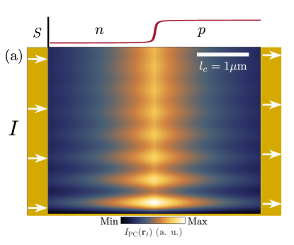
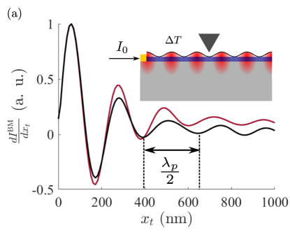
As an illustrative example of how plasmons show up in the PT photocurrent signal, we consider the case where the sample contains a - junction along the -axis, i.e., , which is normal to the sample edge at . This geometry models the case studied experimentally [28]. We approximate the thermopower profile by a step-like function of coordinate . We also assume is uniform, thereby neglecting the suppression of in a neighborhood of the junction. To obtain the temperature distribution, we again use the method of images approximation:
| (16) |
where is the temperature profile in an infinite uniform sample, the top (bottom) sign corresponds to a boundary with vacuum (metal), and we set the ambient temperature to zero, for simplicity. (The value of does not affect the result for the photocurrent.)
The spatial distribution of the photocurrent signal computed within this model is shown in Fig. 3. The photocurrent exhibits plasmonic fringes as a function of the tip coordinate due to the interference of the tip-launched modes with their reflections off the edge, as observed in the experiment [28, 29]. It can be seen from Fig. 3(a) that appreciable photocurrent is generated only when the lateral tip position is close enough to the - junction, . The cooling length is defined in Sec. V.4. It was chosen to be in this calculation. The fringe periodicity does not depend on ; however, the fringe amplitude decreases with , see Fig. 3(b). The decay law of the excess temperature (and so, photocurrent) as a function of distance is discussed in more detail in Sec. V.4.
III.2.2 Biased sample
If the sample carries a DC current already in the absence of light, another possible mechanism of photocurrent plasmonic fringes is the BM effect. The scanned probe locally modifies the temperature distribution, which causes a local variation in the conductivity. The size of the BM effect is proportional to the derivative , which depends on details of electron scattering, see Sec. V. The total BM photocurrent in a rectangular sample of size is
| (17) |
The results of our calculations done using this equation are plotted in Fig. 4(a). They exhibit the now familiar fringes near the contacts. It appears that there are many similarities between the spatial features observable in PT and BM photocurrent. In fact, in Eq. (17) depends on the tip position in exactly the same way as the PT photocurrent in a sample with a linearly varying thermopower .
In principle, photocurrent in a biased sample can be also generated through the PT because the source-drain bias causes self-gating, i.e., the carrier density change across the sample, with being the capacitance. To show that the BM should normally be more important than the PT, we compare the coefficients of Eqs. (17) and (80). Using Eq. (51) for the thermopower and a rough estimate , we find
| (18) |
Indeed, experiments show that the BM contribution typically dominates over the PT one [20].
III.3 Interference fringes due to the plasmons: coherent PV effect
The remaining contribution to the photocurrent introduced in Sec. I is the PV term. The PV effect is a complicated phenomenon that depends on many microscopic details of the system. Therefore, as our final example, we study the appearance of plasmonic fringes within a simple representative model. We assume again that our graphene sample is uniformly doped, and has the shape of a rectangle with contacts at and , as in Fig. 1. In the absence of an applied bias voltage , the chemical potential and the thermopower are also uniform, . Hence, the BM, PT, and the thermal PV photocurrents all vanish. What remains is the coherent PV current, which is given by Eq. (10). A particularly simple result is obtained in the hydrodynamic regime, where the largest contribution to in the limit is given by the ponderomotive force [30, 31]:
| (19) |
Therefore, the current is proportional to the difference of field intensities at the contacts. If the field on the contact is the sum of the external field and the field created by the tip, the PV current is
| (20) |
Here, is a phase shift which contains the reflection coefficient from the contact, as well as any phase shift depending on the properties of the tip. Equation (20) is plotted in Fig. 4(b). When the tip is located halfway between the source and drain, the photocurrent vanishes, since then the tip-sample system is inversion-symmetric. The spatial period of the fringes is , which is twice the period of the standing waves observed in the PT, BM, and in s-SNOM. This qualitative difference is a result of the interference between the external and the tip-launched field, in contrast the the interference between the launched and reflected waves in PT or s-SNOM, see Table 1. More complicated models would be necessary to accurately model plasmon reflection from the contact [32] or the effect of probe shape and composition [12] on the photocurrent.
| Effect type | Photocurrent scaling | Fringe period |
|---|---|---|
| PT | ||
| PV | ||
| BM |
IV Photocurrent spectra versus s-SNOM spectra
In the preceeding Section we dealt with the tip-position dependence of the photocurrent. Collective mode effects have also been observed in the frequency dependence of both photocurrent nanoscopy [34] and the s-SNOM measurements [33]. It is interesting to ask whether the frequency dependencies obtained through these two techniques can be related to one another. Below we discuss one case where such a mathematical relation can be established.
The s-SNOM signal is a measure of the dipole moment induced on the probe by the sample [24]. For a long and thin probe oriented normal to the surface, this signal is proportional to the out-of-plane component of the probe dipole moment :
| (21) |
with some frequency-independent constant of proportionality . The total power dissipated by the probe driven by an external field can also be expressed through its dipole moment:
| (22) |
PT, BM, and PVT photocurrents depend on the excess temperature, which is proportional to the Joule heating . In fact, we can show that for the setup examined in Sec. III.1, i.e., the tip near a domain wall in TBG, the PT photocurrent is proportional to the total Joule heating:
| (23) |
see Eqs. (32), (73), and (76). As with , constant has no frequency dependence.
Within the quasistatic approximation, radiation losses are negligible, so the dissipation is dominated by losses in the sample. Furthermore, if dielectric losses are negligible compared to the Joule heating, by conservation of energy. The equality of losses in the sample and the dissipation by the polarizable probe provides an elegant connection between the s-SNOM signal and photocurrent :
| (24) |
Although we worked within the simple point-dipole approximation in Sec. III, this correspondence only requires Eq. (21) to be applicable, allowing more complicated models developed for s-SNOM modeling [10, 11, 12] to be extended to near-field photocurrent techniques.
Finite dielectric losses lead to deviations from Eq. (21) and so Eq. (24). A rough validity condition for Eq. (21) can be obtained from the point dipole model of the tip [10]. It is given by
| (25) |
where is the radius of curvature of the tip and is the permittivity of the substrate.
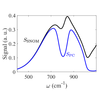
To illustrate how well Eq. (21) works in a concrete example, we consider a system where graphene layer is deposited on SiO2 substrate near a - junction. The modeled s-SNOM signal, PT photocurrent, and their ratio are illustrated in Fig. 5. The peak in the signal due to the graphene plasmon, observed both in s-SNOM [33] and photocurrent [35], is present in both measurements. This sample satisfies the low-loss condition Eq. (25) away from the phonon resonances of SiO2 that occur near and [36]. (The latter is not visible in Fig. 5.)
The above discussion suggests that a photocurrent signal relates more directly to the properties of the 2D conductor and less to those of the substrate, potentially making photocurrent measurements more suitable for extracting properties of conducting layers embedded in complicated heterostructures.
V Model
V.1 Optical response of a layered medium
In this Section we go over computational aspects of our modeling. We start with presenting the set of equations we have used to compute the optical response of the systems discussed in the previous Section. All those model systems are layered heterostructures of the type depicted in Fig. 1. We number the layers sequentially top to bottom. The vacuum half-space above the sample is layer . The bottom substrate, which we also treat as semi-infinite, is layer . We allow for a uniaxial anisotropy of the layer materials, such that the in- and out- of plane permittivities of layer may be unequal. Additionally, if any of the constituent materials can be considered 2D, we do not assign it an index. Instead, we model it as a zero-thickness sheet of ac conductivity at the interface of layers and . (If no such 2D material is present at that interface, then .)
In general, the optical response of the system is determined by the reflection coefficients of polarizations or . However, in the near-field limit, only the -polarization reflection coefficient is important. This quantity can be computed from the following recursion formula [37]:
| (26) | ||||
| (27) |
where is the in-plane momentum, is the thickness of layer , and is the reflection coefficient of the interface between layers and :
| (28) |
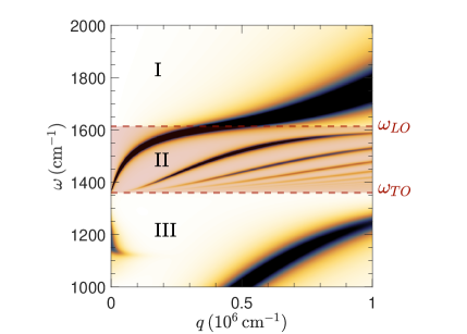
The recursion starts with for which , and continues to progressively smaller . The reflection coefficient of the entire system is given by . For real , the reflection coefficient has an absolute value smaller than unity. Away from this radiative zone, function may have poles at some complex that have relatively small imaginary parts. Such poles define the dispersion of the propagating collective modes of the system whose effect on photocurrent we want to study.
An illustrative example of function is shown in Fig. 6. It is computed for a heterostucture consisting of a doped monolayer graphene placed on a -thick hBN crystal, which is in turn placed on a bulk SiO2 substrate. At low frequencies (Region I) the dispersion of this system contains a single branch, which is basically the plasmon mode of graphene. However, there is also a weak feature present near , which is due to the interface phonon of hBN and SiO2. In a range of intermediate frequencies (Region II) where hBN acts as a hyperbolic material, with , there are multiple dispersion branches. These are known as hyperbolic phonon polaritons. More precisely, these modes result from hybridization of the graphene plasmon with phonon polaritons of hBN, and so they should be referred to as the hyperbolic plasmon phonon polaritons. At high frequencies there is only a single plasmon branch.
Our goal in this paper is to understand the effect of these collective modes on photocurrent measured by scanned probes.
Let us now discuss the electric field produced by such a probe. Computing this field from a realistic model can be quite laborious. Instead, as common in the s-SNOM literature [24, 10, 33, 12], we model the tip of the probe by a polarizable dipole of amplitude positioned a distance from the sample. If , the field produced by the tip can be computed within the quasi-static approximation. The scalar potential produced by the tip in the half-space above the sample is the superposition of the bare and the reflected dipole potentials:
| (29) | |||
| (30) |
In turn, the in-plane field and the local Joule heating in the 2D layer where the photocurrent is produced are given by
| (31) | |||
| (32) |
where is the Bessel function of the first kind of order . Here we assume that the AC conductivity of the 2D layer varies slowly on the scale of .
V.2 Plasmonic response of the 2D layer
The continuity equation for a time-harmonic perturbation of frequency to the charge density is
| (33) |
The collective excitations of the system, e.g., plasmon-phonon modes illustrated by Fig. 6 invariably involve oscillations of and . We can center our attention on the 2D layer and consider the rest of the system an environment. It is then possible to take a point of view that all collective excitations are 2D plasmons renormalized by the environment. Within this approach, the derivation of the mode spectra goes as follows. First, we find the reflection coefficient of the system without the conducting 2D layer on top, by the procedure explained above. All the charges above the sample are now considered the sources of an external potential , which is computed similar to Eq. (29) except with replaced by . The total in-plane potential is the sum of this and the potential induced by the 2D layer’s own charge :
| (34) |
(Here we again assume the quasi-static limit .) Combining these equations, we arrive at
| (35) |
where the function
| (36) |
has the physical meaning of the effective 2D permittivity of the conducting layer. The relation between , , and is
| (37) |
The imaginary part of characterizes the losses of the system. For a general multilayer structure, the low-loss condition can be expressed as
| (38) |
at , where is the radius of curvature of the near-field probe, see Eqs. (26) and (34). For a graphene layer at the interface of two semi-infinite media, one recovers Eq. (25). The sought mode dispersions are the poles of or equivalently, the zeros of . At a given , these zeros occur at momenta that solve the equation
| (39) |
In general, such are complex and the corresponding collective modes are well defined (underdamped) only if . Within the Drude model [Eq. (48)], , so the necessary condition for underdamped plasmons to exist is .
The potential of a plasma wave launched by a local source (such as an s-SNOM tip) is given by
| (40) | ||||
| (41) |
where is the Hankel function of the first kind. For an arbitrary sample-gate separation , Eq. (40) remains universally valid in the range of distances but Eq. (41) may be modified. If such distances play the dominant role in the photocurrent response and the absolute magnitude of this response is not of primary interest, then it is permissible to use the simple equations (40)–(41) to find the potential , see Sec. III.3.
If the 2D layer resides on a hyperbolic film of thickness , e.g., if , , then is given by
| (42) |
In this case, Eq. (39) has an infinite number of roots, each representing a different plasmon-phonon eigenmode, see region II in Fig. 6. The solutions are separated by the constant value
| (43) |
We can use Eq. (42) to find the in-plane components of the electric field:
| (44) |
where
| (45) |
Since in the hyperbolic regime, the largest term in the series is the term. These fields have maxima at the concentric rings of radius , given by Eq. (14). If the slab were made of a non-hyperbolic material, then would be imaginary and the only real roots of Eq. (14) would be . For instance, in an isotropic material and the rings are absent. The effect of for large is negligible in this case, since the image dipoles become progressively further from the origin.
V.3 Second-order response of a 2D layer
If the electric field is not too strong, the response of the system can be studied by expanding all quantities of interest in power series of the electric field. For example, the current density has the expansion The second term, quadratic in , can be expressed in terms of the second-order nonlinear conductivity entering Eq. (12). For the DC photocurrent generated by a monochomatic field of frequency , the parameter choice is appropriate, such that
| (46) |
where
| (47) |
The functional form of is highly system-dependent. One particular case attracting much interest recently is where the electrons behave collectively, as a fluid [38]. This regime is realized when the momentum-conserving electron-electron scattering rate exceeds the momentum relaxation rate . In this hydrodynamic regime, the derivation of the second-order non-linear response simplifies greatly. We summarize it in Appendix A.
The first-order ac conductivity is given by the Drude formula
| (48) |
For the second-order current, we find the following combination of terms:
| (49) |
The first term is the PT current
| (50) |
Comparing with Eq. (7), we see that the thermopower coefficient is equal to the entropy per unit charge
| (51) |
The last equation is Mott’s formula for a degenerate Fermi gas with a constant scattering rate . The next term in Eq. (49) is the thermal PV current
| (52) |
Lastly, the third term in Eq. (49) is what we previously called the coherent part of the PV current. After a lengthy but straightforward derivation, one finds (see, e.g., [31])
| (53) |
This expression is well known in plasma physics where it is attributed to the ponderomotive force [30]. For , the largest term is the first term in the curly brackets, which is Eq. (19).
In the regime of our primary interest , the results for the PV and PT parts of simplify to
| (54) | ||||
| (55) | ||||
| (56) |
Under the assumption made earlier, the PT component is the dominant one. Note that the extra factor of in the first term of Eq. (55) compared to Eq. (53) appears when we make the transition from the real to the Fourier space. In addition, the derivative entering the second term in Eq. (55) is very small for a degenerate 2D Fermi liquid .
In the scenario considered in Sec. III.3, only the PVC contributes to the photocurrent. Assuming , the current through a resistor can be obtained from integrating Eq. (53):
| (57) |
where is the resistance of the sample. This integral immediately simplifies to
| (58) |
which indicates that is determined solely by the electric field at the contacts. In Eq. (58) we took into account that the contacts are equipotential so that must vanish. The tip-dependent contribution to the field comes from the interference between the tip-generated and external fields:
| (59) |
which is Eq. (20) with .
V.4 Thermal response
.
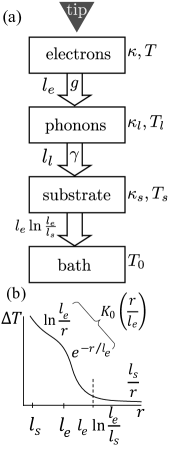
The energy relaxation of electrons involves their interaction with multiple degrees of freedom such as the phonons of the 2D layer and the substrate. In this section, we consider a model where we assign separate temperatures to these two subsystems. This can be a reasonable approximation if far-from-equilibrium effects (phonon wind, phonon amplification, hot electrons, etc.) can be neglected [39, 40, 41]. We introduce the electron-phonon coupling constant and the inverse of the Kapitza resistance of the graphene-substrate interface and write the following three-temperature heat transfer equations:
| (60) | |||
| (61) | |||
| (62) |
The Joule heating power produced by the scanned probe acts as a localized heat source, as shown in Fig. 7(a). The electronic and lattice thermal conductivities, and , define three characteristic lengths
| (63) | ||||
| (64) | ||||
| (65) |
Depending on their values relative to each other and the distance from the source, qualitatively different scaling laws for the excess electron temperature emerge, as discussed below. For defineness, we consider the case where electron cooling into the substrate heat sink is efficiently mediated by graphene phonons: and . For graphene on SiO2, these assumptions can be justified using the following parameter estimates [42, 43, 44]
| (66) | ||||
| (67) |
In Eq. (66) we employ the commonly reported “bulk” thermal conductivity , which is calculated by modeling graphene as a thin film of thickness . The phonon mean-free path corresponding to the chosen value is [43] . These parameter values yield the estimate , which is substantially shorter than the typical values of the cooling length reported for encapsulated graphene systems. As discussed below, this is due to the fact that the limiting step in the cooling process is the energy exchange between electrons and phonons of graphene.
To get the remaining parameters in Eqs. (63)–(65), we first use the Widemann-Franz law
| (68) |
where we took and , corresponding to the transport mean-free path of at electron density . Second, to estimate and , we assume that is higher than the Bloch-Grüneisen temperature
| (69) |
In this regime the electron cooling power due to scattering by acoustic phonons is given by [17, 45]
| (70) |
where is the sound velocity, is the coupling constant for the strain-induced effective gauge potential, is the graphene mass density per unit area, is the electron specific heat per unit area. In the second equation in Eq. (70) we introduced the momentum relaxation time due to electron-phonon scattering, which enables us to relate the length scales and . Indeed, from Eqs. (68) and (70), we obtain
| (71) |
Assuming that the DC conductivity is dominated by electron-phonon scattering, so that , we estimate at . The length is much larger than because at the electron-phonon scattering is quasi-elastic. The net cooling length is determined by the larger of and . In the present case,
| (72) |
Finally, we find for an SiO2 substrate, which is significantly shorter than and . The electronic cooling length is determined mostly by the doping of the graphene and the electron-phonon coupling, whereas also depends on the interfacial resistance between the graphene and the substrate. We expect the effect of the substrate to have the largest impact on the thermal transport properties of the system through the length ; for a conducting substrate like gold, this length could exceed . In this work, we consider only the case . For such interrelations among these characteristic length scales, the behavior of the excess electron temperature generated by a local heat source is sketched in Fig. 7(b). In particular, at short distances, is described by the equation
| (73) |
where is the MacDonald function. This temperature profile has a narrow region of exponential decay for . At large distances, however, we find the inverse-distance law
| (74) |
Our derivation of these formulas is presented in Appendix B.
Having defined a model for the temperature, we can now extract the parameter in Eq. (17) experimentally by measuring non-Ohmic corrections to the current as a function of in the absence of light. Using our model for heat transfer Eq. (73), the corresponding correction is of the form
| (75) |
The cubic nonlinearity predicted by this formula implies that when is periodically modulated at some small frequency , the current contains the third harmonic of this frequency. Measuring this -signal can then be used to obtain the bolometric coefficient .
To generate a net PT photocurrent, a spatially inhomogeneous thermopower is required. We limit ourselves to one-dimensional (1D) inhomogeneities and consider three examples: having a sharp peak, exhibiting a step-like change, and being a linear function of a spatial coordinate . Such profiles of can originate from a stacking defect (domain wall) in a multilayered material, a doping inhomogeneity (e.g, a - junction in graphene), or self-gating in a voltage-biased device. If the dc conductivity is a slowly varying function of position, the local thermoelectric coefficient can be estimated from Eq. (51). If the source and drain contacts are long conducting strips (Fig. 1) located at and , the function [Eq. (4)] does not have a -component, and the PT photocurrent can be written in the form
| (76) |
where is the line-integrated excess temperature
| (77) |
Assuming the tip is far from the sample edges or contacts, we can assume the translationally invariant form .
Suppose now that function has a sharp dip of characteristic depth and width that we can approximate by . This is reasonable for, e.g., domain wall (DW) defect whose width is typically much smaller than the cooling length. Substituting this into the equations above, we obtain
| (78) |
This expression was used to obtain Fig. 2(b). Next, for the thermopower profile characteristic of a - junction, we find
| (79) |
The plot in Fig. 3(a) was obtained using the equation above, together with Eqs. (32), (40), and Eq. (73). Finally, for a linear profile, , we get
| (80) |
which has the same dependence as Eq. (17). In deriving all these results we assumed, for simplicity, that the temperature of the contacts and the adjacent graphene regions is maintained at the ambient value , and so the possible difference in the thermopower of the contacts and graphene does not contribute to .
VI Conclusion
In this paper, we demonstrated applications of several minimal models for scanning near-field photocurrent measurements on graphene-based heterostructures where effects of plasmon- and phonon-polaritons may be important. Such collective modes can generate interference patterns near sample edges and other inhomogeneities and exhibit distinctive spectral resonances. Our models reproduce these interference patterns and elucidate the role of the thermal properties of the heterostructure on the collected signal. We also studied a coherent photovoltaic contribution to the photocurrent induced by the scanned probe. Additionally, we derived a simple relation connecting the frequency dependence of these measurements to that of the parent technique of s-SNOM for the case where dielectric losses in the substrate are negligible.
In this work, we focused mostly on effects that are quadratic in applied electric field. On the other hand, a non-perturbative regime of strong applied bias [46] may be an interesting direction for future investigations. The effects of band structure and especially geometrical phases [47, 48] on photocurrent also warrant study in the novel context of near-field measurements. We hope that our modeling of collective mode phenomena in the photocurrent response will be useful in these and other future studies.
Acknowledgements.
We thank S. S. Sunku, D. Halbertal, Z. Sun, and Y. Dong for discussions that inspired this work.References
- Kallmann et al. [1960] H. Kallmann, B. Kramer, J. Shain, and G. M. Spruch, Photovoltaic effects in CdS crystals, Physical Review 117, 1482 (1960).
- Güttler and Queisser [1970] G. Güttler and H. Queisser, Impurity photovoltaic effect in silicon, Energy Conversion 10, 51 (1970).
- Marek [1984] J. Marek, Light-beam-induced current characterization of grain boundaries, Journal of Applied Physics 55, 318 (1984).
- Graham and Yu [2013] R. Graham and D. Yu, Scanning photocurrent microscopy in semiconductor nanostructures, Modern Physics Letters B 27, 1330018 (2013).
- Basov et al. [2014] D. Basov, M. Fogler, A. Lanzara, F. Wang, and Y. Zhang, Colloquium: Graphene spectroscopy, Reviews of Modern Physics 86, 959 (2014).
- Basov et al. [2016] D. N. Basov, M. M. Fogler, and F. J. G. de Abajo, Polaritons in van der waals materials, Science 354, 10.1126/science.aag1992 (2016).
- Ni et al. [2018] G. X. Ni, A. S. McLeod, Z. Sun, L. Wang, L. Xiong, K. W. Post, S. S. Sunku, B.-Y. Jiang, J. Hone, C. R. Dean, M. M. Fogler, and D. N. Basov, Fundamental limits to graphene plasmonics, Nature 557, 530 (2018).
- Lundeberg et al. [2017] M. B. Lundeberg, Y. Gao, R. Asgari, C. Tan, B. V. Duppen, M. Autore, P. Alonso-González, A. Woessner, K. Watanabe, T. Taniguchi, R. Hillenbrand, J. Hone, M. Polini, and F. H. L. Koppens, Tuning quantum nonlocal effects in graphene plasmonics, Science 357, 187 (2017).
- Hesp et al. [2021] N. C. H. Hesp, I. Torre, D. Barcons-Ruiz, H. H. Sheinfux, K. Watanabe, T. Taniguchi, R. K. Kumar, and F. H. L. Koppens, Nano-imaging photoresponse in a moiré unit cell of minimally twisted bilayer graphene, Nat. Commun. 12, 41 (2021).
- Cvitkovic et al. [2007] A. Cvitkovic, N. Ocelic, and R. Hillenbrand, Analytical model for quantitative prediction of material contrasts in scattering-type near-field optical microscopy, Optics Express 15, 8550 (2007).
- McLeod et al. [2014] A. S. McLeod, P. Kelly, M. D. Goldflam, Z. Gainsforth, A. J. Westphal, G. Dominguez, M. H. Thiemens, M. M. Fogler, and D. N. Basov, Model for quantitative tip-enhanced spectroscopy and the extraction of nanoscale-resolved optical constants, Physical Review B 90, (2014).
- Jiang et al. [2016] B.-Y. Jiang, L. M. Zhang, A. H. C. Neto, D. N. Basov, and M. M. Fogler, Generalized spectral method for near-field optical microscopy, Journal of Applied Physics 119, 054305 (2016).
- Chen et al. [2021] X. Chen, Z. Yao, S. Xu, A. S. McLeod, S. N. G. Corder, Y. Zhao, M. Tsuneto, H. A. Bechtel, M. C. Martin, G. L. Carr, M. M. Fogler, S. G. Stanciu, D. N. Basov, and M. Liu, Hybrid Machine Learning for Scanning Near-Field Optical Spectroscopy, ACS Photonics 8, 2987 (2021).
- Glazov and Ganichev [2014] M. Glazov and S. Ganichev, High frequency electric field induced nonlinear effects in graphene, Physics Reports 535, 101 (2014).
- Song and Levitov [2014] J. C. W. Song and L. S. Levitov, Shockley-ramo theorem and long-range photocurrent response in gapless materials, Physical Review B 90, (2014).
- Seeger [2004] K. Seeger, Semiconductor Physics (Springer Berlin Heidelberg, 2004).
- Bistritzer and MacDonald [2009] R. Bistritzer and A. H. MacDonald, Electronic cooling in graphene, Physical Review Letters 102, 41 (2009).
- Song et al. [2011] J. C. W. Song, M. S. Rudner, C. M. Marcus, and L. S. Levitov, Hot carrier transport and photocurrent response in graphene, Nano Lett. 11, 4688 (2011).
- Gabor et al. [2011] N. M. Gabor, J. C. W. Song, Q. Ma, N. L. Nair, T. Taychatanapat, K. Watanabe, T. Taniguchi, L. S. Levitov, and P. Jarillo-Herrero, Hot carrier-assisted intrinsic photoresponse in graphene, Science 334, 648 (2011).
- Freitag et al. [2012] M. Freitag, T. Low, F. Xia, and P. Avouris, Photoconductivity of biased graphene, Nature Photonics 7, 53 (2012).
- Sunku et al. [2021] S. S. Sunku, D. Halbertal, T. Stauber, S. Chen, A. S. McLeod, A. Rikhter, M. E. Berkowitz, C. F. B. Lo, D. E. Gonzalez-Acevedo, J. C. Hone, C. R. Dean, M. M. Fogler, and D. N. Basov, Hyperbolic enhancement of photocurrent patterns in minimally twisted bilayer graphene, Nature Communications 12, (2021).
- Caldwell et al. [2014] J. D. Caldwell, A. V. Kretinin, Y. Chen, V. Giannini, M. M. Fogler, Y. Francescato, C. T. Ellis, J. G. Tischler, C. R. Woods, A. J. Giles, M. Hong, K. Watanabe, T. Taniguchi, S. A. Maier, and K. S. Novoselov, Sub-diffractional volume-confined polaritons in the natural hyperbolic material hexagonal boron nitride, Nature Communications 5, (2014).
- Dai et al. [2015] S. Dai, Q. Ma, T. Andersen, A. S. Mcleod, Z. Fei, M. K. Liu, M. Wagner, K. Watanabe, T. Taniguchi, M. Thiemens, F. Keilmann, P. Jarillo-Herrero, M. M. Fogler, and D. N. Basov, Subdiffractional focusing and guiding of polaritonic rays in a natural hyperbolic material, Nature Communications 6, (2015).
- Keilmann and Hillenbrand [2004] F. Keilmann and R. Hillenbrand, Near-field microscopy by elastic light scattering from a tip, Philosophical Transactions of the Royal Society of London. Series A: Mathematical, Physical and Engineering Sciences 362, 787 (2004).
- Sunku et al. [2020] S. S. Sunku, A. S. McLeod, T. Stauber, H. Yoo, D. Halbertal, G. Ni, A. Sternbach, B.-Y. Jiang, T. Taniguchi, K. Watanabe, P. Kim, M. M. Fogler, and D. N. Basov, Nano-photocurrent mapping of local electronic structure in twisted bilayer graphene, Nano Letters 20, 2958 (2020).
- Fei et al. [2012] Z. Fei, A. S. Rodin, G. O. Andreev, W. Bao, A. S. McLeod, M. Wagner, L. M. Zhang, Z. Zhao, M. Thiemens, G. Dominguez, M. M. Fogler, A. H. C. Neto, C. N. Lau, F. Keilmann, and D. N. Basov, Gate-tuning of graphene plasmons revealed by infrared nano-imaging, Nature 487, 82 (2012).
- Chen et al. [2012] J. Chen, M. Badioli, P. Alonso-González, S. Thongrattanasiri, F. Huth, J. Osmond, M. Spasenović, A. Centeno, A. Pesquera, P. Godignon, A. Z. Elorza, N. Camara, F. J. G. de Abajo, R. Hillenbrand, and F. H. L. Koppens, Optical nano-imaging of gate-tunable graphene plasmons, Nature 487, 77 (2012).
- Alonso-González et al. [2016] P. Alonso-González, A. Y. Nikitin, Y. Gao, A. Woessner, M. B. Lundeberg, A. Principi, N. Forcellini, W. Yan, S. Vélez, A. J. Huber, K. Watanabe, T. Taniguchi, F. Casanova, L. E. Hueso, M. Polini, J. Hone, F. H. L. Koppens, and R. Hillenbrand, Acoustic terahertz graphene plasmons revealed by photocurrent nanoscopy, Nature Nanotechnology 12, 31 (2016).
- Menabde et al. [2021] S. G. Menabde, I.-H. Lee, S. Lee, H. Ha, J. T. Heiden, D. Yoo, T.-T. Kim, T. Low, Y. H. Lee, S.-H. Oh, and M. S. Jang, Real-space imaging of acoustic plasmons in large-area graphene grown by chemical vapor deposition, Nature Communications 12, 10.1038/s41467-021-21193-5 (2021).
- Aliev et al. [1992] Y. M. Aliev, V. Y. Bychenkov, M. S. Jovanović, and A. A. Frolov, The kinetic theory of the nonlinear low-frequency response of a collisionless plasma to high-frequency electromagnetic radiation, Journal of Plasma Physics 48, 167 (1992).
- Sun et al. [2018] Z. Sun, D. N. Basov, and M. M. Fogler, Universal linear and nonlinear electrodynamics of a dirac fluid, Proceedings of the National Academy of Sciences 115, 3285 (2018).
- Rejaei and Khavasi [2015] B. Rejaei and A. Khavasi, Scattering of surface plasmons on graphene by a discontinuity in surface conductivity, Journal of Optics 17, 075002 (2015).
- Fei et al. [2011] Z. Fei, G. O. Andreev, W. Bao, L. M. Zhang, A. S. McLeod, C. Wang, M. K. Stewart, Z. Zhao, G. Dominguez, M. Thiemens, M. M. Fogler, M. J. Tauber, A. H. Castro-Neto, C. N. Lau, F. Keilmann, and D. N. Basov, Infrared nanoscopy of dirac plasmons at the graphene–SiO2 interface, Nano Letters 11, 4701 (2011).
- Koppens et al. [2014] F. H. L. Koppens, T. Mueller, P. Avouris, A. C. Ferrari, M. S. Vitiello, and M. Polini, Photodetectors based on graphene, other two-dimensional materials and hybrid systems, Nature Nanotechnology 9, 780 (2014).
- Freitag et al. [2013] M. Freitag, T. Low, W. Zhu, H. Yan, F. Xia, and P. Avouris, Photocurrent in graphene harnessed by tunable intrinsic plasmons, Nature Communications 4, (2013).
- Kučírková and Navrátil [1994] A. Kučírková and K. Navrátil, Interpretation of Infrared Transmittance Spectra of SiO2 Thin Films, Applied Spectroscopy 48, 113 (1994).
- Wu et al. [2015] J.-S. Wu, D. N. Basov, and M. M. Fogler, Topological insulators are tunable waveguides for hyperbolic polaritons, Physical Review B 92, (2015).
- Lucas and Sarma [2018] A. Lucas and S. D. Sarma, Electronic hydrodynamics and the breakdown of the wiedemann-franz and mott laws in interacting metals, Physical Review B 97, 10.1103/physrevb.97.245128 (2018).
- Gurevich and Mashkevich [1989] Y. Gurevich and O. Mashkevich, The electron-phonon drag and transport phenomena in semiconductors, Physics Reports 181, 327 (1989).
- Andersen et al. [2019] T. I. Andersen, B. L. Dwyer, J. D. Sanchez-Yamagishi, J. F. Rodriguez-Nieva, K. Agarwal, K. Watanabe, T. Taniguchi, E. A. Demler, P. Kim, H. Park, and M. D. Lukin, Electron-phonon instability in graphene revealed by global and local noise probes, Science 364, 154 (2019).
- Massicotte et al. [2021] M. Massicotte, G. Soavi, A. Principi, and K.-J. Tielrooij, Hot carriers in graphene – fundamentals and applications, Nanoscale 10.1039/d0nr09166a (2021).
- Freitag et al. [2009] M. Freitag, M. Steiner, Y. Martin, V. Perebeinos, Z. Chen, J. C. Tsang, and P. Avouris, Energy dissipation in graphene field-effect transistors, Nano Letters 9, 1883 (2009).
- Pop et al. [2012] E. Pop, V. Varshney, and A. K. Roy, Thermal properties of graphene: Fundamentals and applications, MRS Bulletin 37, 1273 (2012).
- Zhu et al. [2018] W. Zhu, G. Zheng, S. Cao, and H. He, Thermal conductivity of amorphous SiO2 thin film: A molecular dynamics study, Scientific Reports 8, (2018).
- Sohier et al. [2014] T. Sohier, M. Calandra, C.-H. Park, N. Bonini, N. Marzari, and F. Mauri, Phonon-limited resistivity of graphene by first-principles calculations: Electron-phonon interactions, strain-induced gauge field, and boltzmann equation, Physical Review B 90, 10.1103/physrevb.90.125414 (2014).
- Dong et al. [2021] Y. Dong, L. Xiong, I. Y. Phinney, Z. Sun, R. Jing, A. S. McLeod, S. Zhang, S. Liu, F. L. Ruta, H. Gao, Z. Dong, R. Pan, J. H. Edgar, P. Jarillo-Herrero, L. S. Levitov, A. J. Millis, M. M. Fogler, D. A. Bandurin, and D. N. Basov, Fizeau drag in graphene plasmonics, Nature 594, 513 (2021).
- Holder et al. [2020] T. Holder, D. Kaplan, and B. Yan, Consequences of time-reversal-symmetry breaking in the light-matter interaction: Berry curvature, quantum metric, and diabatic motion, Physical Review Research 2, 10.1103/physrevresearch.2.033100 (2020).
- Zeng et al. [2021] C. Zeng, S. Nandy, and S. Tewari, Nonlinear transport in weyl semimetals induced by berry curvature dipole, Physical Review B 103, 10.1103/physrevb.103.245119 (2021).
Appendix A Hydrodynamic equations
The hydrodynamic equations including terms up to second order in the external field are
| (81) | |||
| (82) | |||
| (83) |
Here is the flow velocity, is the pressure, and is the energy density. For simplicity, we treat and the energy relaxation rate as -independent constants, and so our model misses a possible BM effect. The hydrodynamic mass is , where is the Fermi velocity, is the Fermi momentum, and is the spin-valley degeneracy ( in graphene). We neglect viscosity of the electron fluid in Eq. (82) because it affects the results only to the order where is a characteristic momentum, assumed to be a small quantity.
Using the Gibbs-Duhem relation, the pressure gradient in Eq. (82) can be related to the temperature and chemical potential gradients
| (84) |
where is the entropy per particle. The first term contains the Seebeck coefficient and the PTE, Eq. (50). The chemical potential gradient can be split into the - and -dependent parts:
| (85) |
The first term is responsible for diffusion which gives a contribution proportional to , and the second term is the PVT, c.f. Eq. (52). We also have the equations
| (86) |
where is the specific heat per particle and
| (87) |
where is the thermal conductivity.
Letting the field be of the form , the terms linear in give
| (88) |
which results in the Drude conductivity Eq. (48) of the main text.
We first derive the form of the PVC current from Eq. (82). We assume an incident field of the form Straightforward algebraic manipulations (see Ref.[31]) give the dc current as
| (89) |
which is equivalent to Eq. (53) of the main text.
Our result for the current are not yet final because we still need to find the time-averaged electron temperature, which can be done using Eqs. (86) and (87). To this end we need to solve the equation
| (90) |
The angular brackets denote the time average. Note that the time derivative drops out in the DC limit. Since we neglect terms quadratic in momentum and higher than second order in field, we can drop the entire term as well and obtain the simple solution
| (91) |
At this point, we can express the second-order current solely in terms of the incident electric field, that is, we can determine the second-order nonlinear conductivity, which is given by Eq. (54) of the main text.
Appendix B Heat kernel
We consider a system of electrons in graphene thermally coupled to a phonon bath, with the latter in contact with a three-dimensional substrate. The differential equations describing this system are
| (92) | ||||
| (93) | ||||
| (94) | ||||
We will find the Green’s function for the electronic temperature using a two-dimensional Fourier transform. The equations (92)–(94) are
| (95) | ||||
| (96) | ||||
| (97) | ||||
We first consider the case of constant substrate temperature . We consider a point source in Eq. (95) and change variables . Using the expressions for the cooling lengths introduced in Eq. (63),we find
| (98) |
with the roots
| (99) |
In the case or vice-versa, , so
| (100) |
The inverse Fourier transform is
| (101) |
If , Eq. (101) still holds provided that .
If one allows for an inhomogeneous temperature in the substrate, Eq. (94) must be included. We consider the experimentally relevant case , where is defined in Eq. (65). Straightforward algebraic manipulations give the following representation of the temperature in the Fourier domain for a point source:
| (102) |
If , then Eq. (102) is
| (103) |
For , we neglect terms containing to obtain
| (104) |
For , the last term in the denominator is negligible, and we recover Eq. (101). As increases past , this term is no longer small. Taking Eq. (102) for , we find
| (105) |
The Fourier transform is
| (106) |
where are the Struve function of the first kind and the Bessel function of the second kind of order , respectively.