| Electric-field noise | Photo-induced electric field | ||||
| Electrode noise | Thin layer on metal | Patch potential, two-level fluctuators, adatoms, … | Dielectric | ||
| charging | Semiconductor charging | ||||
| Mechanisms | Noise from resistance | Thermal noise from dissipation | Phonon-induced fluctuation of charges | Photoemission | |
| Charge capture | |||||
| Internal dynamics | Surface photovoltage | ||||
| Bulk response | |||||
| (Dember effect) | |||||
| Material | Electrode conductor or semiconductor | Insulating layer on conductor | Conductor surface (also semiconductor for two-level fluctuators) | Insulator | |
| (including boundaries) | Semiconductor (including boundaries) | ||||
| Effect | |||||
| on ion | Heating, motional dephasing, | ||||
| incoherent errors | Displacement, | ||||
| coherent errors | |||||
| References | Turchette 2000 [10] | Kumph 2016 [14] | |||
| Boldin 2018 [15] | Turchette 2000 [10] | ||||
| Schriefl 2006 [12] | |||||
| Safavi-Naini 2011 [13] | |||||
| Boldin 2018 [15] | Harlander 2010 [17] | ||||
| Wang 2011 [18] | |||||
| Härter 2014 [19] | |||||
| Ivory 2021 [9] | This work | ||||
| Lakhmanskiy 2020 [29] | |||||
| Mehta 2020 [8] |
Boundaries in a system, such as the surfaces or interfaces between materials, are particularly important because defects and barriers form at the boundaries [yeo_2002], which can introduce various types of carrier emission and capturing mechanisms [williams_1965, lauer_2003, afanas_2019]. Indeed, certain reports on dielectric charging pertain to insulator/conductor structures [17, 18, 22], where the net effect actually arises as a joint process involving the two materials. In fact, multiphoton photoemission has been utilized to investigate surface states on conductors [giesen_1985], interface states of insulator/conductor structures [padowitz_1992, martin_2002, rohleder_2005, gillmeister_2018, reutzel_2020], and transfer of electrons from conductors into insulators [james_2010]. These are all probable microscopic processes that have been grouped into a single mechanism in the context of dielectric charging.
In contrast to the relatively fast response time of our silicon substrate, a slower charging process on the order of 1 – 10 s has been reported in a cryogenic silicon-based chip [29]. This is intriguing because a chip fabricated earlier under similar conditions showed no such issues [31]. This implies that fabrication conditions have significant impact on the surface quality of the chip. Both chips used the deep RIE procedure, which is suspected to be the cause of the defect states on the surface of our substrate. A difference between our chip and the one discussed in Ref. [29] is that the latter operates at cryogenic temperatures, utilizes intrinsic silicon, and creates a thermal dioxide layer on the silicon surface, which presumably results in different surface conditions that are responsible for the different characteristic time scale.
Based on the simulation results of our semiconductor charging model, we list some implications for the development of semiconductor-based ion trap chip fabrication. First, increasing the bandgap or bulk doping concentration may not necessarily reduce SPV effects significantly as long as the influence of surface defects or interface states cannot be controlled. SPV can be drastically reduced only when the substrate behaves like an insulator (low free carrier density, low mobility) or a conductor (high free carrier density, high mobility) [luth_sem_2012].
Second, the charging mechanism introduced in our study is not likely to disappear by merely changing the substrate to n-type silicon. For example, if the surface is oxidized so that the electron density is high at the surface in thermal equilibrium (accumulation layer), optical excitation from defect states into the conduction band may be suppressed. Even if this is the case, there can exist more defect states within the bandgap due to the elevated Fermi level. The net effect of these mechanisms must be scrutinized carefully in order to predict the resultant SPV.
Third, decreasing the substrate temperature is not necessarily beneficial unless the temperature is lowered to sub-Kelvin levels. This is because the diffusion of carriers, which is proportional to the product of the temperature and carrier mobility (see Appendix D), may not be greatly reduced as the mobility actually increases by orders of magnitude [reggiani_2000]. Also, even when the temperature of the surface is substantially low, generation-recombination noise at the illuminated surface may lead to residual heating of the ion.
Finally, while techniques like surface passivation can be employed to mitigate unwanted surface states [meiners_passivation_1988, mizsei_passivation_2002], this is not always feasible. For ion trap systems, it seems best to optically block the exposed surfaces completely using reflective metal layers [27].
A categorization of the stray fields that have been reported in ion traps is presented in Table VII. Our study is summarized in the column for semiconductor charging. As mentioned in Sec. LABEL:sec_intro, field noise mainly contributes to ion heating. The reported heating rates of the ion in microfabricated ion traps so far mostly follow the distance scaling of , frequency scaling of and temperature scaling of [auchter_industrially_2022, sedlacek_distance_2018], but there exists some inconsistency in their absolute levels. When comparing heating rates measured in silicon-based traps and glass-based traps [auchter_industrially_2022, 15, 27, an_distance_2019, sedlacek_distance_2018, holz_2d_2020, spivey_high-stability_2021, 31, 30, 29], the latter typically appears to reach lower heating rates for all relevant scaling factors, although the trend is not perfectly clear. We speculate that the difference may be partially ascribed to an unexplored aspect of photo-induced charging, involving the fluctuation or generation-recombination noise of unpaired/excess charges, which may act as additional noise sources. It remains intriguing to validate this conjecture through a more controlled measurement assessing the dependence of the heating rate on the substrate material.
VII Conclusion
We have observed and analyzed the photo-induced charging process of the silicon substrate in a microfabricated chip by direct measurement of the stray field through motion-sensitive transitions of a trapped ion. A semiconductor charging model based on the SPV theory has been presented. The dominant charging mechanism is identified as SPV inversion in silicon, which occurs irrespective of incident wavelength, primarily attributed to surface defects introduced during the microfabrication process. We have characterized the stray field in multiple ways, including direct imaging, measurement of micromotion-modified transition probability [16], and the time-resolved Doppler shift measurement. Analysis of motion-sensitive qubit transitions revealed that coherent errors are induced by stray fields, which could be mitigated using well-tuned control procedures. Finally, the implications of our model with respect to other photo-induced charging mechanisms and the fabrication of semiconductor-based chips have been discussed. Limitations of our semiconductor charging model and possible alternatives are discussed in Appendix I.
Acknowledgement
This work was supported by the Institute for Information & communications Technology Planning & Evaluation (IITP) grant (No. 2022-0-01040), the National Research Foundation of Korea (NRF) grant (No. 2020R1A2C3005689, No. 2020M3E4A1079867), and the Samsung Research Funding & Incubation Center of Samsung Electronics (No. SRFC-IT1901-09).
W.L. and D.C. developed the theoretical model and performed the experiments. D.C. selected theories from the literature and carried out the numerical simulations. C.K. examined and refined the theory. W.L and H.J constructed the Raman laser setup and made a first observation. B.C. conducted chip simulation. K.Y. and S.Y. conducted test fabrication. C.J., J.J., D.D.C. and T.K were involved in chip fabrication and setup construction. T.K. supervised the project. W.L., D.C., and T.K. conceived the project and wrote the paper. All authors discussed the results and commented on the manuscript.
Appendix A Experimental system
A schematic cross-sectional illustration of the trap chip and incident laser beams is shown in Fig. LABEL:fig_chip. (More detailed descriptions of the chip architecture can be found in Ref. [26].) The trap chip was fabricated on a silicon substrate which is boron-doped with a concentration of cm-3, through MEMS technology. The electrodes are made of aluminum alloy with 1% copper and they are extended to the sidewalls of the underneath pillars to prevent the charging effect of dielectrics induced by lasers. The electrodes near the trapping region are additionally coated by gold to avoid oxidation. There is also a loading slot with a width of 80 µm in the middle of the trap chip running along the trap axis () direction, originally made for the purpose of backside loading of atoms.
171Yb+ ions are trapped on the chip at a height of 80 µm in an ultrahigh vacuum of mbar. A trapped ion is tightly confined along the transverse directions (, ) in a pseudo-potential generated by rf voltages with a frequency of 22.21 MHz, and loosely confined along the trap axial direction () in a static potential generated by a set of dc voltages. The trap secular frequencies are 1.6 MHz, 1.5 MHz, and 450 kHz for the three principal axes.
A 369-nm cooling beam and a 935-nm repumping beam are injected in a counter-propagating configuration, 45∘ to the trap axis and parallel to the trap chip surface (). The powers of these lasers are 3 µW and 30 µW, and the beam waists of the lasers at the ion position are 15 µm and 45 µm, respectively. The fluorescence of the trapped ion is imaged by a high-NA imaging lens (Photon Gear 15470-S, NA 0.6) and detected by an EMCCD or a photomultiplier tube (PMT).
For Raman transition between and , a 355-nm picosecond pulse laser with a repetition rate of 120.127 MHz is split into two beams and separately modulated with AOM’s to become a pair of beatnote-locked Raman beams (beam 1 and 2, or beam 1 and 3), for control of the qubit and motional states of the ions. Raman beam 1 is assigned for individual addressing of ions, so is tightly focused by the imaging lens to a waist of 2 µm and is directed to the ions in a direction perpendicular to the chip. Raman beam 2 (or 3) is assigned for global addressing of the entire ion chain and had two alternative configurations. For the diagnosis of the laser-induced field in out-of-plane direction to the trap chip as described in Sec. LABEL:sec_null_shift, and for later mitigation of laser-induced field, the global beam (Raman beam 2) was incident from the backside of the trap chip, in counter-propagating configuration with Raman beam 1, with a waist of 15 µm. On the other hand, for the measurement of frequency shift described in Sec. LABEL:sec_frequency_shift, the global beam (Raman beam 3) was incident on the ion in a direction perpendicular both to the trap axis and to Raman beam 1 (). The waist was 41 µm along the trap axis direction and 26 µm along the out-of-plane direction.
The alternative 935-nm probe laser used for measurement in Sec. LABEL:sec_null_shift was vertically injected from the backside of the chip to penetrate through the loading slot with a diameter of 60 µm. The intensity of the laser beam at the ion position was fixed at around 50 mW/cm2.
Appendix B Scheme for optimization of quantum control under effects of semiconductor charging
Several treatments have been applied to suppress the effect of the photo-induced stray field. The first was minimization of the excess micromotion, by means of the described compensation voltage measurement. The maximum Rabi frequency of the Raman transition guarantees that the excess micromotion was truly minimized. Second, we employed the pre-turn-on scheme, as described in Sec. LABEL:sec_frequency_shift, in our actual quantum control sequences as well. One of the beams, which causes the largest stray field (usually the global Raman beam), was turned on tens of milliseconds prior to the control of the qubit. This mitigates the rapid drift of the resonance frequency at laser turn-on, by delaying the actual evolution from the initial transient drift. This reduced the change in the frequency of the ion qubit and improved its coherence, although not to a sufficiently high level, probably due to abundance of thermal charge carriers generated and heated by long irradiation. Third, the direction of the global Raman laser injection was changed from side-injection (perpendicular) to back-injection (counter-propagating), as we discovered it improves the coherence (increase in the peak probability of the Rabi oscillation by around 0.1). Additionally, the alignment was further optimized to minimize the stray field effect in the quantum control as much as possible. The Raman beams passing through the chip slot were kept as far as possible from the both inner sides of the substrate, and exactly perpendicular to the chip surface. The global Raman beam from the backside was aligned with this criterion by imaging the beam when they are at the edges of the chip slot and then positioning the beam at the exact center of the slot, while maintaining the maximum Rabi frequency.
Appendix C Theoretical background of the photoconductive charging model
The dynamics of the charge density and potentials in semiconductors is completely described by simultaneously solving the continuity and Poisson equations, also known as the semiconductor equations [36]. Obtaining analytical solutions to these equations is a formidable task due to the highly coupled nature of the equations and nonlinearity present in numerous terms.
Three types of approximations are often applied to circumvent this problem [roos_sem_1979, hout_sem_1996]. The first is to limit the analysis to doped or extrinsic semiconductors which partially decouples the equations, i.e., the minority and majority carrier equations. The second is to consider the low excitation regime where the system is not very far from thermal equilibrium so that nonlinear terms are negligible. Finally, local charge neutrality or quasi-neutrality is assumed in order to fully linearize and decouple the equations. As will be explained in the following section, local charge neutrality, despite its practicality in limiting cases, is problematic in general situations. Therefore, it will be replaced by the global charge neutrality condition [krcmar_exact_2002], which is the physically correct constraint with respect to total charge conservation. Note that external static fields and lattice heating effects are assumed to be negligible throughout the analysis.
We consider a semiconductor slab of thickness across whose surfaces () flow of charge carriers is inhibited. Light is shone on surface while surface is electrically grounded. The photoconductive charging model can be classified into two cases depending on 1) the absence of surface charges (the uniform bulk) and 2) the presence of surface charges. It is important to understand 1) because the bulk response of an illuminated semiconductor contains valuable information about the natural dynamics of carriers in non-equilibrium. Analytical solutions for the full spatiotemporal structure of the charge density and potential can be obtained by using only the low excitation regime approximation. In real semiconductor surfaces, 2) is usually the dominant source of photovoltage, whose exact treatment is often challenging and hence requires a numerical approach.
Appendix D Semiconductor equations without local charge neutrality
The semiconductor equations describe the dynamics of three quantities: the electron (n) and hole (p) densities, and the electrostatic potential . We use a dimensionless quantity, , where is the thermal energy evaluated in volts. It can be interpreted as the potential evaluated in units of or equivalently, as the energy measured in units of . The electron and hole carrier flux, and , are defined through the relations
| (10) |
Here, are the diffusion coefficients where are the carrier mobilities. We adopt definitions for the carrier densities from the references [33, 34],
| (11) |
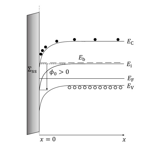
where are the carrier densities in thermal equilibrium, the excess carrier densities in non-equilibrium, and is the intrinsic carrier concentration. We have used where are the quasi-Fermi potentials of electrons and holes. Unless stated otherwise, the subscript 0 stands for a quantity evaluated in thermal equilibrium (), where the equilibrium temperature is assumed as =300 K. Note that where is the Fermi potential of the semiconductor that is determined by the bulk doping concentration which is assumed to be uniform. This implies the following expressions for , which can in turn be interpreted as their definitions
| (12) | |||
The quantity represents the difference between potentials in non-equilibrium and thermal equilibrium. Conversely, . We will call the equilibrium (excess) potential. A graphical representation of the potentials is provided in the energy band diagrams in Fig. 9. Scaling the intrinsic Fermi potential to zero, , the sign convention is that the value of a potential is positive when it lies below , and negative when it is above. Provided the definitions listed above, the set of semiconductor equations is obtained as [36, 39]
| (13) |
where and are the net recombination and generation rates of charge carriers occurring within the bulk, . are the permittivity of free space and the dielectric constant of the semiconductor, and the carrier densities in thermal equilibrium when . Finally, is the intrinsic Debye length, and the Debye length associated with density . We can use for an intrinsic type or for extrinsic p-type (n-type) semiconductors.
The local charge neutrality assumption identifies the excess electron and hole densities throughout the body of the semiconductor (), hence, . Since the total charge density is defined as , this amounts to removing the Poisson equation from the semiconductor equations, and nulling any effects occurring from the total charge distribution. This hinders one from evaluating the exact solution for which is the focus of our study.
Therefore, the global charge neutrality condition, which states that the total charge be conserved within the semiconductor as a whole, is introduced. In order to express this statement quantitatively, we present the appropriate boundary conditions for the free surfaces of a semiconductor. The boundary conditions at the surfaces are determined by the charge carrier flux across the surfaces
| (14) |
These equations determine the gradients of and , or equivalently, the diffusion of excess electrons and holes, at the boundaries. The potential gradients, and are non-zero only in the presence of surface charges or equivalently, surface states. In particular, the excess potential gradient is determined from the general relation
| (15) |
for . Then the global charge neutrality condition is stated as . In the absence of surface charges at , we have . Also, are the net recombination and generation rates of charge carriers occurring at the surface due to certain surface states, if there exist any. We discuss the meaning of these terms thoroughly in section F. Throughout the report, surface charges are assumed to exist only at .
Appendix E The uniform bulk
Assuming no surface effects, the following conditions hold.
| (16) |
We define the bulk recombination rate suitable for the low excitation regime, , where is the recombination coefficient for the semiconductor in its intrinsic state. is interpreted as the effective intrinsic lifetime of charge carriers (in the sense that it is the net effect of the band-to-band, Auger, and Shockley-Read-Hall type recombination processes) and can be treated as a constant for low excitations. Though not completely accurate, this is a good approximation for cases where surface effects are absent, and it can provide sufficient information about how bulk properties of the semiconductor are modified under different effective recombination rates without having to resort to numerical evaluation. The bulk (photo)generation process is assumed to be of Beer-Lambert type, , with the incident photon flux and wavelength-dependent bulk absorption coefficient .
In the low excitation regime, the homogeneous semiconductor equations () for the uniform bulk are reduced to
| (17) | ||||
with the new length parameters introduced in the final equations defined in Table 4.
| Parameter |
|
|
|
|
||||
|---|---|---|---|---|---|---|---|---|
| 0 | ||||||||
| 0 |
The semiconductor type is determined according to the following relation: intrinsic – , p (n)-type – where the big-O notation denotes the order of magnitude of the excess carrier densities. The definition for the intrinsic diffusion lengths is . The extrinsic diffusion lengths are defined as
| (18) |
where may be interpreted as weight factors that modify the intrinsic diffusion lengths to their extrinsic values in doped cases. Note that the Poisson equation has not been removed, but rather absorbed into the continuity equations. Therefore, the equations fully account for charge distribution effects.
The solutions of Eq. (17) can be solved using separation of variables with respect to space and time. Using the ansatz, , we get
| (19) | |||
Now, we substitute into the above equation. Then, . Defining as the constants associated to the separated variables, we obtain a set of equations
| (20) |
Let us consider two limiting cases where we can develop intuition about the general solutions that are to be derived shortly.
E.1 Temporally stationary case
The stationary spatial density of charge carriers may be obtained under the condition, . Recovering in the right-hand side of the equations, we obtain
| (21) | |||
The homogeneous solutions are found with the ansatz, , while the particular solutions can be calculated with the ansatz, . The boundary conditions used to determine the coefficients in the homogeneous solution are
| (22) |
where global charge neutrality is implicit in the above expression. Through some algebra, the total solution is obtained as
| (23) |
where are the spatial mode eigenvalues with
| (24) |
and are the corresponding eigenvectors. These spatial modes are inherent bulk properties of the semiconductor with distinct physical significance. Borrowing terminologies from the reference [krcmar_exact_2002], where such spatial densities have been studied in the context of the Dember effect [23], corresponds to the Debye-screening mode and the diffusion-recombination mode. Note that the total charge density is non-zero, which cannot be derived from local charge neutrality. This implies that even in the absence of externally applied fields, illumination of light can charge a semiconductor. In general, this bulk charging increases with larger absorption coefficients and varies as a function of the material properties such as the intrinsic carrier concentration, carrier mobility, and doping concentration.
E.2 Spatially flat case
The temporal evolution of a spatially flat density can be solved under the condition, . We consider the case where with initially finite carrier densities, . The solutions can be solved for in a similar fashion as the temporally stationary case, which are obtained as
| (25) |
where are the temporal mode eigenvalues,
| (26) |
and are the corresponding eigenvectors. The total charge density can then be expressed as
| (27) |
Again, such an expression cannot be derived under the local charge neutrality condition. As in the temporally stationary case, the time constants associated with the eigenvalues have distinct physical meanings, being the dielectric relaxation time, and the carrier lifetime [roosbroeck_space_1961]. This is because the total charge density relaxes to zero in a characteristic time , whereas the individual charge carrier densities diminish through diffusion and recombination over the characteristic time . It can be interpreted that local charge neutrality () is achieved in time , and that the system returns to thermal equilibrium () in time . Given the relation Eq. (15), the electric field reaches a constant value after . In the absence of surface charges, the field is exactly zero, which means that the system completely neutralizes in the dielectric relaxation time. This is not true in the presence of surface charges. Non-uniform carrier trapping sites in the bulk can also complicate the dynamics. The additional charge equilibration processes introduced by material inhomogeneities or discontinuities of the material can modify the neutralization time from that of a uniform bulk.
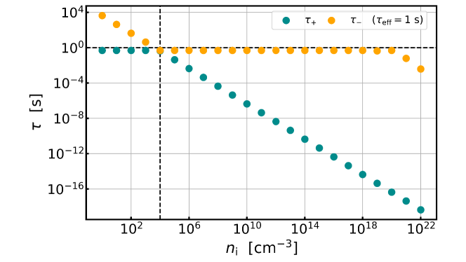
Fig. 10 shows a plot of and defined in Eq. (26) for a hypothetical material as a function of the intrinsic carrier concentration , with the effective carrier lifetime and carrier mobility values set to 1 s and cm V s-1, respectively. The left and right regions of the plot correspond to the insulator (small ) and conductor (large ), while the middle region is indicative of the semiconductor (intermediate ). The maximum value of is set by , indicated as the horizontal dashed line. Values of and determine the location of the crossing point (or degenerate point) between and , shifting the location of the vertical line.
Note that the dielectric relaxation of an unpaired charge density in conductors and insulators is described by the equation
| (28) |
which is basically the continuity equation for inhomogeneous ohmic materials [haus_em_1989]. When the dielectric constant and conductivity is homogeneous throughout the material, the right-hand side of the equation vanishes and the dielectric relaxation time is obtained as . In these systems, there are no dynamics of mobile carriers, in the sense that an initial density relaxes to the boundary without generating a net charge density beyond the initially occupied volume. [haus_em_1989].
E.3 General spatiotemporal solutions
Solving the coupled homogeneous equations Eq. (20) for both space and time, it can be shown that the spatial and temporal modes, 1) the Debye-screening mode () and the dielectric relaxation time (), and 2) the diffusion-recombination mode () and the carrier lifetime (), are directly coupled. This presents a consistent framework for the bulk response of a semiconductor in non-equilibrium. The general solutions are obtained as
| (29) |
where . This expression is a generalization of the limiting case solutions presented in the previous sections. The spatial modes are split into the Debye-screening () and diffusion-recombination () modes to which are associated the characteristic time constants (generalized dielectric relaxation time) and (generalized carrier lifetime), respectively. In order to describe the most general charge carrier dynamics, including a generation process , we can use the Fourier series analysis using the homogeneous solutions and determine the coefficients, .
Appendix F The presence of surface charges
Analytical solutions are not obtainable in the presence of surface charges because space charge quantities in thermal equilibrium are not constant, i.e., , hence rendering the semiconductor equations nonlinear even in the low excitation regime. Therefore, the semiconductor equations Eq. (D) must be solved numerically.
Surface charges typically originate from surface states, and can largely be classified into two categories [33, 34]. The first is fixed surface charge, which is long-term fixed charge that remains stationary during the dynamics of excess charge carriers in non-equilibrium, commonly associated with the slow surface state. The second is charge that originates from the interface state (or fast surface state) which is basically a Shockley-Read-Hall type defect state within the bandgap of the semiconductor localized at the surface that can be exchanged with the bulk. We denote the charge densities associated with the fixed surface charge and interface state as and , respectively. Since nonzero surface charge density gives rise to a potential gradient at the surface, boundary condition values (see equation Eq. (14)) that were nulled in the uniform bulk problem must be recovered. The potential gradient can be decomposed into the equilibrium and excess potential gradients, and then into the contributions from the fixed surface charge and interface state as
| (30) |
where we used , and . A fixed surface charge of results in the equilibrium potential gradient
| (31) |
On the other hand, the interface state is characterized by numerous parameters. Let us consider two types of discrete interface states: an acceptor-type and a donor-type. The acceptor-type is negative (neutral) when occupied by an electron (a hole), whereas the donor-type is neutral (positive) when occupied by an electron (a hole). The potential gradient is given as
| (32) |
where is the electron occupation probability of the interface state. We focus on two processes that may occur through these states, 1) surface recombination and 2) surface absorption (also known as photoionization), in the presence of which the general rate equation associated with is given as [49, 50, 43]
| (33) |
Recall from section D. The trap parameters are the electron and hole surface recombination velocities with dimensions cms-1. and are the capture cross sections and thermal velocities of electrons and holes whose dimensions are cm2 and cms-1, respectively. The concentrations are determined by the energy level of the defect within the bandgap. Introducing the dimensionless surface absorption coefficients where are the optical cross sections for electrons and holes, we define the corresponding surface flux quantities, where is the incident photon flux used previously in the bulk generation process . The theory of optical cross sections is presented in the next section. The terms describe surface recombination, or capturing of free charge carriers from the bulk into the interface states, whereas denote the release of captured charge carriers into the bulk. In particular, the first and second terms in indicate thermal emission and optical generation rates, respectively, where the latter corresponds to surface absorption or photoionization [43]. Here, we limit our analysis to steady state solutions, , which results in a steady state value for the electron occupation probability and net charge carrier flow rate as
| (34) |
where . In the presence of the interface states, then, the boundary value of the excess potential gradient is modified as
| (35) |
with . Fixed surface charges do not contribute to this quantity since they are stationary and thus cancel out. Global charge neutrality must apply in order to balance charge transfer between the surface and bulk. This is naturally embedded in the relation
| (36) |
which is just equation Eq. (15) expressed in terms of equation Eq. (35). Equipped with the extended boundary conditions for and , the steady state solutions of the semiconductor equations can be readily obtained using numerical methods.
Appendix G Surface absorption and the optical cross section
Here, we briefly summarize the theoretical results presented in Ref. [56, 57]. The ground state wave function of the Hulthén potential Eq. (LABEL:eqn_hulthen) is
| (37) |
The photoionization cross section, in terms of the photon energy , is obtained as
| (38) |
where is the effective field ratio, the frequency-dependent refractive index, the dielectric constant of the material, the fine structure constant, and is the ionization energy between the defect level and the conduction band edge. We assume [52], and replace with an approximate average value of 4 for the experimental wavelengths [pierce_optical_1972, aspnes_optical_1983]. The parameter is defined as where is the effective mass of the optically excited particle, which in our case, is the electron, . In our calculations, we use [60].
Appendix H The simulation geometry and estimation of the SPV
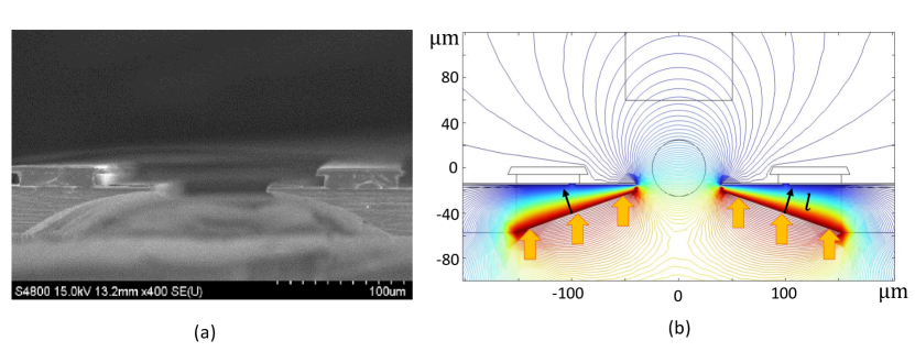
In order to estimate the magnitude and sign of the stray field generated at the position of the trapped ion due to the SPV, an electrostatic analysis was performed using the COMSOL software by imposing voltages on the inclined surfaces of the exposed silicon substrate of the ion trap (see Fig. 11 (b)). The geometry for COMSOL simulations was extracted from the Scanning-electron-microscope (SEM) image shown in Fig. 11 (a). A voltage of +1 V at the silicon surface generated an electric field of +1055 Vm -1 at the position of the ion. On the other hand, +1 V applied to the inner dc electrode pairs produced an electric field of +2880 Vm -1 at the ion position. The experimental values of the SPV could be estimated systematically by multiplying this ratio, 2880/10552.73, to the absolute value of the compensation voltages.
Appendix I Alternative mechanism for the observed ion displacement and limitations of the model
Here we discuss an 1) alternative mechanism for the ion displacement and 2) the limitations of our photoconductive charging model.
I.1 Alternative mechanism
We consider an additional SPV mechanism that can produce a positive stray field at the position of the ion. Positive photovoltage can be induced by a purely bulk response of the semiconductor (see section E). In particular, when the carrier mobilities satisfy , which is true for silicon, the underlying charge density resembles that of a dipole with the positive side facing the surface of illumination (the Dember effect). The magnitude of the photovoltage, however, is small and decreases with increasing doping concentration due to enhanced screening (reduction in the Debye-screening length). In addition, the dielectric relaxation time, which is the characteristic time at which the semiconductor bulk neutralizes when light is turned off, is much shorter than the observed time scale at which the ion returns to its equilibrium position (1 to 100 µs). For p-type silicon doped with a concentration of 1015 cm-3, the magnitude and relaxation time of the photovoltage are on the order of 10 mV and 10 ps, respectively.
Moreover, numerical simulations show that any mechanism dominated by bulk absorption predicts larger magnitudes of SPV at shorter wavelengths in accordance with the bulk absorption spectrum of silicon, failing to explain the spectral response of the observed SPV. Only in the presence of the proposed interface states can the magnitude, sign, and wavelength dependence of the SPV be comprehended consistently. Although this effect is small in our system, the photovoltage may still be problematic in others depending on doping concentration and the proximity of the trapped ion to the charged volume.
I.2 Limitations of the photoconductive charging model
The following list states some limitations of our photoconductive charging model.
1. Interface states have been assumed to occupy a single discrete energy level, while in more realistic systems, they would more likely form a distribution within the bandgap, in which case the observations would be more of a collective response. Although the former assumption allows for an effective explanation and a more tractable computation, future work may be devoted to studying more generalized surface conditions involving a distribution of interface states.
2. The theory of photoionization from bulk defects has been applied to surface defects. Although a complete theory for the optical excitation of surface defects is lacking [23], the optical cross section of a delta-function defect as a function of the distance from a surface has been studied in Ref. [chazalviel_abs_1987], showing a tendency in the optical cross section spectrum to broaden, while its peak value is shifted to larger photon energies, as the defect becomes closer to the surface. The fitted values of and in the Hulthén potential may be slightly modified if such effects are included in the model. Since the overall spectral dependence of the SPV observed in our experiments are explained well by that derived for bulk defects, we suspect the optically responsive interface states to have originated from RIE-induced defects that penetrated deep enough into the substrate to have spectral properties resembling that of the bulk defect, but sufficiently localized at the surface (i.e., within a few atomic layers to several nm’s, which is much smaller than the Debye-screening length and the absorption depth of any incident light) so that their effects are manifest as boundary conditions in the context of the semiconductor equations.
3. We have assumed a slab model, but this may not be able to fully describe the real exposed surface of the silicon substrate which is a more complicated three-dimensional structure. One justification for using the slab model was based on the numerical simulation results that were insensitive to a variation of the slab thickness l as long as it was much larger than the initial surface depletion layer (1 µm). However, even in this case, edge effects or diffusion and drift in spatial dimensions other than in the direction of incidence of light were neglected.
4. External field effects have been neglected from the model. This was justified by the experimental fact that the sign and magnitude of the SPV were independent of the changes in voltages applied to the dc electrodes in the vicinity of the exposed semiconductor surface.
Appendix J Simulation of the quantum dynamics
Here, the theory used for simulations of the Rabi oscillation and Bloch sphere trajectory is presented.
J.1 Lindblad master equation
The trapped ion is a composite system, involving the qubit and oscillator degrees of freedom. Its density matrix can be expressed as where is the qubit state corresponding to the subspace formed by the oscillator eigenstates and . When the oscillator is coupled to a phonon bath via an amplitude damping channel described by the Lindblad operator, , the Lindblad master equation can be formulated as [gardiner_1989]
| (39) | ||||
where is the system Hamiltonian, is the heating rate, and is the mean phonon number of the phonon bath evaluated in terms of the oscillator states. We set the initial condition as where the qubit state is initialized to and the oscillator state has a thermal distribution about the mean phonon number . We propagate the state through time using the update rule, , and obtain the reduced density matrix describing the qubit state by taking the partial trace over the oscillator states, .
J.2 Position operator of the time-dependent oscillator
The theory of forced time-dependent oscillators presented in Refs.[ji_1995, ji_1996] is applied to the linear Paul trap. The Hamiltonian for the oscillator degree of freedom of the trapped ion is given as
| (40) |
where describes the dynamically trapped ion, and is an externally driven force. is the mass of the ion. In the subsequent derivations, the Planck constant is set to , but recovered in the final expressions. In this system, the position operator in the Heisenberg picture is obtained as
| (41) |
where are the raising(lowering) operators of a reference oscillator defined at , and is an invariant of motion, defined as
| (42) |
The parameters are determined from the coupled first-order differential equations
| (43) |
The time-dependent frequency is obtained as
| (44) |
while the displacement is derived as
| (45) |
With the definition of for the linear Paul trap
| (46) |
where are Mathieu equation parameters [leibfried_quantum_2003], we obtain the solutions for in terms of a single function as
| (47) |
The function and its conjugate are solutions to the Mathieu equation
| (48) |
subject to the initial conditions and [glauber_quantum]. It follows that , which is interpreted as the secular frequency of the trapped ion. The lowest order solution () is found to be
| (49) |
which can be substituted into Eq. (47) to obtain
| (50) |
Recovering , we obtain
| (51) |
with
| (52) |
and
| (53) |
Finally, we neglect the squeezing factor linked to intrinsic micromotion by making the approximation
| (54) |
in Eqs. (51) and (52). This cannot be applied to the factor in the integral in Eq. (53) since it would amount to removing the effects of excess micromotion as well.
References
- Stick et al. [2006] D. Stick, W. K. Hensinger, S. Olmschenk, M. J. Madsen, K. Schwab, and C. Monroe, Ion trap in a semiconductor chip, Nat.Physics 2, 36 (2006).
- Bermudez et al. [2017] A. Bermudez, X. Xu, R. Nigmatullin, J. O’Gorman, V. Negnevitsky, P. Schindler, T. Monz, U. G. Poschinger, C. Hempel, J. Home, et al., Assessing the Progress of Trapped-Ion Processors Towards Fault-Tolerant Quantum Computation, Phys. Rev.X 7, 041061 (2017).
- Jain et al. [2020] S. Jain, J. Alonso, M. Grau, and J. P. Home, Scalable Arrays of Micro-Penning Traps for Quantum Computing and Simulation, Phys. Rev.X 10, 031027 (2020).
- Romaszko et al. [2020] Z. D. Romaszko, S. Hong, M. Siegele, R. K. Puddy, F. R. Lebrun-Gallagher, S. Weidt, and W. K. Hensinger, Engineering of microfabricated ion traps and integration of advanced on-chip features, Nat. Rev.Physics 2, 285 (2020).
- Akhtar et al. [2023] M. Akhtar, F. Bonus, F. R. Lebrun-Gallagher, N. I. Johnson, M. Siegele-Brown, S. Hong, S. J. Hile, S. A. Kulmiya, S. Weidt, and W. K. Hensinger, A high-fidelity quantum matter-link between ion-trap microchip modules, Nat.Communications 14, 531 (2023).
- Pino et al. [2021] J. M. Pino, J. M. Dreiling, C. Figgatt, J. P. Gaebler, S. A. Moses, M. S. Allman, C. H. Baldwin, M. Foss-Feig, D. Hayes, K. Mayer, et al., Demonstration of the trapped-ion quantum CCD computer architecture, Nature 592, 209 (2021).
- Niffenegger et al. [2020] R. J. Niffenegger, J. Stuart, C. Sorace-Agaskar, D. Kharas, S. Bramhavar, C. D. Bruzewicz, W. Loh, R. T. Maxson, R. McConnell, D. Reens, et al., Integrated multi-wavelength control of an ion qubit, Nature 586, 538 (2020).
- Mehta et al. [2020] K. K. Mehta, C. Zhang, M. Malinowski, T.-L. Nguyen, M. Stadler, and J. P. Home, Integrated optical multi-ion quantum logic, Nature 586, 533 (2020).
- Ivory et al. [2021] M. Ivory, W. J. Setzer, N. Karl, H. McGuinness, C. DeRose, M. Blain, D. Stick, M. Gehl, and L. P. Parazzoli, Integrated Optical Addressing of a Trapped Ytterbium Ion, Phys. Rev.X 11, 041033 (2021).
- Turchette et al. [2000a] Q. A. Turchette, Kielpinski, B. E. King, D. Leibfried, D. M. Meekhof, C. J. Myatt, M. A. Rowe, C. A. Sackett, C. S. Wood, W. M. Itano, et al., Heating of trapped ions from the quantum ground state, Phys. Rev.A 61, 063418 (2000a).
- Turchette et al. [2000b] Q. A. Turchette, C. J. Myatt, B. E. King, C. A. Sackett, D. Kielpinski, W. M. Itano, C. Monroe, and D. J. Wineland, Decoherence and decay of motional quantum states of a trapped atom coupled to engineered reservoirs, Phys. Rev.A 62, 053807 (2000b).
- Schriefl et al. [2006] J. Schriefl, Y. Makhlin, A. Shnirman, and G. Schön, Decoherence from ensembles of two-level fluctuators, New J. Physics 8, 1 (2006).
- Safavi-Naini et al. [2011] A. Safavi-Naini, P. Rabl, P. F. Weck, and H. R. Sadeghpour, Microscopic model of electric-field-noise heating in ion traps, Phys. Rev.A 84, 023412 (2011).
- Kumph et al. [2016] M. Kumph, C. Henkel, P. Rabl, M. Brownnutt, and R. Blatt, Electric-field noise above a thin dielectric layer on metal electrodes, New J. Physics 18, 023020 (2016).
- Boldin et al. [2018] I. A. Boldin, A. Kraft, and C. Wunderlich, Measuring Anomalous Heating in a Planar Ion Trap with Variable Ion-Surface Separation, Phys. Rev.Letters 120, 023201 (2018).
- Lee et al. [2023] W. Lee, D. Chung, J. Kang, H. Jeon, C. Jung, D.-I. D. Cho, and T. Kim, Micromotion compensation of trapped ions by qubit transition and direct scanning of dc voltages, OpticsExpress 31, 33787 (2023).
- Harlander et al. [2010] M. Harlander, M. Brownnutt, W. Hänsel, and R. Blatt, Trapped-ion probing of light-induced charging effects on dielectrics, New J. Physics 12, 093035 (2010).
- Wang et al. [2011] S. X. Wang, G. Hao Low, N. S. Lachenmyer, Y. Ge, P. F. Herskind, and I. L. Chuang, Laser-induced charging of microfabricated ion traps, J. Appl.Physics 110, 104901 (2011).
- Härter et al. [2014] A. Härter, A. Krükow, A. Brunner, and J. Hecker Denschlag, Long-term drifts of stray electric fields in a Paul trap, Appl. Phys.B 114, 275 (2014).
- Doret et al. [2012] S. C. Doret, J. M. Amini, K. Wright, C. Volin, T. Killian, A. Ozakin, D. Denison, H. Hayden, C. Pai, and R. E. Slusher, Controlling trapping potentials and stray electric fields in a microfabricated ion trap through design and compensation, New J. Physics 14, 073012 (2012).
- Hong et al. [2017] S. Hong, Y. Kwon, C. Jung, M. Lee, T. Kim, and D.-i. D. Cho, A new microfabrication method for ion-trap chips that reduces exposure of dielectric surfaces to trapped ions, J. MicroelectromechanicalSystems 27, 28 (2017).
- Jung et al. [2023] C. Jung, J. Jeong, S. Yoo, T. Kim, and D. D. Cho, Method for Estimating Locations of Laser-Induced Stray Charges on Surface-Electrode Ion Traps Using Secular Frequency Shift at Multiple Ion Positions, Phys. Rev.Applied 20, 014032 (2023).
- Kronik [1999] L. Kronik, Surface photovoltage phenomena: theory, experiment, and applications, Surf. ScienceReports 37, 1 (1999).
- Brown et al. [2021] K. R. Brown, J. Chiaverini, J. M. Sage, and H. Häffner, Materials challenges for trapped-ion quantum computers, Nat. Rev.Materials 6, 892 (2021).
- Stick et al. [2010] D. Stick, K. Fortier, R. Haltli, C. Highstrete, D. Moehring, C. Tigges, and M. Blain, Demonstration of a microfabricated surface electrode ion trap, arXiv preprintarXiv:1008.0990 (2010).
- Jung et al. [2021] C. Jung, W. Lee, J. Jeong, M. Lee, Y. Park, T. Kim, and D.-I. ”Dan” Cho, A microfabricated ion trap chip with a sloped loading slot to minimize exposing trapped ions to stray charges, Quantum Science Technology 6, 044004 (2021).
- Blain et al. [2021] M. G. Blain, R. Haltli, P. Maunz, C. D. Nordquist, M. Revelle, and D. Stick, Hybrid MEMS-CMOS ion traps for NISQ computing, Quantum Science Technology 6, 034011 (2021).
- Niedermayr [2015] M. Niedermayr, Cryogenic surface ion traps, Ph.D. thesis, Universität Innsbruck (2015).
- Lakhmanskiy [2019] K. Lakhmanskiy, On heating rates in cryogenic surface ion traps, Ph.D. thesis, Universität Innsbruck (2019).
- Mehta et al. [2014] K. K. Mehta, A. M. Eltony, C. D. Bruzewicz, I. L. Chuang, R. J. Ram, J. M. Sage, and J. Chiaverini, Ion traps fabricated in a CMOS foundry, Appl. Phys.Letters 105, 044103 (2014).
- Niedermayr et al. [2014] M. Niedermayr, K. Lakhmanskiy, M. Kumph, S. Partel, J. Edlinger, M. Brownnutt, and R. Blatt, Cryogenic surface ion trap based on intrinsic silicon, New J. Physics 16, 113068 (2014).
- Schroder [2001] D. K. Schroder, Surface voltage and surface photovoltage: history, theory and applications, Measurement Science Technology 12, R16 (2001).
- Garrett and Brattain [1955] C. G. B. Garrett and W. H. Brattain, Physical Theory of Semiconductor Surfaces, Phys.Review 99, 376 (1955).
- Johnson [1958] E. O. Johnson, Large-Signal Surface Photovoltage Studies with Germanium, Phys.Review 111, 153 (1958).
- Łagowski et al. [1971] J. Łagowski, C. L. Balestra, and H. C. Gatos, Photovoltage inversion effect and its application to semiconductor surface studies: CdS, Surf.Science 27, 547 (1971).
- Van Roosbroeck [1950] W. Van Roosbroeck, Theory of the flow of electrons and holes in Germanium and other semiconductors, Bell System TechnicalJournal 29, 560 (1950).
- Nicollian and Goetzberger [1967] E. H. Nicollian and A. Goetzberger, The Si-SiO2 Interface — Electrical Properties as Determined by the Metal-Insulator-Silicon Conductance Technique, Bell System TechnicalJournal 46, 1055 (1967).
- Cheng [1977] Y. C. Cheng, Electronic states at the silicon-silicon dioxide interface, Prog. In Surf.Science 8, 181 (1977).
- Kingston and Neustadter [1955] R. H. Kingston and S. F. Neustadter, Calculation of the Space Charge, Electric Field, and Free Carrier Concentration at the Surface of a Semiconductor, J. Appl.Physics 26, 718 (1955).
- Garrett and Brattain [1956] C. G. B. Garrett and W. H. Brattain, Distribution and cross-sections of fast states on Germanium surfaces, Bell System TechnicalJournal 35, 1041 (1956).
- Bebb and Chapman [1967] H. B. Bebb and R. A. Chapman, Application of quantum defect techniques to photoionization of impurities in semiconductors, J. Phys. Chemistry Solids 28, 2087 (1967).
- Chaudhuri [1982] S. Chaudhuri, Optical-transition cross sections involving impurities in semiconductors, Phys. Rev.B 26, 6593 (1982).
- Hsieh and Card [1989] Y. K. Hsieh and H. C. Card, Limitation to Shockley–Read–Hall model due to direct photoionization of the defect states, J. Appl.Physics 65, 2409 (1989).
- Leibovitch et al. [1994] M. Leibovitch, L. Kronik, E. Fefer, and Y. Shapira, Distinction between surface and bulk states in surface-photovoltage spectroscopy, Phys. Rev.B 50, 1739 (1994).
- Matsumoto and Sugano [1982] H. Matsumoto and T. Sugano, Characterization of Reactive Ion Etched Silicon Surface by Deep Level Transient Spectroscopy, J. ElectrochemicalSociety 129 (1982).
- Gatzert et al. [2006] C. Gatzert, A. W. Blakers, P. N. K. Deenapanray, D. Macdonald, and F. D. Auret, Investigation of reactive ion etching of dielectrics and Si in CHF3/O2 or CHF3/Ar for photovoltaic applications, J. Vac. Science TechnologyA 24, 1857 (2006).
- Mohammed [2005] S. S. Mohammed, Investigation of surface states and device surface charging in nitride materials using scanning Kelvin probe microscopy, Ph.D. thesis, Virginia Commonwealth University (2005).
- Maltby et al. [1975] J. Maltby, C. Reed, and C. Scott, Analysis of the surface photovoltaic effect in photoconductors: CdS, Surf.Science 51, 89 (1975).
- Shockley and Read [1952] W. Shockley and W. T. Read, Statistics of the Recombinations of Holes and Electrons, Phys.Review 87, 835 (1952).
- Hall [1952] R. N. Hall, Electron-Hole Recombination in Germanium, Phys.Review 87, 387 (1952).
- Lucovsky [1965] G. Lucovsky, On the photoionization of deep impurity centers in semiconductors, Solid StateCommunications 3, 299 (1965).
- Anderson [2008] W. W. Anderson, Shallow impurity states in semiconductors: Absorption cross-sections, excitation rates, and capture cross-sections, Solid-StateElectronics 18, 235 (2008).
- Stoneham [1979] A. M. Stoneham, Phonon coupling and photoionisation cross-sections in semiconductors, J. Phys. C: Solid StatePhysics 12, 891 (1979).
- Olejníková et al. [1981] B. Olejníková, . Hrivnák, and M. Kedro, The model potential for charged centres in semiconductors, Phys. Status SolidiB 107, 451 (1981).
- Coon and Karunasiri [1986] D. D. Coon and R. P. G. Karunasiri, Green’s-function–quantum-defect treatment of impurity photoionization in semiconductors, Phys. Rev.B 33, 8228 (1986).
- Ilaiwi and Tomak [1990] K. Ilaiwi and M. Tomak, Impurity photoionization in semiconductors, J. Phys. Chemistry Solids 51, 361 (1990).
- Tomak [1982] M. Tomak, On the photo-ionization of impurity centres in semiconductors, Tech. Rep. (International Centre for Theoretical Physics, 1982).
- Campbell et al. [2010] W. C. Campbell, J. Mizrahi, Q. Quraishi, C. Senko, D. Hayes, D. Hucul, D. N. Matsukevich, P. Maunz, and C. Monroe, Ultrafast Gates for Single Atomic Qubits, Phys. Rev.Letters 105, 090502 (2010).
- Siegfried [2011] S. Siegfried, Analysis and Simulation of Semiconductor Devices (Springer Vienna, 2011).
- Chenming [2009] C. H. Chenming, Modern Semiconductor Devices for Integrated Circuits (Pearson, 2009).
- Arora et al. [1982] N. Arora, J. Hauser, and D. Roulston, Electron and hole mobilities in silicon as a function of concentration and temperature, IEEE Transactions on ElectronDevices 29, 292 (1982).
- Green [2008] M. A. Green, Self-consistent optical parameters of intrinsic silicon at 300K including temperature coefficients, Sol. Energy Mater. Sol.Cells 92, 1305 (2008).
- Böer and Pohl [2023] K. W. Böer and U. W. Pohl, Semiconductor Physics (Springer Nature, 2023).
- Alekperov [1998] O. Z. Alekperov, Capture of carriers by screened charged centres and low-temperature shallow-impurity electric field breakdown in semiconductors, J. Physics: CondensedMatter 10, 8517 (1998).
- Tong and Lam [1976] K. Y. Tong and Y. W. Lam, Difficulties in observing direct optical excitation of Si-SiO2 interface states, J. Phys.