Facilitating Atom Probe Tomography of 2D MXene Films by In Situ Sputtering
Abstract
2D materials are emerging as promising nanomaterials for applications in energy storage and catalysis. In the wet chemical synthesis of MXenes, these 2D transition metal carbides and nitrides are terminated with a variety of functional groups, and cations such as \ceLi+ are often used to intercalate into the structure to obtain exfoliated nanosheets. Given the various elements involved in their synthesis, it is crucial to determine the detailed chemical composition of the final product, in order to better assess and understand the relationships between composition and properties of these materials. To facilitate atom probe tomography analysis of these materials, a revised specimen preparation method is presented in this study. A colloidal \ceTi3C2T_z MXene solution was processed into an additive-free free-standing film and specimens were prepared using a dual beam scanning electron microscope / focused ion beam. To mechanically stabilize the fragile specimens, they were coated using an in situ sputtering technique. As various 2D material inks can be processed into such free-standing films, the presented approach is pivotal for enabling atom probe analysis of other 2D materials.
Keywords
atom probe tomography, focused ion beam, in situ coating, 2D materials, MXenes
Introduction
Since the groundbreaking experimental observation of graphene [38], there has been significant interest in 2D materials and their fascinating functional properties. Following graphene, the successful synthesis of other 2D elemental materials [33], 2D transition metal dichalcogenides [34] and 2D perovskites [23], to name a few, has significantly expanded the landscape of 2D materials. Because 2D materials have a thickness of one up to a few atomic layers, and thus a high surface-to-volume ratio, they are particularly interesting for applications involving highly surface-active chemical processes, such as energy storage or catalysis [37].
MXenes, 2D transition metal carbides and nitrides, have also been the subject of intense research since their discovery by the Barsoum and Gogotsi groups [36]. To date, more than 50 different compositions have been synthesized, not even considering the different and highly variable surface chemistries [57, 3]. Their top-down synthesis involves two steps, namely the harsh selective etching of the A layer (typically \ceAl, \ceSi or \ceGa) from a bulk MAX phase(-like) precursor in a typically \ceHF-based wet chemical environment, and the subsequent exfoliation of the obtained weakly bonded multilayer MXenes into individual nanosheets by intercalation of cations or molecules [2, 29]. The general chemical formula of MXenes is written as \ceM_n+1X_nT_z, characterized by atomic layers of one or more early transition metals M and interleaved atomic layers of \ceC and/or \ceN, denoted as X, where \ceT_z represents surface termination groups saturating the bare surface during synthesis. Because this synthesis process is scalable [51], and the MXene nanosheets can be easily processed into free-standing films [61] or printable inks [60], they are attractive and accessible for industrial applications.
The obtained properties are significantly influenced by the detailed synthesis parameters [54], which control in particular the flake size, defect density and surface chemistry. A carefully optimized synthesis route can therefore be used to fine-tune the properties of the MXenes, which is comparable to defect engineering in bulk materials [27]. However, Shuck pointed out that MXenes are unfortunately often treated as chemicals rather than materials, because the detailed synthesis route is overlooked [50]. For example, in many synthesis protocols for \ceTi3C2T_z, the most studied MXene to date, spontaneous intercalation of \ceLi cations [32] is crucial for obtaining large and high-quality, i.e. less defective, monolayer MXene flakes [13, 30, 45, 48]. Although it is known that the presence of \ceLi influences the properties of the MXenes [5], it remains a difficult task to localize and quantify \ceLi in the material using the commonly applied techniques [49].
Atom Probe Tomography (APT) is an analytical characterization technique with sensitivity to both light and heavy elements and sufficient spatial resolution to address these unanswered questions [12]. Briefly summarized, the atom probe is a time-of-flight mass spectrometer equipped with a position-sensitive detector, where individual atomic or molecular ions are field evaporated from the apex of a sharp, needle-shaped specimen. In combination, the recorded time-of-flight and the impact coordinates of the ions on the detector, allow compositional mapping with a sub-nanometer spatial resolution in 3D [6]. Given these capabilities, APT has been increasingly used in recent years to characterize functional nanomaterials, such as nanoparticles for catalysis, as it provides unique compositional insights that enable an understanding of the activity and degradation of these materials [26].
A critical step towards the APT analysis of nanostructures, including nanoparticles, nanosheets and nanowires, was the development of appropriate specimen preparation approaches, as these materials, unlike bulk materials, do not allow straightforward traditional protocols to prepare needle-shaped specimens [11]. Common workarounds include the deposition of nanoparticles on pre-sharpened needles by electrophoresis [53], or the fixation of nanoparticles with a micromanipulator and subsequent coating on a support [7] followed by sharpening by focused ion beam (FIB) milling. Attachment on pre-sharpened needles combined with a coating has also been proposed [15]. The deposition of a dense matrix material encapsulating the nanoparticles by atomic layer deposition [24] or metallic electrodeposition [17] enables the utilization of the commonly used specimen preparation using a dual beam scanning electron microscope (SEM)-FIB [55]. In the case of nanowires, their needle-like shape may even allow them to be analyzed without special specimen preparation in an atom probe with a local electrode [39, 10].
Despite the wide range of compositions available, and the increasing intensity of research on nanostructures, 2D materials such as MXenes have rarely been investigated using APT. Although graphene is occasionally used to coat biological or liquid APT specimens [1, 43, 44, 42], the analysis of graphene is only incidental. Previous studies have shown how APT can advance our understanding on the detailed composition of 2D materials, such as the incorporation of impurity elements during the wet chemical synthesis of 2D \ceMoS2 [18], or the influence of alkali elements from synthesis on the oxidation of \ceTi3C2T_z MXenes [22]. In both cases, the nanosheets were embedded in a metallic matrix, but they are very difficult to localize for targeted sample preparation, and the small number of nanosheets in an average data set limits the statistics.
Here, APT analysis is performed by taking advantage of the possibility to process MXenes into free-standing films, i.e. a macroscopic stack of nanosheets with the same orientation held together by weak intermolecular forces such as van der Waals forces or hydrogen bonds. APT specimens of a free-standing \ceTi3C2T_z MXene film were prepared by FIB lift-out. Following sharpening, APT specimens were coated in situ by ion milling a \ceCr lamella as sputter target [58], to mechanically stabilize the fragile specimens. In addition to enhanced yield, performance, and increased field-of-view [47], as well as the reduction of artifacts in the analysis of Li-containing materials [52], the presented workflow involving the in situ coating technique may also be a starting point for a simplified and straightforward APT analysis of 2D materials.
Materials and Methods
Synthesis of \ceTi3AlC2 MAX Phase
Ti3AlC2 MAX phase was synthesized by solid–liquid reaction. Briefly, \ceTiC (, Alfa Aesar), \ceTi (, Strem) and \ceAl (, Strem) powders were ball milled at for a duration of . The resulting powder mixture was cold pressed and then heat treated in a furnace at for a period of under a protective \ceAr environment. Finally, the sintered \ceTi3AlC2 MAX phase was ball milled at for to a fine powder, ready for MXene synthesis.
Synthesis of \ceTi3C2T_z MXenes
For \ceTi3C2T_z MXene synthesis, \ceLiF (, Strem) was dissolved in concentrated \ceHCl (, Bio-Lab) in a high density polyethylene vial, to prepare the etchant for selective etching of the \ceAl layer from the previous sintered \ceTi3AlC2 MAX phase. Etching was done by slowly adding of the MAX phase powder to the solution under constant stirring with a magnetic stirrer at degrees for .
After etching, the complete solution was transferred to a centrifuge tube and filled with deionized water (conductivity ). The solution was shaken thoroughly and then centrifuged at for a duration of . The supernatant was decanted, and the remaining sediment was replenished with deionized water, shaken and centrifuged again. Washing was repeated several times until the solution reached a near-neutral pH value, i.e. greater than 6. After washing, the tube containing the sediment was refilled with deionized water and the solution was sonicated in an ice bath for to prevent heating. To remove unetched residues of the MAX phase, the solution was centrifuged at for and the black colloidal supernatant containing single layer MXenes was collected. Finally, the colloidal solution with a yield of about was stored at .
Preparing Free-Standing \ceTi3C2T_z MXene Film
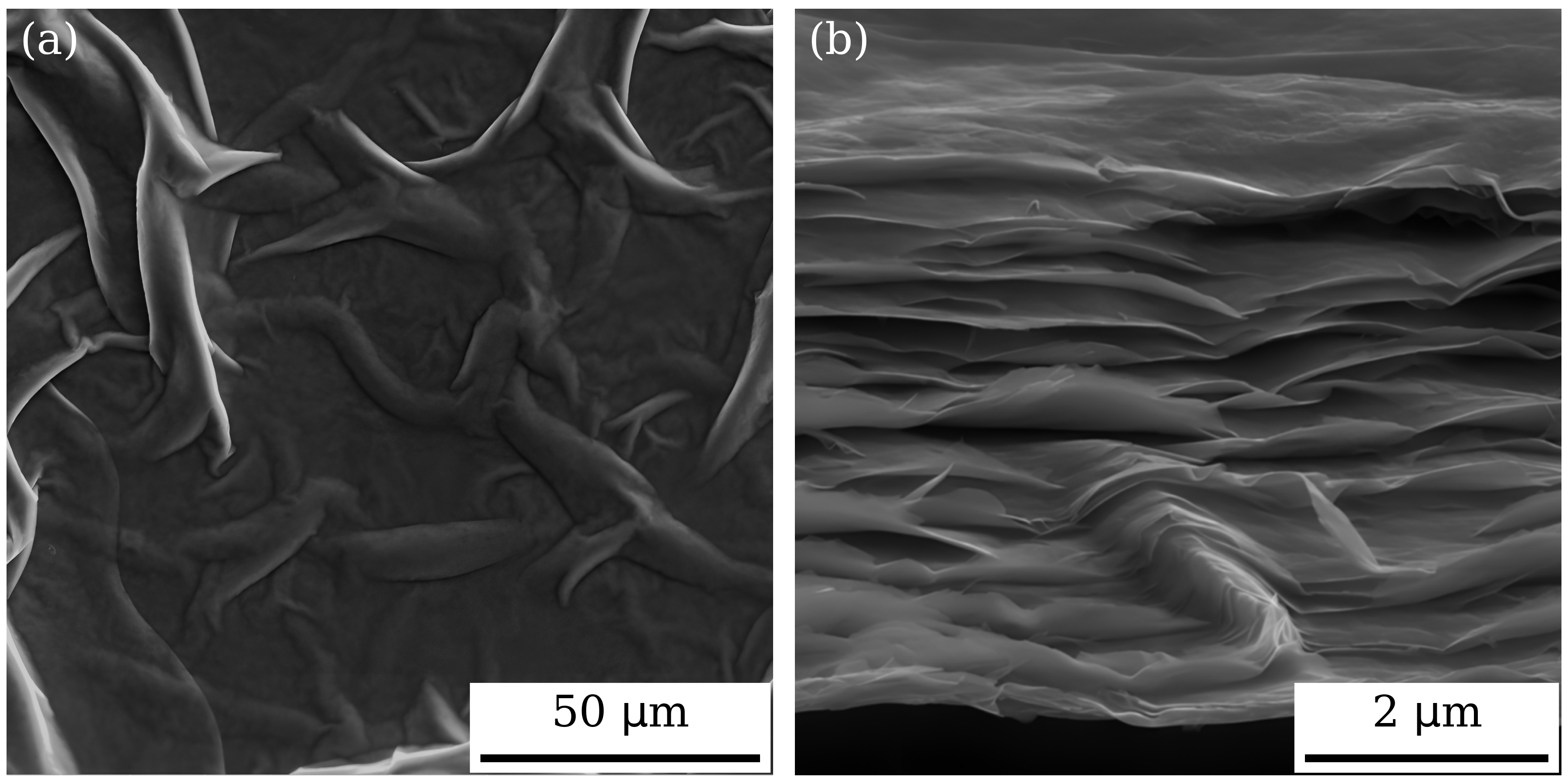
The free-standing MXene film was prepared by vacuum filtration. of the colloidal solution was poured into a vacuum filtration system using a Celgard® membrane. After filtration, the film was removed from the membrane. Figure 1 shows both the top (a) and the cross-sectional view (b) of the free-standing film, revealing the horizontal alignment of the nanosheets in the stack.
APT Specimen Preparation
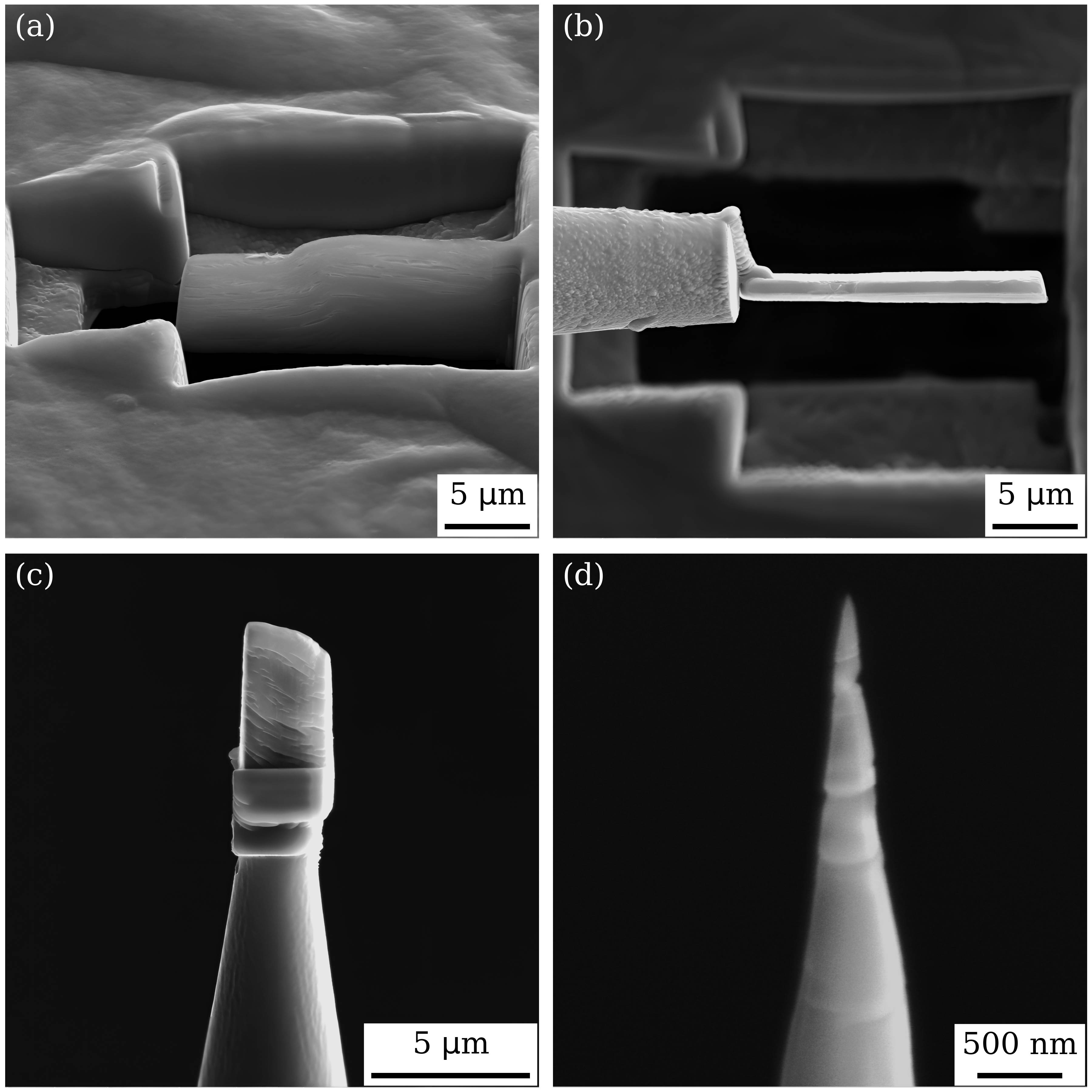
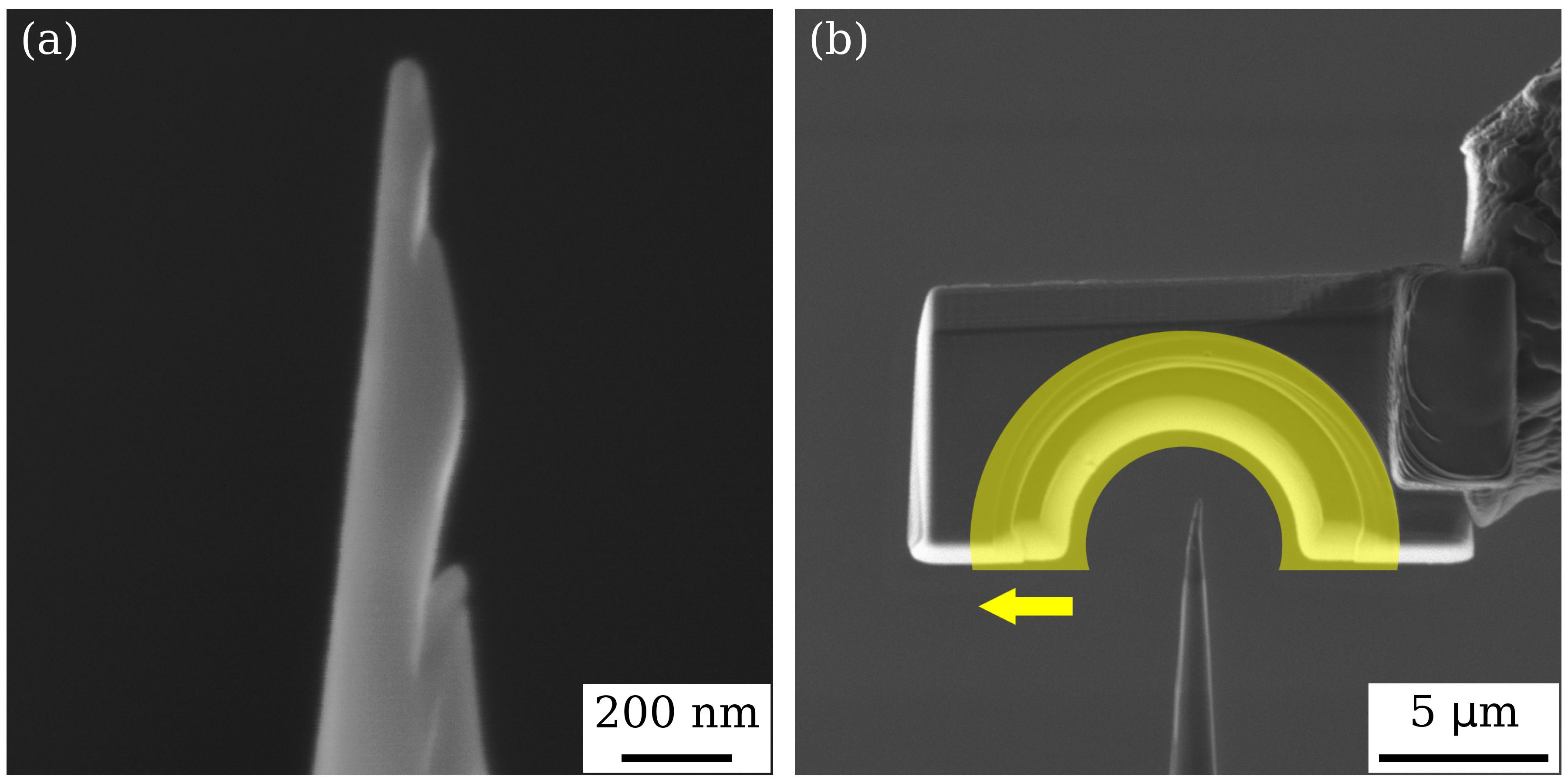
A first batch of needle-shaped APT specimens was prepared from the free-standing MXene film according to the lift-out and sharpening protocol introduced by [55], using a dual beam SEM-FIB (Helios Nanolab 600, FEI) equipped with a \ceGa ion source, as illustrated in Figure 2 (a) - (d). For a second batch of samples, the lift-out was first attached to a needle able to rotate the lifted-out lamella by , thereby aligning the MXene nanosheets more favourably for APT analysis, and then picked up again with the micromanipulator to continue with common specimen preparation. After annular ion milling, specimens such as in Figure 3 (a) were then additionally coated with \ceCr (, small leftover of the synthesis of larger ingots from the workshop at the Max-Planck-Institut für Eisenforschung) using an in situ sputtering technique described by [58], building on previous reported works [21, 9], and as depicted in Figure 3 (b). More details on the complete coating workflow can be found in [47]. Sputtering parameters for the ion beam pattern were and for , repeated times after rotating the specimen each time to ensure a uniform coating. \ceCr as a coating material was chosen in first place for its well-known adhesion properties.
APT Characterization
APT analyses were performed using either a 5000XS (straight flight path) or a 5000XR (reflectron-fitted) local electrode atom probe (Cameca Instruments), operating in ultraviolet ( ) laser-pulsing mode. Parameters were set to a base temperature of , a laser pulse energy varied between and , a laser pulsing rate of , and a target detection rate of ions per pulses on average. Data reconstruction and analysis was done with AP Suite 6.3 by Cameca Instruments following the default voltage-based reconstruction algorithm.
Results and Discussion
Mechanical Instability and In Situ Delithiation
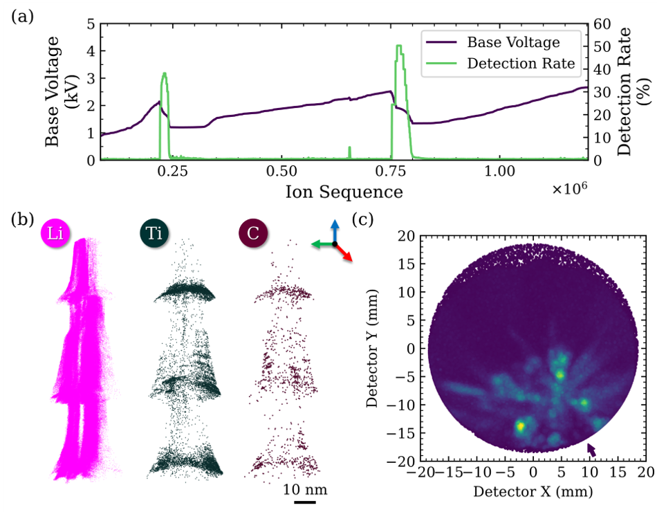
Initial attempts to analyze APT specimens of the free-standing MXene film, prepared as described in Figure 4, faced significant problems with the mechanical stability of the specimens, that may be inherent in the APT analysis of such materials. In this arrangement, the stacking orientation of the nanosheets is perpendicular to the main axis of the APT specimen, as visible in Figure 2 (d). Despite the intermolecular interactions between the MXenes nanosheets, they are not strong enough to withstand the high Maxwell stresses arising from the intense electrostatic field applied during the analysis. In addition, there may also be nanovoids between the nanosheets, as visible in the cross-sectional view of the free-standing film in Figure 1 (b), where intermolecular forces will be almost absent. This results in multiple small fractures, as evidenced by drops in the base voltage curve in Figure 4 (a), which can be explained by a sudden increase in the detection rate due to the detection of several nanosheets breaking off from the specimen apex in very close succession. In almost all cases, measurements are limited to less than a million ions detected before the specimens fractures completely from the silicon support, so the success rate for these samples is rather low.
Li was normally only used in the wet chemical synthesis for exfoliation. However, here up to \ceLi was measured in the analyzed specimens. In the reconstructed 3D atom map in Figure 4 (b), it was observed that at the beginning and after each microfracture, \ceLi field evaporates first before other species such as \ceTi are also detected. During APT analysis, the intense electrostatic field can cause preferential migration of \ceLi atoms [14], also known as in situ delithiation [41], which is a known artifact in the analysis of \ceLi-containing materials. Hot spots in the detector map in Figure 4 (c), localized preferentially on the side of the specimen directly illuminated by the laser, are another indicator for this phenomenon, since the temperature rise of the specimen due to the absorbed laser energy increases the mobility and thus the migration of the \ceLi atoms [16]. Considering the observed mechanical instability of the specimen, the in situ delithiation could possibly even favor it, since the sudden deintercalation of \ceLi may weaken the intermolecular forces between the nanosheets.
In summary, it was not possible to perform a reliable APT analysis on specimens of the free-standing 2D material film prepared using the common FIB lift-out and sharpening protocols. On the one hand, the specimens lack mechanical stability, and on the other hand, preferential migration of \ceLi atoms prevents detailed compositional analysis.
In Situ Coating for Mechanical Stabilization
In order to overcome both the mechanical instability and in situ delithiation issue that hinder successful APT analysis of the free-standing \ceTi3C2T_z MXene film, specimens were prepared according to the workflow described in Figure 3. Coating of APT specimens resulted in enhanced yield for a wide range of materials [21, 25, 47], for example by smoothing out the roughness of the specimen surface, but also suppressed in situ delithiation in battery materials [16, 52], or the piezoelectric effect in perovskite-structured materials [19] by shielding the electrostatic field. By sputtering a material onto the specimen, pores and nanovoids may also be filled, which helps to reduce varying magnification in the reconstruction due to ion trajectory aberrations as well as possible crack tips for premature fracture during analysis [40]. Various methods have been proposed to eliminate pores in APT specimens, such as electron beam induced deposition [40, 4], electrodeposition [62, 35], liquid metal encapsulation [20] or resin impregnation [59]. However, these potential solutions have all their own drawbacks, such as exposing the material to an electrochemical environment, heat, or high pressure, which could alter the chemistry or structure of the material. In situ coating, on the other hand, has the advantage that a variety of materials can be used as sputter targets [47], and it can even be performed at cryogenic temperatures [58], minimizing the potential impact on the chemistry and structure of the material.
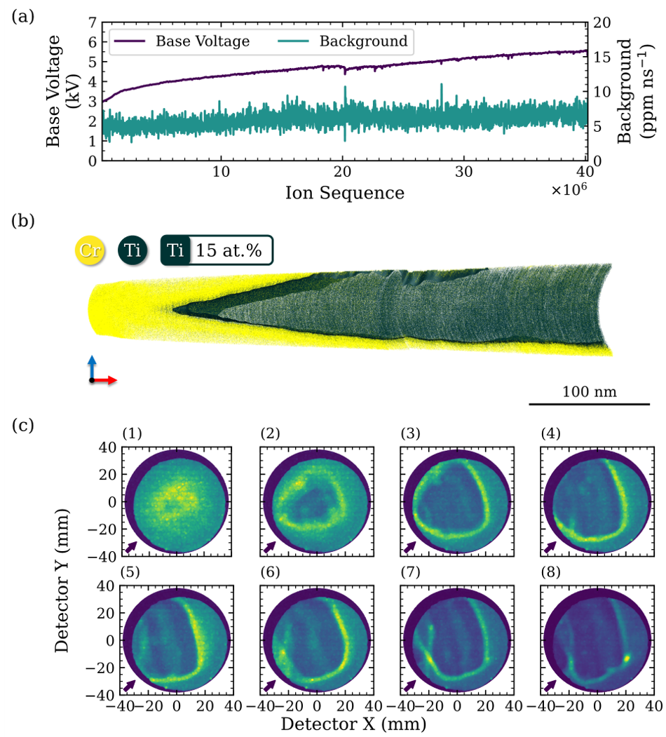
After metallic coating using the in situ sputtering technique, specimens of the free-standing MXene film were successfully analyzed by APT. As visible in the cross-section of the reconstructed 3D atom map in Figure 5 (b), the as-prepared free-standing MXene film specimen is well coated by \ceCr. Some of the \ceCr coating also seems to have penetrated into the stacked material, and has filled nanovoids between the nanosheets. Figure 5 (a) provides a plot of the base voltage and the background level curve of these data, both metrics that indicate how stable the measurement was. Except for small drops, the base voltage steadily and smoothly increases, indicating stable field evaporation conditions. The background is largely constant and below on average. Previous studies have shown that a low and constant background level is essential for the detailed quantification of alkali elements such as \ceLi [46, 31, 16], which can be lost in the background from uncorrelated DC field evaporation due to their low expected evaporation field compared to the other elements composing the material [56].
Compared to previous work, where exfoliated \ceTi3C2T_z MXenes were electrodeposited into \ceCo [22], significantly larger volumes of the material of interest were measured. To illustrate the improvement, the detected \ceTi ion counts, including the contribution of decomposed molecular ions, from the APT data of the exfoliated MXenes from [22] and the free-standing MXenes films were compared. While less than million \ceTi ions were detected in the data set for the exfoliated MXenes embedded in \ceCo, between and million \ceTi ions were collected in the free-standing MXene film in different measurements. All these values refer to data acquired on a 5000XR instrument with a detection efficiency of . Notwithstanding the much simpler and time-saving specimen preparation workflow, the APT data obtained for the nanomaterial is significantly larger and therefore statistically more reliable. In addition, the detector hit maps of the \ceCr coated samples in Figure 5 (c) do not show characteristic hot spots, that would indicate a preferential migration of \ceLi atoms. This confirms that the \ceCr coating prevents the in situ delithiation, as was suggested in previous studies [52].
Besides \ceCr, other materials may also be considered as sputter targets in the future. Although it has been shown that specimens can be easily coated with \ceCr using the in situ sputtering technique, it has some disadvantages for this particular case. During the sputtering process, the clean \ceCr layer is constantly passivated with an oxide layer [47], despite the vacuum inside the SEM-FIB. Since the coating also penetrates into the free-standing film specimen itself to fill nanovoids, the detailed determination of the oxygen content of the nanomaterial becomes nearly impossible. Therefore, \ceCr should be replaced as coating material by a more chemically inert metal in further studies, depending on the adhesion and the probability of peak overlap with the material of interest in the APT mass spectrum.
Conclusion
Despite the great interest in understanding the functional properties of nanomaterials by characterizing their detailed composition, 2D materials have rarely been studied using APT. Using \ceTi3C2T_z MXenes as an example, the common SEM-FIB specimen preparation has been revised utilizing an in situ sputtering technique to facilitate the APT analysis of 2D materials. By processing the colloidal MXene solution into an additive-free free-standing film to enable a common lift-out and sharpening procedure, and by coating the APT specimen, it was possible to acquire relatively large volumes of the 2D material with high data quality. The coating stabilizes the fragile specimen, but also prevents the in situ delithiation of Li, which was incorporated into the material during synthesis. As materials other than MXenes can also be processed into free-standing films [8, 28], the presented workflow has the potential to be a starting point to study the detailed composition of 2D materials with APT.
Acknowledgment
The authors acknowledge financial support from the German Research Foundation (DFG) through DIP Project No. 450800666. The support to the FIB and APT facilities at MPIE by Uwe Tezins, Andreas Sturm and Christian Broß is gratefully acknowledged.
Conflict of Interest
The authors declare no conflict of interest.
Data Availability Statement
The data that support the findings of this study are available from the corresponding authors upon reasonable request.
References
- [1] Vahid R. Adineh, Changxi Zheng, Qianhui Zhang, Ross K.. Marceau, Boyin Liu, Yu Chen, Kae J. Si, Matthew Weyland, Tony Velkov, Wenlong Cheng, Jian Li and Jing Fu “Graphene-Enhanced 3D Chemical Mapping of Biological Specimens at Near-Atomic Resolution” In Advanced Functional Materials 28.32, 2018, pp. 1801439 DOI: 10.1002/adfm.201801439
- [2] Mohamed Alhabeb, Kathleen Maleski, Babak Anasori, Pavel Lelyukh, Leah Clark, Saleesha Sin and Yury Gogotsi “Guidelines for Synthesis and Processing of Two-Dimensional Titanium Carbide (Ti3C2Tx MXene)” In Chemistry of Materials 29.18, 2017, pp. 7633–7644 DOI: 10.1021/acs.chemmater.7b02847
- [3] Babak Anasori, Michael Naguib and Guest Editors “Two-dimensional MXenes” In MRS Bulletin 48.3, 2023, pp. 238–244 DOI: 10.1557/s43577-023-00500-z
- [4] Cédric Barroo, Austin J. Akey and David C. Bell “Aggregated nanoparticles: Sample preparation and analysis by atom probe tomography” In Ultramicroscopy 218, 2020, pp. 113082 DOI: 10.1016/j.ultramic.2020.113082
- [5] Hongwu Chen, Yeye Wen, Yingyi Qi, Qian Zhao, Liangti Qu and Chun Li “Pristine Titanium Carbide MXene Films with Environmentally Stable Conductivity and Superior Mechanical Strength” In Advanced Functional Materials 30.5, 2020, pp. 1906996 DOI: 10.1002/adfm.201906996
- [6] Frédéric De Geuser and Baptiste Gault “Metrology of small particles and solute clusters by atom probe tomography” In Acta Materialia 188, 2020, pp. 406–415 DOI: 10.1016/j.actamat.2020.02.023
- [7] A. Devaraj, M. Gu, R. Colby, P. Yan, C.. Wang, J.. Zheng, J. Xiao, A. Genc, J.. Zhang, I. Belharouak, D. Wang, K. Amine and S. Thevuthasan “Visualizing nanoscale 3D compositional fluctuation of lithium in advanced lithium-ion battery cathodes” In Nature Communications 6.1, 2015, pp. 8014 DOI: 10.1038/ncomms9014
- [8] Dmitriy A. Dikin, Sasha Stankovich, Eric J. Zimney, Richard D. Piner, Geoffrey H.. Dommett, Guennadi Evmenenko, SonBinh T. Nguyen and Rodney S. Ruoff “Preparation and characterization of graphene oxide paper” In Nature 448.7152, 2007, pp. 457–460 DOI: 10.1038/nature06016
- [9] James O Douglas, Michele Conroy, Finn Giuliani and Baptiste Gault “In Situ Sputtering From the Micromanipulator to Enable Cryogenic Preparation of Specimens for Atom Probe Tomography by Focused-Ion Beam” In Microscopy and Microanalysis 29.3, 2023, pp. 1009–1017 DOI: 10.1093/micmic/ozad020
- [10] Sichao Du, Timothy Burgess, Shyeh Tjing Loi, Baptiste Gault, Qiang Gao, Peite Bao, Li Li, Xiangyuan Cui, Wai Kong Yeoh, Hark Hoe Tan, Chennupati Jagadish, Simon P. Ringer and Rongkun Zheng “Full tip imaging in atom probe tomography” In Ultramicroscopy 124, 2013, pp. 96–101 DOI: 10.1016/j.ultramic.2012.08.014
- [11] P. Felfer, T. Li, K. Eder, H. Galinski, A.P. Magyar, D.C. Bell, G.D.W. Smith, N. Kruse, S.P. Ringer and J.M. Cairney “New approaches to nanoparticle sample fabrication for atom probe tomography” In Ultramicroscopy 159, 2015, pp. 413–419 DOI: 10.1016/j.ultramic.2015.04.014
- [12] Baptiste Gault, Ann Chiaramonti, Oana Cojocaru-Mirédin, Patrick Stender, Renelle Dubosq, Christoph Freysoldt, Surendra Kumar Makineni, Tong Li, Michael Moody and Julie M. Cairney “Atom probe tomography” In Nature Reviews Methods Primers 1.1, 2021, pp. 51 DOI: 10.1038/s43586-021-00047-w
- [13] Michael Ghidiu, Maria R. Lukatskaya, Meng-Qiang Zhao, Yury Gogotsi and Michel W. Barsoum “Conductive two-dimensional titanium carbide ‘clay’ with high volumetric capacitance” In Nature 516.7529, 2014, pp. 78–81 DOI: 10.1038/nature13970
- [14] Gerd-Hendrik Greiwe, Zoltan Balogh and Guido Schmitz “Atom probe tomography of lithium-doped network glasses” In Ultramicroscopy 141, 2014, pp. 51–55 DOI: 10.1016/j.ultramic.2014.03.007
- [15] Jan P Josten and Peter J Felfer “Atom Probe Analysis of Nanoparticles Through Pick and Coat Sample Preparation” In Microscopy and Microanalysis 28.4, 2022, pp. 1188–1197 DOI: 10.1017/S1431927621000465
- [16] Se-Ho Kim, Stoichko Antonov, Xuyang Zhou, Leigh T. Stephenson, Chanwon Jung, Ayman A. El-Zoka, Daniel K. Schreiber, Michele Conroy and Baptiste Gault “Atom probe analysis of electrode materials for Li-ion batteries: challenges and ways forward” In Journal of Materials Chemistry A 10, 2022, pp. 4926–4935 DOI: 10.1039/D1TA10050E
- [17] Se-Ho Kim, Phil Woong Kang, O Ok Park, Jae-Bok Seol, Jae-Pyoung Ahn, Ji Yeong Lee and Pyuck-Pa Choi “A new method for mapping the three-dimensional atomic distribution within nanoparticles by atom probe tomography (APT)” In Ultramicroscopy 190, 2018, pp. 30–38 DOI: 10.1016/j.ultramic.2018.04.005
- [18] Se-Ho Kim, Joohyun Lim, Rajib Sahu, Olga Kasian, Leigh T. Stephenson, Christina Scheu and Baptiste Gault “Direct Imaging of Dopant and Impurity Distributions in 2D MoS2” In Advanced Materials 32.8, 2020, pp. 1907235 DOI: 10.1002/adma.201907235
- [19] Se-Ho Kim, Kihyun Shin, Xuyang Zhou, Chanwon Jung, Hyun You Kim, Stella Pedrazzini, Michele Conroy, Graeme Henkelman and Baptiste Gault “Atom probe analysis of BaTiO3 enabled by metallic shielding” In Scripta Materialia 229, 2023, pp. 115370 DOI: 10.1016/j.scriptamat.2023.115370
- [20] Se-Ho Kim, Ayman A. El-Zoka and Baptiste Gault “A Liquid Metal Encapsulation for Analyzing Porous Nanomaterials by Atom Probe Tomography” In Microscopy and Microanalysis 28.4, 2022, pp. 1198–1206 DOI: 10.1017/S1431927621012964
- [21] S. Kölling and W. Vandervorst “Failure mechanisms of silicon-based atom-probe tips” In Ultramicroscopy 109.5, 2009, pp. 486–491 DOI: 10.1016/j.ultramic.2008.11.013
- [22] Mathias Krämer, Bar Favelukis, Ayman A. El-Zoka, Maxim Sokol, Brian A. Rosen, Noam Eliaz, Se-Ho Kim and Baptiste Gault “Near-Atomic Scale Perspective on the Oxidation of Ti3C2Tx MXenes: Insights from Atom Probe Tomography” In Advanced Materials n/a.n/a, pp. 2305183 DOI: 10.1002/adma.202305183
- [23] Changyong Lan, Ziyao Zhou, Renjie Wei and Johnny C. Ho “Two-dimensional perovskite materials: From synthesis to energy-related applications” In Materials Today Energy 11, 2019, pp. 61–82 DOI: 10.1016/j.mtener.2018.10.008
- [24] D.J. Larson, A.D. Giddings, Y. Wu, M.A. Verheijen, T.J. Prosa, F. Roozeboom, K.P. Rice, W.M.M. Kessels, B.P. Geiser and T.F. Kelly “Encapsulation method for atom probe tomography analysis of nanoparticles” In Ultramicroscopy 159, 2015, pp. 420–426 DOI: 10.1016/j.ultramic.2015.02.014
- [25] D.J. Larson, T.J. Prosa, J.H. Bunton, D.P. Olson, D.F. Lawrence, E. Oltman, S.N. Strennin and T.F. Kelly “Improved Mass Resolving Power and Yield in Atom Probe Tomography” In Microscopy and Microanalysis 19.S2, 2013, pp. 994–995 DOI: 10.1017/S143192761300696X
- [26] Tong Li, Arun Devaraj and Norbert Kruse “Atomic-scale characterization of (electro-)catalysts and battery materials by atom probe tomography” In Cell Reports Physical Science 3.12, 2022, pp. 101188 DOI: 10.1016/j.xcrp.2022.101188
- [27] Xiuyan Li and K. Lu “Playing with defects in metals” In Nature Materials 16.7, 2017, pp. 700–701 DOI: 10.1038/nmat4929
- [28] Zhuangnan Li, Ismail Sami, Jieun Yang, Juntao Li, Ramachandran Vasant Kumar and Manish Chhowalla “Lithiated metallic molybdenum disulfide nanosheets for high-performance lithium–sulfur batteries” In Nature Energy 8.1, 2023, pp. 84–93 DOI: 10.1038/s41560-022-01175-7
- [29] Kang Rui Garrick Lim, Mikhail Shekhirev, Brian C. Wyatt, Babak Anasori, Yury Gogotsi and Zhi Wei Seh “Fundamentals of MXene synthesis” In Nature Synthesis 1.8, 2022, pp. 601–614 DOI: 10.1038/s44160-022-00104-6
- [30] Alexey Lipatov, Mohamed Alhabeb, Maria R. Lukatskaya, Alex Boson, Yury Gogotsi and Alexander Sinitskii “Effect of Synthesis on Quality, Electronic Properties and Environmental Stability of Individual Monolayer Ti3C2 MXene Flakes” In Advanced Electronic Materials 2.12, 2016, pp. 1600255 DOI: 10.1002/aelm.201600255
- [31] Xiaonan Lu, Daniel K. Schreiber, James J. Neeway, Joseph V. Ryan and Jincheng Du “Effects of optical dopants and laser wavelength on atom probe tomography analyses of borosilicate glasses” In Journal of the American Ceramic Society 100.10, 2017, pp. 4801–4815 DOI: 10.1111/jace.14987
- [32] Maria R. Lukatskaya, Olha Mashtalir, Chang E. Ren, Yohan Dall’Agnese, Patrick Rozier, Pierre Louis Taberna, Michael Naguib, Patrice Simon, Michel W. Barsoum and Yury Gogotsi “Cation Intercalation and High Volumetric Capacitance of Two-Dimensional Titanium Carbide” In Science 341.6153, 2013, pp. 1502–1505 DOI: 10.1126/science.1241488
- [33] Andrew J. Mannix, Brian Kiraly, Mark C. Hersam and Nathan P. Guisinger “Synthesis and chemistry of elemental 2D materials” In Nature Reviews Chemistry 1.2, 2017, pp. 0014 DOI: 10.1038/s41570-016-0014
- [34] Sajedeh Manzeli, Dmitry Ovchinnikov, Diego Pasquier, Oleg V. Yazyev and Andras Kis “2D transition metal dichalcogenides” In Nature Reviews Materials 2.8, 2017, pp. 17033 DOI: 10.1038/natrevmats.2017.33
- [35] Isabelle Mouton, Tony Printemps, Adeline Grenier, Narciso Gambacorti, Elisa Pinna, Mariavitalia Tiddia, Annalisa Vacca and Guido Mula “Toward an accurate quantification in atom probe tomography reconstruction by correlative electron tomography approach on nanoporous materials” In Ultramicroscopy 182, 2017, pp. 112–117 DOI: 10.1016/j.ultramic.2017.06.007
- [36] Michael Naguib, Murat Kurtoglu, Volker Presser, Jun Lu, Junjie Niu, Min Heon, Lars Hultman, Yury Gogotsi and Michel W. Barsoum “Two-Dimensional Nanocrystals Produced by Exfoliation of Ti3AlC2” In Advanced Materials 23.37, 2011, pp. 4248–4253 DOI: 10.1002/adma.201102306
- [37] Valeria Nicolosi, Manish Chhowalla, Mercouri G. Kanatzidis, Michael S. Strano and Jonathan N. Coleman “Liquid Exfoliation of Layered Materials” In Science 340.6139, 2013, pp. 1226419 DOI: 10.1126/science.1226419
- [38] K.. Novoselov, A.. Geim, S.. Morozov, D. Jiang, Y. Zhang, S.. Dubonos, I.. Grigorieva and A.. Firsov “Electric Field Effect in Atomically Thin Carbon Films” In Science 306.5696, 2004, pp. 666–669 DOI: 10.1126/science.1102896
- [39] Daniel E. Perea, Jonathan E. Allen, Steven J. May, Bruce W. Wessels, David N. Seidman and Lincoln J. Lauhon “Three-Dimensional Nanoscale Composition Mapping of Semiconductor Nanowires” In Nano Letters 6.2, 2006, pp. 181–185 DOI: 10.1021/nl051602p
- [40] Björn Pfeiffer, Torben Erichsen, Eike Epler, Cynthia A Volkert, Piet Trompenaars and Carsten Nowak “Characterization of Nanoporous Materials with Atom Probe Tomography” In Microscopy and Microanalysis 21.3, 2015, pp. 557–563 DOI: 10.1017/S1431927615000501
- [41] Björn Pfeiffer, Johannes Maier, Jonas Arlt and Carsten Nowak “In Situ Atom Probe Deintercalation of Lithium-Manganese-Oxide” In Microscopy and Microanalysis 23.2, 2017, pp. 314–320 DOI: 10.1017/S1431927616012691
- [42] Shi Qiu, Vivek Garg, Shuo Zhang, Yu Chen, Jian Li, Adam Taylor, Ross K.W. Marceau and Jing Fu “Graphene encapsulation enabled high-throughput atom probe tomography of liquid specimens” In Ultramicroscopy 216, 2020, pp. 113036 DOI: 10.1016/j.ultramic.2020.113036
- [43] Shi Qiu, Changxi Zheng, Vivek Garg, Yu Chen, Gediminas Gervinskas, Jian Li, Michelle A. Dunstone, Ross K.. Marceau and Jing Fu “Three-Dimensional Chemical Mapping of a Single Protein in the Hydrated State with Atom Probe Tomography” In Analytical Chemistry 92.7, 2020, pp. 5168–5177 DOI: 10.1021/acs.analchem.9b05668
- [44] Shi Qiu, Changxi Zheng, Qi Zhou, Dashen Dong, Qianqian Shi, Vivek Garg, Wenlong Cheng, Ross K.W. Marceau, Gang Sha and Jing Fu “Direct Imaging of Liquid–Nanoparticle Interfaces with Atom Probe Tomography” In The Journal of Physical Chemistry C 124.35, 2020, pp. 19389–19395 DOI: 10.1021/acs.jpcc.0c05504
- [45] Xiahan Sang, Yu Xie, Ming-Wei Lin, Mohamed Alhabeb, Katherine L. Van Aken, Yury Gogotsi, Paul R.. Kent, Kai Xiao and Raymond R. Unocic “Atomic Defects in Monolayer Titanium Carbide (Ti3C2Tx) MXene” In ACS Nano 10.10, 2016, pp. 9193–9200 DOI: 10.1021/acsnano.6b05240
- [46] Dhamodaran Santhanagopalan, Daniel K. Schreiber, Daniel E. Perea, Richard L. Martens, Yuri Janssen, Peter Khalifah and Ying Shirley Meng “Effects of laser energy and wavelength on the analysis of LiFePO4 using laser assisted atom probe tomography” In Ultramicroscopy 148, 2015, pp. 57–66 DOI: 10.1016/j.ultramic.2014.09.004
- [47] Tim M. Schwarz, Eric Woods, Mahander P. Singh, Chanwon Jung, Leonardo S. Aota, Kyuseon Jang, Mathias Krämer, Se-Ho Kim, Ingrid McCarroll and Baptiste Gault “In-situ metallic coating of atom probe specimen for enhanced yield, performance, and increased field-of-view”, 2023 arXiv:2309.07836 [physics.app-ph]
- [48] Mikhail Shekhirev, Jeffrey Busa, Christopher E. Shuck, Angel Torres, Saman Bagheri, Alexander Sinitskii and Yury Gogotsi “Ultralarge Flakes of Ti3C2Tx MXene via Soft Delamination” In ACS Nano 16.9, 2022, pp. 13695–13703 DOI: 10.1021/acsnano.2c04506
- [49] Mikhail Shekhirev, Christopher E. Shuck, Asia Sarycheva and Yury Gogotsi “Characterization of MXenes at every step, from their precursors to single flakes and assembled films” In Progress in Materials Science 120, 2021, pp. 100757 DOI: 10.1016/j.pmatsci.2020.100757
- [50] Christopher E. Shuck “MXenes are materials, not chemicals: Synthesis factors that influence MXene properties” In MRS Communications, 2023 DOI: 10.1557/s43579-023-00442-2
- [51] Christopher E. Shuck, Asia Sarycheva, Mark Anayee, Ariana Levitt, Yuanzhe Zhu, Simge Uzun, Vitaliy Balitskiy, Veronika Zahorodna, Oleksiy Gogotsi and Yury Gogotsi “Scalable Synthesis of Ti3C2Tx MXene” In Advanced Engineering Materials 22.3, 2020, pp. 1901241 DOI: 10.1002/adem.201901241
- [52] Mahander Pratap Singh, Eric V Woods, Se-Ho Kim, Chanwon Jung, Leonardo S. Aota and Baptiste Gault “Facilitating the systematic nanoscale study of battery materials by atom probe tomography through in-situ metal coating” In Batteries & Supercaps n/a.n/a, pp. e202300403 DOI: 10.1002/batt.202300403
- [53] Karaked Tedsree, Tong Li, Simon Jones, Chun Wong Aaron Chan, Kai Man Kerry Yu, Paul A.. Bagot, Emmanuelle A. Marquis, George D.. Smith and Shik Chi Edman Tsang “Hydrogen production from formic acid decomposition at room temperature using a Ag–Pd core–shell nanocatalyst” In Nature Nanotechnology 6.5, 2011, pp. 302–307 DOI: 10.1038/nnano.2011.42
- [54] Anupma Thakur, Nithin Chandran B.S., Karis Davidson, Annabelle Bedford, Hui Fang, Yooran Im, Vaishnavi Kanduri, Brian C. Wyatt, Srinivasa Kartik Nemani, Valeriia Poliukhova, Ravi Kumar, Zahra Fakhraai and Babak Anasori “Step-by-Step Guide for Synthesis and Delamination of Ti3C2Tx MXene” In Small Methods 7.8, 2023, pp. 2300030 DOI: 10.1002/smtd.202300030
- [55] K. Thompson, D. Lawrence, D.J. Larson, J.D. Olson, T.F. Kelly and B. Gorman “In situ site-specific specimen preparation for atom probe tomography” In Ultramicroscopy 107.2, 2007, pp. 131–139 DOI: 10.1016/j.ultramic.2006.06.008
- [56] T.T. Tsong “Field ion image formation” In Surface Science 70.1, 1978, pp. 211–233 DOI: 10.1016/0039-6028(78)90410-7
- [57] Armin VahidMohammadi, Johanna Rosen and Yury Gogotsi “The world of two-dimensional carbides and nitrides (MXenes)” In Science 372.6547, 2021, pp. eabf1581 DOI: 10.1126/science.abf1581
- [58] Eric V Woods, Mahander P Singh, Se-Ho Kim, Tim M Schwarz, James O Douglas, Ayman A El-Zoka, Finn Giulani and Baptiste Gault “A Versatile and Reproducible Cryo-sample Preparation Methodology for Atom Probe Studies” In Microscopy and Microanalysis, 2023, pp. ozad120 DOI: 10.1093/micmic/ozad120
- [59] Florian Zand, Suzanne J.. Hangx, Christopher J. Spiers, Peter J. Brink, James Burns, Matthew G. Boebinger, Jonathan D. Poplawsky, Matteo Monai and Bert M. Weckhuysen “Elucidating the Structure and Composition of Individual Bimetallic Nanoparticles in Supported Catalysts by Atom Probe Tomography” In Journal of the American Chemical Society 145.31, 2023, pp. 17299–17308 DOI: 10.1021/jacs.3c04474
- [60] Chuanfang (John) Zhang, Lorcan McKeon, Matthias P. Kremer, Sang-Hoon Park, Oskar Ronan, Andrés Seral-Ascaso, Sebastian Barwich, Cormac Ó Coileáin, Niall McEvoy, Hannah C. Nerl, Babak Anasori, Jonathan N. Coleman, Yury Gogotsi and Valeria Nicolosi “Additive-free MXene inks and direct printing of micro-supercapacitors” In Nature Communications 10.1, 2019, pp. 1795 DOI: 10.1038/s41467-019-09398-1
- [61] Jizhen Zhang, Na Kong, Simge Uzun, Ariana Levitt, Shayan Seyedin, Peter A. Lynch, Si Qin, Meikang Han, Wenrong Yang, Jingquan Liu, Xungai Wang, Yury Gogotsi and Joselito M. Razal “Scalable Manufacturing of Free-Standing, Strong Ti3C2Tx MXene Films with Outstanding Conductivity” In Advanced Materials 32.23, 2020, pp. 2001093 DOI: 10.1002/adma.202001093
- [62] A.A. El-Zoka, B. Langelier, G.A. Botton and R.C. Newman “Enhanced analysis of nanoporous gold by atom probe tomography” In Materials Characterization 128, 2017, pp. 269–277 DOI: 10.1016/j.matchar.2017.03.013