Lateral NbS2/MoS2/NbS2 transistors: physical modeling and performance assessment
Abstract
Reducing the contact resistance of field-effect transistors based on two-dimensional materials is one of the key improvements required to to enable the integration of such transistors in an industrially relevant process. Suitably designed lateral heterojunctions provide an opportunity to independently tailor the contact and channel properties and to mitigate the problem of high contact resistance. Inspired by the recent experimental demonstration of a two-dimensional -type Schottky barrier, here we use quantum transport simulations to estimate the performance of -type transistors in which the channel consists of a lateral heterostructure of NbS2/MoS2/NbS2 (semimetal-semiconductor-semimetal). We find that the gate alignment with the channel is a critical design parameter, strongly influencing the capability of the gate to modulate the Schottky barrier at the MoS2/NbS2 interfaces. This effect is also found to significantly affect the scaling behavior of the device.
I Introduction
The possibility of using two-dimensional (2D) materials in an industrially relevant CMOS process depends on a few factors, among which the capability to fabricate low-resistance metal contacts is critical. Unfortunately, 2D semiconductors tend to form high Schottky barriers with bulk metals, and the difficulty in achieving high doping levels in monolayers hinders the adoption of the conventional approach based on thinning these barriers enough to make them transparent to carrier tunnelling Tersoff (1984); Yang et al. (2014); Allain et al. (2015).
Contacting semiconducting monolayers by defining vertical or lateral heterojunctions with 2D material-based metals has been attracting significant interest Jena et al. (2014); Kaushik et al. (2016); Xie et al. (2017); Schulman et al. (2018); Cai et al. (2022); Chen et al. (2022); Choi et al. (2022); Schneider et al. (2021), especially in the perspective of developing all-2D circuits where every circuit component, including metallizations and insulating regions, is based on 2D materials.
In vertical heterojunctions, monolayers are weakly coupled by van der Waals interactions. This prevents the undesired occurrence of interfacial spurious states and Fermi level pinning Tersoff (1984); Kim et al. (2017); Wang et al. (2019); Liu et al. (2022); however, the small coupling also entails low carrier injection Wang et al. (2019). On the other hand, the edge contact between monolayers in lateral heterojunctions is characterized by a stronger coupling due to the covalent character of the atomic bonds. Provided that the quality of the interface is controlled and the height of the Schottky barrier is low enough, this translates to potentially efficient carrier injection Zhang et al. (2018); Shen et al. (2021).
The capability to engineer both - and -type contacts is another essential requirement to implement a CMOS technology. Unfortunately, realizing -type FETs based on 2D materials has proven extremely challenging, due to the strong influence of the commonly used dielectric substrates, that tend to induce an -type doping in the channel and of Fermi level pinning at the conduction band He et al. (2019). In this respect, recent experiments have demonstrated the fabrication of -type Schottky diodes based on a lateral heterojunction of NbS2 and MoS2 Wang et al. (2023). The reported, significant, current modulation indicates an effective reduction of the parasitic resistance associated to the MoS2 contact when the NbS2 buffer region is included. Considering some critical parameters extracted from Ref. Wang et al. (2023) and by means of quantum transport simulations, in this paper we study the physics and the upper performance limit of a -type field-effect transistor based on a monolayer MoS2 channel connected to monolayer NbS2 access regions through lateral heterojunctions. Our results indicate that the phonon-assisted interband tunnelling at the NbS2/MoS2 interfaces plays a major role in determining the device behavior. It also translates into a pronounced sensitivity of the device to some architectural details, such as the alignment between the gate electrode and the channel, that should be carefully addressed in order to optimize its performance.
The paper is organized as follows. In Section II, we present our model and simulation strategy. In Section III, we discuss our results in terms of the device physics, performance and optimization opportunities. Our concluding remarks are drawn in Section IV.
II Model
Following Ref. Wang et al. (2023), we model the isolated monolayers by means of the two-bands first-nearest neighbor tight-binding Hamiltonian
| (1) |
where (MoS2, NbS2), for MoS2, is the energy gap and is the maximum energy of the valence band, while the minimum of the NbS2 band that couples with it is given by . Moreover, is the hopping parameter and
| (2) |
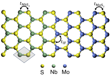
is the Bloch function describing the periodicity of the hexagonal lattice. In agreement with the experimental and theoretical analyses in Wang et al. (2023), the MoS2-NbS2 band alignment was set in order to fulfill the constraint =, where is the electrochemical potential at the NbS2 contacts. The interface between the monolayers is assumed defectless (see Fig. 1) and the hopping between NbS2 sulphur atoms and MoS2 molybdenum atoms is assumed equal to . Due to the closeness between the values of and , no significant differences are expected by setting to or to an intermediate value between and . We report the parameters of the model in Table 1.
Transport simulations were performed within the non-equilibrium Green’s function formalism Datta (2002). An orthorhombic elementary cell is designated to describe the system in real space in the direction of transport, and the device is assumed periodic in the lateral direction orthogonal to it. To sample the Brillouin zone along this transverse direction, a set of 100 transverse wave vectors were taken into account in simulations. In order to obtain a self-consistent solution, the transport equations were nonlinearly coupled with the 2D Poisson equation in the device cross section. The resulting system of equations was iteratively solved by adopting a fixed-point approach. Convergence was considered achieved when the maximum difference between the potential energy profile in consecutive iterations was less than 1 meV.
Electron-phonon scattering was included in the transport equations within the self-consistent Born approximation through diagonal self-energies Lee et al. (2009) and by assuming an elastic and dispersionless approximation for acoustic and optical phonons, respectively. The optical phonon energy was obtained as the arithmetical average of the longitudinal, transverse and homopolar optical branches in MoS2, and set to meV Li et al. (2013). Hole-phonon coupling was modeled within the deformation potential approximation, by only considering the intravalley hole scattering at the point Jin et al. (2014). The values of the acoustic and optical deformation potentials ( and , respectively) are reported in Table 1.

III Results and discussion
The cross-section of the NbS2/MoS2/NbS2 transistor is sketched in Fig. 2. The current flow is controlled by means of a top and a bottom gate, separated from the channel by a -thick HfO2 layer with relative permittivity . The gate length can be larger or smaller than the MoS2 channel length ; this difference is quantified by the algebraic parameter . The NbS2 source (S) and drain (D) extensions are long. According to the estimates in Ref. Wang et al. (2023), the MoS2 channel is p-doped at a concentration .
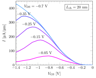
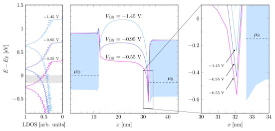
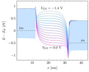
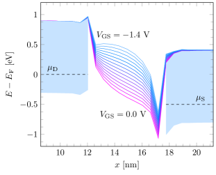
Fig. 3(a) illustrates the transfer characteristics of the transistor for nm, and different values of . A pronounced maximum of the current is observed, that shifts towards more negative as increases. This effect can be explained with the help of Fig. 3(b), that reports the band diagram of the transistor (central panel) for V and three values of , located before, at, and after the current peak. The corresponding local density of states (LDOS) in the middle of the channel is shown in the left panel of the figure, while the right panel presents a magnified view of the band diagram close to the MoS2/NbS2 interface at the source. The LDOS exhibits a peak, corresponding to the local flattening of the MoS2 valence band at the point. The current is mainly limited by two factors: the density of available states in the channel between the source and drain electrochemical potentials (grey stripe in Fig. 3(b)), and the width of the tunneling barrier at the channel-drain interface. As the gate voltage is swept through the current peak, the barrier thins, while the density of states decreases. The competition between the two phenomena induces the current peak.
When the absolute value of increases, the tunneling barrier at the source/channel interface at a given energy widens. As a consequence, more negative gate voltages are needed to reach the current peak.
At V and V, the ratio equals 2330 and 1290, respectively. These value are obtained by setting IRD (2021) and computing at , where is the gate voltage at which . We maintain these definitions through the paper.
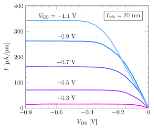
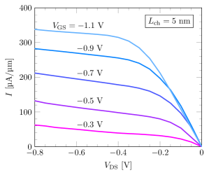
The output characteristics of the transistor with nm are reported in Fig. 3(c). An excellent current saturation at large bias is observed. Furthermore, we can observe that at low the curve at V intersects with the curve at lower . This is simply due to the presence of the peak in the characteristics showed in Figure 3(b). Fig. 3(d) shows the band diagram along the device for several values of , which confirms an almost perfect electrostatic control of the gate over the channel potential, corresponding to a gate efficiency , where is the top of the valence band at the center of the channel.
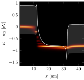
Despite this almost ideal electrostatic control of the gate over the channel, the subthreshold swing of the device is about and is thus degraded with respect to the thermionic limit of . This is a direct consequence of the carrier energy relaxation due to phonon emission, which allows the interband electron transmission at the channel-drain interface also when the the top of the valence band in the middle of the channel is pushed below the lower edge of the NbS2 band. This effect is illustrated in Fig. 3(e), which reports the current spectral density when the device operates in the subthreshold region.
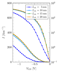
In Fig. 4(a) we explore the scaling behavior of the transistor. Transfer characteristics are almost overlapping for nm, while significant performance degradation are observed for nm. Particularly, the subthreshold swing increases to mV/dec and the ratio correspondingly drops to 740 and 300 for V and V, respectively (see Table 2). Also, the output resistance undergoes a large decrease, settling to km at V (see Fig. 4(b)). The performance drop can be traced back to a strongly reduced capability of the gates to modulate the channel potential, as illustrated in panel Fig. 4(c). Quantitatively, for nm the gate efficiency reduces to . Another marker of performance degradation as the channel length shrinks, is the threshold voltage roll-off with respect to the nm case, which is reported in Table 3 for the other considered values of .
| [V] | [nm] | |
|---|---|---|
| 5 | 300 | |
| 10 | 1180 | |
| 15 | 1280 | |
| 20 | 1290 | |
| 5 | 740 | |
| 10 | 2130 | |
| 15 | 2300 | |
| 20 | 2330 |
| [] | [] | [] |
|---|---|---|
| @ | @ | |
| 5 | 0.16 | 0.25 |
| 10 | 0.02 | 0.05 |
| 15 | 0.01 | 0.03 |
The effect of gate overlaps and underlaps on the ratio for nm is reported in Table 4. As one expects, the presence of overlaps has the effect of improving the ratio, as it results in a better electrostatic control over the channel potential. On the contrary, the presence of underlaps is detrimental to the device performance. More importantly, a comparison between Table 2 and Table 4 highlights that the impact of the gate overlap (underlap) is much stronger than an equivalent gate extension (reduction) with . For instance, an increase of from 10 nm to 15 nm by symmetrically including 2.5 nm-long overlaps on the source and drain sides, results in a 30% improvement of the ratio, while an equivalent extension of with only results in a 8% improvement. Analogously, a decrease of from 15 nm to 10 nm by symmetrically including 2.5 nm-long underlaps on the source and drain sides degrades the ratio by 48%, while an equivalent gate shrinking with only yields a 8% reduction. This is a consequence of the modulating effect of the gate over the Schottky barrier thickness already highlighted in Fig. 3(b). When decreases, more holes are induced in the MoS2 channel, leading to a reduction in the size of the depletion regions associated with the Schottky barriers; this results in a thinning effect on the barriers themselves. In the presence of gate overlaps, the gate is more effective in inducing charge close the NbS2/MoS2 interfaces and therefore in thinning the barriers and modulating the current.
| [V] | [nm] | |
|---|---|---|
| 0.6 | 2.5 | 670 |
| 0.6 | 0.0 | 1280 |
| 0.6 | 2.5 | 1540 |
| 0.8 | 2.5 | 1299 |
| 0.8 | 0.0 | 2300 |
| 0.8 | 2.5 | 2630 |
Finally, in order to comprehensively evaluate the potential of the device, we analyze several dynamic performance metrics that are relevant to a wide range of technological applications. These metrics include the intrinsic delay time (), the power-delay product () and the cut-off frequency (). The intrinsic delay time and power-delay product are the basic figures of merit in digital applications, while the cut-off frequency characterizes the device with respect to radiofrequency applications.
and are calculated in a quasi-static approximation using the equations Mazziotti et al. (2022)
| (3) |
| (4) |
where and are the total charge in the channel in the ON and OFF states, respectively. The cut-off frequency is evaluated as Mazziotti et al. (2022)
| (5) |
where is the total capacitance seen from the gates and is the transistor transconductance. The results are shown in Fig. 5 as a function of the channel length .
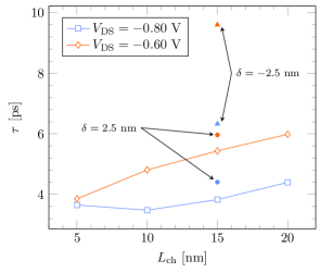
The intrinsic delay time as a function of is shown in Fig. 5(a).
For nm and , the intrinsic delay time decreases approximately linearly with .
Larger deviations from this behavior are observed for nm, as the values of for and V approximately converge toward a common value of 3.8 ps.
The dependence on is quantified for nm. A large increase of with respect to the case is observed for , due to the previously discussed degradation.
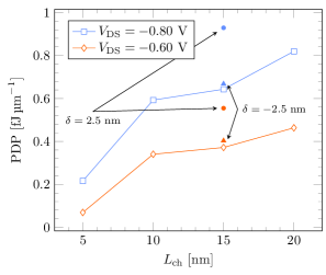
The power-delay product showed in Fig. 5(b) increases with increasing and , according to Equation 4.
A significant increase is observed in the presence of gate overlaps, which indirectly causes an increases of by enhancing the coupling between the channel and the contacts.
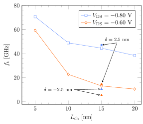
At fixed , the cutoff frequency showed in Fig. 5(c) follows a behavior. Increasing entails an increase of and, in turn, an increase of . In the presence of gate underlaps, the dependence of the transconductance on becomes much weaker and tends to settle to a common value of GHz.
IV Conclusions
The possibility to fabricate -type field-effect transistors based on 2D materials is essential to develop a CMOS process based on 2D materials. Following recent experimental demonstrations, we have modeled and numerically simulated a p-type transistor based on lateral heterojunctions of MoS2 and NbS2 monolayers. The metallic NbS2 regions act as source and drain extensions, mediating between the MoS2 channel and the 3D metal contacts of source and drain. Our results indicate that the performance of the device is strongly dependent on the modulation of the Schottky barriers at the MoS2/NbS2 interfaces as a function of both the gate voltage and the drain-to-source bias. In this respect, the gate length and the gate alignment with the MoS2/NbS2 interfaces prove to be critical parameters to optimize the device performance. These geometrical considerations are expected to have a broader applicability and to describe some general tradeoffs in the design of lateral heterojunction field-effect transistors based on two-dimensional materials. The scaling behavior shows a strong reduction of the / ratio at channel lengths of 5 nm, while the dynamic figures of merit remain dominated by capacitive effects and generally improve as the channel shrinks.
V Acknowledgements
This work was partially supported by the European Union Horizon 2020 Framework Programme under the “Quantum Engineering for Machine Learning” (QUEFORMAL) project (Grant Agreement No. 829035), by the by the Italian MIUR through the PRIN project FIVE2D and by the Italian Ministry of University and Research through the ForeLab Departments of Excellence Grant
References
- Tersoff (1984) J. Tersoff, Phys. Rev. Lett. 52, 465 (1984).
- Yang et al. (2014) L. Yang, K. Majumdar, H. Liu, Y. Du, H. Wu, M. Hatzistergos, P. Y. Hung, R. Tieckelmann, W. Tsai, C. Hobbs, and P. D. Ye, Nano Letters 14, 6275 (2014), pMID: 25310177, https://doi.org/10.1021/nl502603d .
- Allain et al. (2015) A. Allain, J. Kang, K. Banerjee, and A. Kis, Nature Materials 14, 1195 (2015).
- Jena et al. (2014) D. Jena, K. Banerjee, and G. H. Xing, Nature Materials 13, 1076 (2014).
- Kaushik et al. (2016) N. Kaushik, D. Karmakar, A. Nipane, S. Karande, and S. Lodha, ACS Applied Materials & Interfaces 8, 256 (2016), pMID: 26649572, https://doi.org/10.1021/acsami.5b08559 .
- Xie et al. (2017) L. Xie, M. Liao, S. Wang, H. Yu, L. Du, J. Tang, J. Zhao, J. Zhang, P. Chen, X. Lu, G. Wang, G. Xie, R. Yang, D. Shi, and G. Zhang, Advanced Materials 29, 1702522 (2017), https://onlinelibrary.wiley.com/doi/pdf/10.1002/adma.201702522 .
- Schulman et al. (2018) D. S. Schulman, A. J. Arnold, and S. Das, Chem. Soc. Rev. 47, 3037 (2018).
- Cai et al. (2022) X. Cai, Z. Wu, X. Han, Y. Chen, S. Xu, J. Lin, T. Han, P. He, X. Feng, L. An, R. Shi, J. Wang, Z. Ying, Y. Cai, M. Hua, J. Liu, D. Pan, C. Cheng, and N. Wang, Nature Communications 13, 1777 (2022).
- Chen et al. (2022) S. Chen, S. Wang, C. Wang, Z. Wang, and Q. Liu, Nano Today 42, 101372 (2022).
- Choi et al. (2022) M. S. Choi, N. Ali, T. D. Ngo, H. Choi, B. Oh, H. Yang, and W. J. Yoo, Advanced Materials 34, 2202408 (2022), https://onlinelibrary.wiley.com/doi/pdf/10.1002/adma.202202408 .
- Schneider et al. (2021) D. S. Schneider, E. Reato, L. Lucchesi, Z. Wang, A. Piacetini, J. Bolten, D. Marian, E. G. Marin, A. Radenovic, Z. Wang, G. Fiori, A. Kis, G. Iannaccone, D. Neumaier, and M. C. Lemme, in 2021 Device Research Conference (DRC) (2021) pp. 1–2.
- Kim et al. (2017) C. Kim, I. Moon, D. Lee, M. S. Choi, F. Ahmed, S. Nam, Y. Cho, H.-J. Shin, S. Park, and W. J. Yoo, ACS Nano 11, 1588 (2017), pMID: 28088846, https://doi.org/10.1021/acsnano.6b07159 .
- Wang et al. (2019) Y. Wang, J. C. Kim, R. J. Wu, J. Martinez, X. Song, J. Yang, F. Zhao, A. Mkhoyan, H. Y. Jeong, and M. Chhowalla, Nature 568, 70 (2019).
- Liu et al. (2022) X. Liu, M. S. Choi, E. Hwang, W. J. Yoo, and J. Sun, Advanced Materials 34, 2108425 (2022), https://onlinelibrary.wiley.com/doi/pdf/10.1002/adma.202108425 .
- Zhang et al. (2018) Y. Zhang, L. Yin, J. Chu, T. A. Shifa, J. Xia, F. Wang, Y. Wen, X. Zhan, Z. Wang, and J. He, Advanced Materials 30, 1803665 (2018), https://onlinelibrary.wiley.com/doi/pdf/10.1002/adma.201803665 .
- Shen et al. (2021) P.-C. Shen, C. Su, Y. Lin, A.-S. Chou, C.-C. Cheng, J.-H. Park, M.-H. Chiu, A.-Y. Lu, H.-L. Tang, M. M. Tavakoli, G. Pitner, X. Ji, Z. Cai, N. Mao, J. Wang, V. Tung, J. Li, J. Bokor, A. Zettl, C.-I. Wu, T. Palacios, L.-J. Li, and J. Kong, Nature 593, 211 (2021).
- He et al. (2019) Q. He, Y. Liu, C. Tan, W. Zhai, G.-h. Nam, and H. Zhang, ACS Nano 13, 12294 (2019), publisher: American Chemical Society.
- Wang et al. (2023) Z. Wang, M. Tripathi, Z. Golsanamlou, P. Kumari, G. Lovarelli, F. Mazziotti, D. Logoteta, G. Fiori, L. Sementa, G. M. Marega, H. G. Ji, Y. Zhao, A. Radenovic, G. Iannaccone, A. Fortunelli, and A. Kis, Advanced Materials 35, 2209371 (2023).
- Datta (2002) S. Datta, in Digest. International Electron Devices Meeting, (2002) pp. 703–706.
- Lee et al. (2009) W. Lee, N. Jean, and S. Sanvito, Phys. Rev. B 79, 085120 (2009).
- Li et al. (2013) X. Li, J. T. Mullen, Z. Jin, K. M. Borysenko, M. Buongiorno Nardelli, and K. W. Kim, Phys. Rev. B 87, 115418 (2013).
- Jin et al. (2014) Z. Jin, X. Li, J. T. Mullen, and K. W. Kim, Phys. Rev. B 90, 045422 (2014).
- IRD (2021) “More moore tables. international roadmap for devices and systems (irds),” https://irds.ieee.org/editions/2021 (2021), accessed: 2023-10-04.
- Mazziotti et al. (2022) F. Mazziotti, D. Logoteta, and G. Iannaccone, Phys. Rev. Appl. 17, 014011 (2022).