Avoided metallicity in a hole-doped Mott insulator on a triangular lattice
Abstract
Charge carrier doping of a Mott insulator is known to give rise to a wide variety of exotic emergent states, from high-temperature superconductivity to various charge, spin, and orbital orders. The physics underpinning their evolution is, however, poorly understood. A major challenge is the chemical complexity associated with traditional routes to the addition or removal of carriers. Here, we study the Mott insulating CrO2 layer of the delafossite oxide PdCrO2, where an intrinsic polar catastrophe provides a clean route to induce substantial doping of the surface layer. Despite this, from scanning tunneling microscopy and angle-resolved photoemission, we find that the surface retains an insulating character, but with a modified electronic structure and the development of a short-range ordered state with a distinct periodicity. From density functional theory, we demonstrate how this reflects the formation of an intricate charge disproportionation that results in an insulating ground state of the surface layer that is disparate from the hidden Mott insulator found in the bulk. By applying voltage pulses to the surface layer, we induce substantial local modifications to this state, which we find relax on a time scale of tens of minutes, pointing to a glassy nature of the charge-disproportionated insulator realised here.
Introduction
The Mott-Hubbard Hamiltonian is one of the simplest models to describe correlated electron physics, capturing phenomena ranging from antiferromagnetic order in a Mott insulator to potentially explaining the high temperature superconductivity in cuprates. It yields particularly exciting predictions for systems on triangular lattices, including, for a single-orbital Hubbard model, the famed resonating valence bond state 1 and the formation of quantum spin liquids and complex magnetic orders2. In multi-orbital systems, the situation is even richer: for example for transition metal atoms with a partially filled manifold, the interplay of spin-orbit coupling with correlations can result in topologically non-trivial fractional Chern states,3; 4 while charge carrier doping can lead to exotic superconducting states5. This large variety of unconventional ground states motivates the study of triangular-lattice Mott systems experimentally, and in particular probing the evolution of their ground states with doping.
Here, we establish the surface of PdCrO2 as a model system in which to investigate the competing ground states of a doped triangular-lattice Mott system. Its bulk crystal structure (Fig. 1a) consists of stacked triangular-lattice Pd1+ and (CrO2)1- layers. The former are in a charge state, forming highly conductive metallic layers 6; 7; 8; 9. In contrast, the latter host Cr3+ ions, with a electron configuration which half-fills the manifold. These layers are Mott insulating, and develop an antiferromagnetic (AF) order below a Néel temperature of K 10; 11; 12; 8. This naturally occurring heterostructure of metallic and Mott-insulating layers makes this “hidden” Mott state 12 an ideal candidate for detailed spectroscopic study 8.
The alternating / nominal valences of the \cePd and \ceCrO2 layers reflect a net charge transfer of one electron from Pd to the neighbouring \ceCrO2 layers in the bulk (cf. Fig. 1a). The loss of such charge transfer processes at the surface, however, is expected – in a simple ionic picture – to result in an approximately 0.5 holes/Cr (0.5 electrons/Pd) self-doping of the \ceCrO2 (\cePd) terminated surface. Such electronic reconstructions – akin to models for the \ceSrTiO3/\ceLaAlO3 interfacial electron gas 13 – have already been observed for the \ceCoO2-based delafossites, resulting in the stabilisation of Rashba-coupled and ferromagnetic metallic surface states on the \ceCoO2 and \cePd terminated surfaces, respectively 14; 15; 16; 17; 18. For the \ceCrO2-terminated surface of \cePdCrO2, the same mechanism would naively be expected to mediate a substantial doping of 0.5 holes/Cr of the Mott insulating state found in the bulk, and drive an insulator-metal transition. In contrast, we show here that the doping triggers a charge-disproportionation in the surface layer, inducing a structural corrugation distinct to the bulk, and driving the surface layer insulating. We further demonstrate that the charge disproportionated state exhibits short range order and glassy dynamics, evidencing a high degree of degeneracy of the ground state.

Results and Discussions
.1 Surface Determination
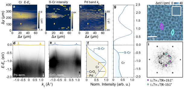
Due to the stronger bonding between \ceCr and \ceO within the \ceCrO2 octahedra as compared to the bond between oxygen and palladium atoms, \cePdCrO2 is expected to cleave between \cePd and \ceO. This results in two surface terminations that leave the in-plane order intact – a \cePd and a \ceCrO2 terminated one (Fig. 1a). Consistent with this simple picture, we show in Fig. 1b a topographic scanning tunneling microscopy (STM, see Methods) image of the surface of a freshly cleaved sample. The region comprises two flat terraces separated by a step edge. The step height is only , less than the expected for adjacent terraces of identical surface termination. This, as well as the different corrugations of the surfaces, suggests that the step edge here is between surfaces of distinct atomic characters. Similarly, the presence of two different surface terminations is also evidenced by our spatially-resolved photoemission measurements, performed using a light spot of m in lateral size (see Methods). We show in Fig. 1c the spatial variations of the binding energy of the Cr 3 core level, imaged over a region of of the cleaved surface. Characteristic core-level shifts of are observed, varying between patches of the sample with lateral sizes of m. The extracted core level spectra integrated over the regions shown in Fig. 1c are shown in Fig. 1d, spanning both the Cr 3 and Pd 4 core levels. The spectrum which exhibits the higher binding energy of the \ceCr 3 core level (region B, orange line) also exhibits a much more substantial \cePd 4 peak, which is almost completely absent in the spectrum from region A (blue line), similar to termination-dependent core-level spectra from the related material \ceAgCrSe2 19. In our atomically-resolved STM data, curves (bottom-left inset of Fig. 1b) likewise show different apparent barrier heights. We thus assign the surface regions characterized by a higher binding energy of the \ceCr 3 core-level and lower apparent barrier height as \cePd-terminated surface regions, and those exhibiting a lower binding energy of the \ceCr 3 peak and larger apparent barrier height as \ceCrO2-terminated areas.
.2 Near-Fermi level electronic structure of the CrO2-terminated surface
The reduced binding energy of the \ceCr 3 core-level for the \ceCrO2-terminated surface already provides spectroscopic evidence for the expected hole doping of the surface \ceCrO2 layer introduced above. To probe the influence of this on the low-energy electronic structure, we show in Fig. 2a-f spatial- and angle-resolved photoemission measurements performed over the same spatial region as the core-level mapping in Fig. 1c. Fig. 2d and e show the measured electronic dispersion of a Pd and CrO2 terminated region, respectively, as identified from our core level mapping in Fig. 1c (see yellow and blue markers in Fig. 2a-c for the measurement position). In both regions, we find highly-dispersive bands derived from the bulk-like Pd states 6; 7; 8, which cross the Fermi level () at a Fermi wave vector Å-1. From fitting of momentum distribution curves (MDCs) at , we find a small but non-negligible decrease of for the \ceCrO2- versus the \cePd-terminated surface regions (Fig. 2c), indicating a weak hole doping of these \cePd-derived states for the \ceCrO2-terminated surface.
In addition to these metallic states, we observe rather diffuse spectral weight gapped away from , which varies much more significantly between the two surface terminations. We attribute this spectral weight to states of Cr-derived character. For the Pd-terminated regions, this diffuse weight is peaked at a binding energy of eV (evident in the -integrated spectrum in Fig. 2f), consistent with the location of the lower Hubbard band which derives from the bulk \ceCrO2 Mott insulating layer 8. For the \ceCrO2-terminated surface, however, we find that this component shifts towards lower binding energies by around , while a pronounced shoulder (S-Cr in Fig. 2f) develops closer to the Fermi level at . All of these spectral features – the shift to lower binding energy of the dominant Cr-derived density of states (DOS) peak (Fig. 2a), development of spectral weight of the lower-energy shoulder (S-Cr, Fig. 2b), and decrease in of the Pd-derived band (Fig. 2c) – show a spatial dependence that is closely correlated with our identification of \ceCrO2-derived regions from our core-level spatial mapping (Fig. 1c), indicating that they are characteristic signatures of the electronic structure of the \ceCrO2-terminated surface.
A direct comparison to our tunneling spectra measured on the \ceCrO2-terminated surface, shown in Fig. 2g, reveals similar features. The differential conductance spectrum shows a clear gap-like structure, with gap edges at , vanishingly small DOS inside the gap, and an onset of tunneling into the occupied states and a broad maximum that are in good agreement with the S-Cr feature observed in ARPES. Taken together, our surface-sensitive spectroscopic measurements thus demonstrate clear modifications in the electronic structure of the \ceCrO2-terminated surface from that of the Mott-insulating \ceCrO2 layers of the bulk. Nonetheless, despite the large doping away from half-filling which is inherent to this polar surface, our measurements show that it remains insulating, defying the simple expectation for such a heavily doped Mott insulator. This suggests that a different form of correlated insulating state is obtained here.
While the differential conductance measured by STM inside the surface gap becomes almost zero, tunneling through the surface layer to the Pd layer underneath remains possible, although it requires extremely small tunneling currents (below ) to achieve stable tunneling. Excitingly, this enables detailed probing of the correlated states of the surface layer, which would otherwise be extremely challenging for such an insulating layer. Atomically resolved STM measurements performed at a bias voltage of , outside the gap, show an unreconstructed, perfect triangular lattice with a unit cell (inset in Fig. 1b). We find a notable change in the appearance of this surface topography, however, when imaging the surface at energies inside the gap (Fig. 2h). An additional contrast to that of the regular \ceCr lattice is evident, which appears rather disordered. The point defects, clearly visible in the topography in Fig. 1b, become virtually invisible when imaged at low energies (see Suppl. Note 2, Suppl. Fig. 2). From the real-space image and its Fourier transform (Fig. 2i), we can identify a characteristic length scale, indicating the formation of a short-range ordered state. From the dominant features in the Fourier transform, we identify the basic building block of this short-range order as a unit.
.3 Formation of a charge disproportionated insulator
To understand why the surface layer remains insulating, despite the significant charge transfer, and the origins of its peculiar local order, we have modelled a \cePdCrO2 slab and performed spin-polarized Density Functional Theory (DFT) calculations. We use a DFT+U scheme to include the effect of correlations – a calculation scheme which we find well reproduces the hidden Mott gap of the bulk electronic structure, Fig. 3a (see Suppl. Note 3 for details).
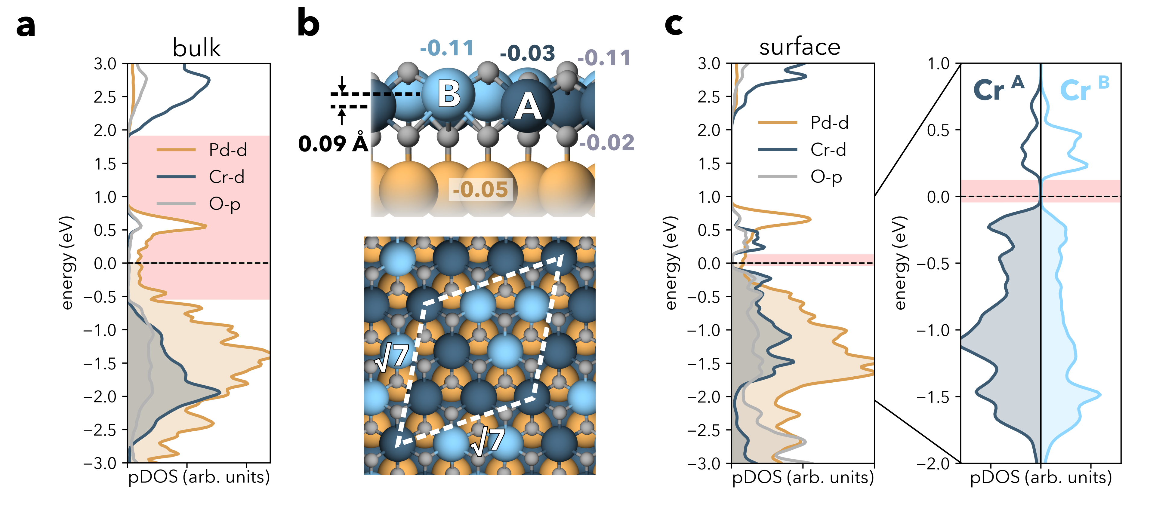
We have modelled the \ceCrO2 surface by a slab containing three Pd and four \ceCrO2 layers in a unit cell enclosed by vacuum. Calculations using such a slab, including relaxation, stabilize a ferromagnetic ground state in the surface \ceCrO2 layer that is metallic – as expected for a heavily-doped Mott insulator, but clearly inconsistent with our spectroscopic data. To address this discrepancy, we introduce the peculiar order observed in our STM measurements into the calculations by creating a unit cell containing seven Cr atoms per layer. Relaxing the atomic positions in this unit cell results in a structural modification of the surface layer which leads to two distinct types of Cr atoms, CrA and CrB, which are distributed with a 4:3 ratio and arranged in a pattern as depicted in Fig. 3b.
Cr atoms of both types relax outwards at the surface, but by different amounts. The relaxation results in an off-centring of the Cr atoms within the surface CrO6 octahedra, by and for CrA and CrB atoms, respectively, with the larger out-of-plane relaxation of CrB accompanied by a larger distortion of the octahedra. The difference of in the height of the two Cr species provides a natural explanation for the contrast in the STM images evident in Fig. 2h.
Most strikingly, this structural distortion renders the surface insulating, stabilizing a full gap of within the Cr manifold, as depicted in Fig. 3c. In agreement with our STM and ARPES measurements, this gap is substantially smaller when compared to the bulk gap which separates the and manifolds. This is in stark contrast with calculations for an unreconstructed surface, where DFT calculations yield a metallic state (see Suppl. Note 4).
The key question is therefore why the \ceCrO2 surface avoids such a metallic state and how the insulating state results in the reconstructed surface layer. In a purely ionic picture (Fig. 1a), simple electron counting would suggest that the 0.5 hole/Cr doping of the surface layer could be accommodated via a charge ordering of the Cr sites, with equal numbers of and occupancies to give an average configuration. In line with this picture, we find that the charges in the surface \ceCrO2 layer redistribute laterally, resulting in CrA atoms containing more electrons in their manifold than CrB atoms (upper panel in Fig. 3b). This is reflected by a higher magnetic moment of the CrA sites of 2.83 (close to the 2.89 of the bulk) as compared to 2.49 of the CrB atoms. A Bader charge analysis provides additional support for such a picture, with CrA (CrB) atoms having 0.03 (0.11) fewer electrons than the Cr atoms in the bulk (Fig. 3b).
Our analysis, however, indicates that the additional surface charge is not purely accommodated by the surface Cr atoms. The topmost oxygen atoms, sitting above the Cr layer, have fewer electrons than those in the bulk (Fig. 3b). Furthermore, the doping is not confined exclusively to the surface \ceCrO2 layer, and we find a slight hole doping (0.05 holes/Pd) for the subsurface Pd layer, as evidenced by a shift of its \cePd band crossing by towards lower binding energies compared to the \cePd bands in deeper layers (see Suppl. Note 5, Suppl. Fig. 7a, b). In consequence, there are less than 0.5 holes/Cr left to be distributed among the Cr atoms and slightly more than half of the Cr atoms (CrA) stay in a bulk-like configuration (as inferred from their magnetic moment), while the remainder of the Cr atoms (CrB) end up in a configuration as close as possible to . This charge disproportionation lowers the energy when compared to a metallic state, where charges are delocalized and homogeneously distributed among the atoms of the same species.
The charge disproportionation and the accompanying structural modification are thus instrumental in avoiding metallicity and maintaining the insulating nature of the surface \ceCrO2 layer. Also, we find that details of the magnetic order on the Cr atoms only affect the size of the gap, but not its presence, hence suggesting that charge disproportionation is the primary driver for the insulating ground state (see Suppl. Note 4, Suppl. Fig. 6).
.4 Glassy dynamics
While our calculations and experiments demonstrate that the doped Mott layer at the surface of PdCrO2 forms a charge disproportionated insulator, both, data and experiments, also point towards a competition of ground states with similar periodicity. In the experiments, this is evidenced by the short-ranged nature of the order suggesting that it is frustrated and only presents a shallow energy minimum, while in calculations a number of different magnetic ground states are close by in energy. In STM images, the structural modification can only be imaged at extremely small tunneling currents (Fig. 2h), whereas using higher currents triggers changes in the order and STM images appear fuzzy (see Suppl. Note 6, Suppl. Fig. 8, also Suppl. Fig. 2), suggesting that the ground state is susceptible to small perturbations.
Moreover, we find that changes in the surface order can be triggered through deliberate voltage pulses, disrupting the short range order as seen through changes in the topographic appearance imaged at very low tunneling currents. The system slowly relaxes towards a new equilibrium, enabling us to study the resulting temporal dynamics of the system. Fig. 4 shows such a measurement series. In Fig. 4a, we show the appearance of the short-range order of the surface layer before applying a voltage pulse in the centre of the image. Figs. 4(b–d) show the time evolution after the voltage pulse has been applied. The images have all been recorded in the same spatial location, with changes in the image contrast reflecting a reconfiguration of the short-range order. Fig. 4(e–g) show the difference images of the topographic measurements recorded at consecutive time points to highlight the changes.

An analysis of the temporal behaviour from difference images such as the ones shown in Fig. 4(e–g) is shown in Fig. 4h. We find that the relaxation dynamics follows an exponential behaviour with a time constant on the order of tens of minutes. This indicates a slow characteristic timescale over which the system settles following excitation. Moreover, our data indicates that the system relaxes to a different state than the one before the trigger (see Suppl. Note 7, Suppl. Fig. 9). This suggests that the ground state here is only metastable, and is characterised by glassy behaviour.
Discussion and Conclusions
Our study reveals a surprising resilience of the insulating state of the CrO2 surface layer in the hidden Mott insulator PdCrO2 to pronounced charge carrier doping away from half-filling. We show how in the \ceCrO2 surface layer a glassy state is formed, developing from a charge-disproportionated insulating ground state. The gap of this state could easily be taken for that of a Mott insulator at half filling20, which however is not expected here due to the significant charge transfer occurring near the surface. The formation of a charge disproportionation is unexpected here because it occurs in a metal, supporting a description of the system as a heterostructure combining layers with disparate ground states that are largely – although not completely 8 – decoupled, with the screening that would counteract charge disproportionation sufficiently localized in the Pd layer here. The short-range nature of the charge order and its glassy dynamics suggest a high level of frustration of the relevant interactions and a ground state that is close in energy to multiple nearly degenerate metastable states. The occurrence of charge-ordered states has been widely discussed for the Hubbard model on a square lattice for the cuprates, where a spin-charge separation has been predicted21 and observed22 for characteristic dopings, and which exhibit charge-density wave order in the underdoped material23; 24. Here, the charge order occurs at significantly higher doping and results in a fully insulating state. This motivates further studies of the CrO2 surface layer, in particular if the charge doping in the surface layer can be further modified by surface doping methods. An interesting question is whether a metallic state can then be recovered. This would provide an exciting platform to study the phase diagram of the resulting correlated states when doping a Mott insulator on a triangular lattice. The metallicity of the sub-surface Pd layer here further ensures that the multi-orbital Mott-Hubbard physics remains accessible for state-of-the-art surface spectroscopies. Such a platform would enable searching for the formation of long-range ordered states, exploring the metal-insulator transition, the interplay with the putative ferromagnetic metal state, as well as searching for the possible emergence of unconventional superconductivity.
Methods
.1 Crystal growth
Single-crystal samples of \cePdCrO2 were grown by the \ceNaCl-flux method as reported in Ref. 10. First, polycrystalline \cePdCrO2 powder was prepared from the following reaction at for four days in an evacuated quartz ampoule:
| (1) |
The obtained powder was washed with water and aqua regia to remove \ceLiCl. The polycrystalline \cePdCrO2 and \ceNaCl were mixed in the molar ratio of 1:10. Then, the mixture in a sealed quartz tube was heated at and slowly cooled down to . \cePdCrO2 single crystals were harvested after dissolving the \ceNaCl flux with water.
.2 Scanning tunneling microscopy/spectroscopy
The STM experiments were performed using a home-built low temperature STM that operates at a base temperature of 25. Pt/Ir tips were used, and conditioned by field emission with a gold target. The bias voltage is applied to the sample with the tip at virtual ground. Differential conductance () maps and single point spectra were recorded using a standard lock-in technique, with frequency of the bias modulation set at . To obtain a clean surface for STM measurements, \cePdCrO2 samples were cleaved in-situ at temperatures below in cryogenic vacuum. Measurements were performed at a sample temperature of unless stated otherwise. To be able to image within the surface gap (Fig. 2h), extremely small currents down to about have to be used.
.3 -ARPES
The single crystal samples were cleaved in situ at a base pressure lower than mbar. The photoemission measurements were performed using the nano-ARPES branch of the I05 endstation at Diamond light source, UK. The light was focussed onto the sample using a reflective capillary optic, which provides a spot size of m. The sample was mounted on a 5-axis manipulator with piezoelectrically-driven axes used for spatial mapping of the sample. The emitted photoelectrons were detected using a Scienta Omicron DA30 analyzer. All measurements were taken at a base temperature of K, using -polarised light with photon energies of eV for the valence band spectra and eV for the core level mapping.
.4 Computational details
Density functional theory (DFT) calculations were performed using the VASP package26. Bulk \cePdCrO2 was modelled assuming the space group and using the experimental lattice structure obtained from neutron scattering at room temperature with atoms placed at Pd 3a , Cr 3b , and O 6c positions11. We used the unit cell containing six \cePdCrO2 layers and having the in-layer periodicity (3 Cr atoms per layer) to allow for the modelling of different antiferromagnetic spin arrangements on a triangular Cr lattice.
As discussed in the literature, the correct description of the Mott-insulating electronic structure of \ceCrO2 layers in bulk \cePdCrO2 requires either the use of a combination of DFT with Dynamic Mean Field Theory (DFT+DMFT) or the extension of the DFT treatment with Hubbard (and Hund ) terms added to the Cr orbitals (DFT method)12; 27. We turned to the second option, which is computationally more affordable and allows treating the surfaces. We used the Perdew-Burke-Ernzerhof (PBE) exchange-correlation functional28 and the rotationally invariant DFT approach of Dudarev 29 with parameters and which showed the best agreeement with experiments and DMFT calculations8; 12. The details justifying this particular choice of and values are discussed in Suppl. Note 3. The plane wave cutoff was set to and the self-consistent field calculations were performed on a mesh of -points.
The \ceCrO2 surface was modelled using a symmetric slab containing three Pd and four \ceCrO2 layers, terminated by \ceCrO2 layers on both ends, in a unit cell. This choice of the unit cell is motivated by our STM measurements, which showed a peculiar periodicity of the surface. Because the structural optimization of large systems in noncollinear approach is burdensome and often leads to numerical instabilities, we turned to computationally more affordable spin-polarised DFT calculations, neglecting spin-orbit coupling.. We checked that the bulk hidden Mott gap is reproduced in these calculations (Suppl. Fig. 4). The magnetic moments on Cr atoms in a spin-polarised approach are distributed as follows: the first layer (at the bottom) contains four and three magnetic moments, the second layer three and four , and the third layer has again four and three . Within a unit cell such a spin configuration is the closest possible approximation to the AF ordering. Concerning the surface \ceCrO2 layer (the top layer), we tried a few different spin configurations and fully relaxed it until the forces on all the atoms from the surface \ceCrO2 and subsurface Pd layer dropped below . The atoms from the other layers are kept fixed in their positions. While the gap in the surface layer is observed for different spin configurations (Suppl. Fig. 6), Suppl. Fig. 5 shows that it only opens once the structural modification of the surface layer is accounted for, but not in the unrelaxed surface. We used a -mesh to perform the structural relaxation and a -mesh for subsequent self-consistent field calculations. The (P)DOS plots are produced with the VASPKIT code30. Band structure unfolding onto the primitive cell was performed using the b4vasp package31. Structural setup and visualization was performed using the Atomic Simulation Environment package32.
Data availability: Underpinning data will be made available online.
References
- Anderson [1973] P.W. Anderson. Resonating valence bonds: A new kind of insulator? Materials Research Bulletin, 8(2):153–160, February 1973. ISSN 00255408. doi: 10.1016/0025-5408(73)90167-0. URL https://linkinghub.elsevier.com/retrieve/pii/0025540873901670.
- Balents [2010] Leon Balents. Spin liquids in frustrated magnets. Nature, 464(7286):199–208, March 2010. ISSN 0028-0836. doi: 10.1038/nature08917. URL http://www.nature.com/nature/journal/v464/n7286/full/nature08917.html.
- Kourtis et al. [2012] Stefanos Kourtis, Jörn W. F. Venderbos, and Maria Daghofer. Fractional Chern insulator on a triangular lattice of strongly correlated electrons. Phys. Rev. B, 86(23):235118, December 2012. ISSN 1098-0121, 1550-235X. doi: 10.1103/PhysRevB.86.235118. URL https://link.aps.org/doi/10.1103/PhysRevB.86.235118.
- Venderbos et al. [2012] Jörn W. F. Venderbos, Stefanos Kourtis, Jeroen van den Brink, and Maria Daghofer. Fractional Quantum-Hall Liquid Spontaneously Generated by Strongly Correlated Electrons. Phys. Rev. Lett., 108(12):126405, March 2012. ISSN 0031-9007, 1079-7114. doi: 10.1103/PhysRevLett.108.126405. URL https://link.aps.org/doi/10.1103/PhysRevLett.108.126405.
- Ong [2004] N. P. Ong. Physics: Electronic Frustration on a Triangular Lattice. Science, 305(5680):52–53, July 2004. ISSN 0036-8075, 1095-9203. doi: 10.1126/science.1099387. URL https://www.sciencemag.org/lookup/doi/10.1126/science.1099387.
- Sobota et al. [2013] J. A. Sobota, K. Kim, H. Takatsu, M. Hashimoto, S.-K. Mo, Z. Hussain, T. Oguchi, T. Shishidou, Y. Maeno, B. I. Min, and Z.-X. Shen. Electronic structure of the metallic antiferromagnet \cePdCrO2 measured by angle-resolved photoemission spectroscopy. Phys. Rev. B, 88:125109, Sep 2013. doi: 10.1103/PhysRevB.88.125109. URL https://link.aps.org/doi/10.1103/PhysRevB.88.125109.
- Noh et al. [2014] Han-Jin Noh, Jinwon Jeong, Bin Chang, Dahee Jeong, Hyun Sook Moon, En-Jin Cho, Jong Mok Ok, Jun Sung Kim, Kyoo Kim, B. I. Min, Han-Koo Lee, Jae-Young Kim, Byeong-Gyu Park, Hyeong-Do Kim, and Seongsu Lee. Direct Observation of Localized Spin Antiferromagnetic Transition in PdCrO2 by Angle-Resolved Photoemission Spectroscopy. Scientific Reports, 4:3680, January 2014. ISSN 2045-2322. doi: 10.1038/srep03680. URL http://www.nature.com/srep/2014/140114/srep03680/full/srep03680.html.
- Sunko et al. [2020] V. Sunko, F. Mazzola, S. Kitamura, S. Khim, P. Kushwaha, O. J. Clark, M. D. Watson, I. Marković, D. Biswas, L. Pourovskii, T. K. Kim, T.-L. Lee, P. K. Thakur, H. Rosner, A. Georges, R. Moessner, T. Oka, A. P. Mackenzie, and P. D. C. King. Probing spin correlations using angle-resolved photoemission in a coupled metallic/Mott insulator system. Sci. Adv., 6(6):eaaz0611, February 2020. ISSN 2375-2548. doi: 10.1126/sciadv.aaz0611. URL https://advances.sciencemag.org/lookup/doi/10.1126/sciadv.aaz0611.
- Mackenzie [2017] A P Mackenzie. The properties of ultrapure delafossite metals. Reports on Progress in Physics, 80(3):032501, jan 2017. doi: 10.1088/1361-6633/aa50e5. URL https://dx.doi.org/10.1088/1361-6633/aa50e5.
- Takatsu and Maeno [2010] Hiroshi Takatsu and Yoshiteru Maeno. Single crystal growth of the metallic triangular-lattice antiferromagnet \cePdCrO2. Journal of Crystal Growth, 312(23):3461–3465, November 2010. ISSN 00220248. doi: 10.1016/j.jcrysgro.2010.08.043. URL https://linkinghub.elsevier.com/retrieve/pii/S0022024810005853.
- Takatsu et al. [2014] Hiroshi Takatsu, Gwilherm Nénert, Hiroaki Kadowaki, Hideki Yoshizawa, Mechthild Enderle, Shingo Yonezawa, Yoshiteru Maeno, Jungeun Kim, Naruki Tsuji, Masaki Takata, Yang Zhao, Mark Green, and Collin Broholm. Magnetic structure of the conductive triangular-lattice antiferromagnet \cePdCrO2. Phys. Rev. B, 89:104408, Mar 2014. doi: 10.1103/PhysRevB.89.104408. URL https://link.aps.org/doi/10.1103/PhysRevB.89.104408.
- Lechermann [2018] Frank Lechermann. Hidden Mott insulator in metallic \cePdCrO2. Phys. Rev. Materials, 2(8):085004, August 2018. ISSN 2475-9953. doi: 10.1103/PhysRevMaterials.2.085004. URL https://link.aps.org/doi/10.1103/PhysRevMaterials.2.085004.
- Nakagawa et al. [2006] Naoyuki Nakagawa, Harold Y. Hwang, and David A. Muller. Why some interfaces cannot be sharp. Nature Materials, 5(3):204–209, 2006. ISSN 1476-1122, 1476-4660. doi: 10.1038/nmat1569. URL http://www.nature.com/doifinder/10.1038/nmat1569.
- Kim et al. [2009] Kyoo Kim, Hong Chul Choi, and B. I. Min. Fermi surface and surface electronic structure of delafossite \cePdCoO2. Phys. Rev. B, 80(3):035116, July 2009. doi: 10.1103/PhysRevB.80.035116. URL http://link.aps.org/doi/10.1103/PhysRevB.80.035116.
- Sunko et al. [2017] Veronika Sunko, H. Rosner, P. Kushwaha, S. Khim, F. Mazzola, L. Bawden, O. J. Clark, J. M. Riley, D. Kasinathan, M. W. Haverkort, T. K. Kim, M. Hoesch, J. Fujii, I. Vobornik, A. P. Mackenzie, and P. D. C. King. Maximal Rashba-like spin splitting via kinetic-energy-coupled inversion-symmetry breaking. Nature, 549(7673):492–496, 2017. doi: 10.1038/nature23898. URL https://doi.org/10.1038/nature23898.
- Mazzola et al. [2018] Federico Mazzola, Veronika Sunko, Seunghyun Khim, Helge Rosner, Pallavi Kushwaha, Oliver J. Clark, Lewis Bawden, Igor Marković, Timur K. Kim, Moritz Hoesch, Andrew P. Mackenzie, and Phil D. C. King. Itinerant ferromagnetism of the \cePd-terminated polar surface of \cePdCoO2. PNAS, 115(51):12956–12960, December 2018. ISSN 0027-8424, 1091-6490. doi: 10.1073/pnas.1811873115. URL https://www.pnas.org/content/115/51/12956.
- Yim et al. [2021] Chi Ming Yim, Dibyashree Chakraborti, Luke C. Rhodes, Seunghyun Khim, Andrew P. Mackenzie, and Peter Wahl. Quasiparticle interference and quantum confinement in a correlated Rashba spin-split 2D electron liquid. Sci. Adv., 7(15):eabd7361, April 2021. ISSN 2375-2548. doi: 10.1126/sciadv.abd7361. URL https://advances.sciencemag.org/lookup/doi/10.1126/sciadv.abd7361.
- Mazzola et al. [2022] F. Mazzola, C. M. Yim, V. Sunko, S. Khim, P. Kushwaha, O. J. Clark, L. Bawden, I. Marković, D. Chakraborti, T. K. Kim, M. Hoesch, A. P. Mackenzie, P. Wahl, and P. D. C. King. Tuneable electron–magnon coupling of ferromagnetic surface states in \cePdCoO2. npj Quantum Materials, 7(1):20, 2022. doi: 10.1038/s41535-022-00428-8. URL https://doi.org/10.1038/s41535-022-00428-8.
- Siemann et al. [2023] Gesa-R. Siemann, Seo-Jin Kim, Edgar Abarca Morales, Philip A. E. Murgatroyd, Andela Zivanovic, Brendan Edwards, Igor Marković, Federico Mazzola, Liam Trzaska, Oliver J. Clark, Chiara Bigi, Haijing Zhang, Barat Achinuq, Thorsten Hesjedal, Matthew D. Watson, Timur K. Kim, Peter Bencok, Gerrit van der Laan, Craig M. Polley, Mats Leandersson, Hanna Fedderwitz, Khadiza Ali, Thiagarajan Balasubramanian, Marcus Schmidt, Michael Baenitz, Helge Rosner, and Phil D. C. King. Spin-orbit coupled spin-polarised hole gas at the \ceCrSe2-terminated surface of \ceAgCrSe2. npj Quantum Materials, 8(1):61, 2023. ISSN 2397-4648. doi: 10.1038/s41535-023-00593-4. URL https://doi.org/10.1038/s41535-023-00593-4.
- Wen et al. [2023] Chenhaoping Wen, Tian Qin, Xuefeng Zhang, Mingxin Zhang, Weixiong Hu, Shiwei Shen, Zhongzheng Yang, Yanpeng Qi, Gang Li, and Shichao Yan. Probing Hidden Mott Gap and Incommensurate Charge Modulation on the Polar Surfaces of \cePdCrO2. Phys. Rev. Lett., 131(11):116501, September 2023. ISSN 0031-9007, 1079-7114. doi: 10.1103/PhysRevLett.131.116501. URL https://link.aps.org/doi/10.1103/PhysRevLett.131.116501.
- Zaanen and Gunnarsson [1989] Jan Zaanen and Olle Gunnarsson. Charged magnetic domain lines and the magnetism of high- oxides. Phys. Rev. B, 40(10):7391–7394, October 1989. ISSN 0163-1829. doi: 10.1103/PhysRevB.40.7391. URL https://link.aps.org/doi/10.1103/PhysRevB.40.7391.
- Emery et al. [1999] V. J. Emery, S. A. Kivelson, and J. M. Tranquada. Stripe phases in high-temperature superconductors. Proceedings of the National Academy of Sciences, 96(16):8814–8817, August 1999. ISSN 0027-8424, 1091-6490. doi: 10.1073/pnas.96.16.8814. URL http://www.pnas.org/cgi/doi/10.1073/pnas.96.16.8814.
- Kohsaka et al. [2007] Y. Kohsaka, C. Taylor, K. Fujita, A. Schmidt, C. Lupien, T. Hanaguri, M. Azuma, M. Takano, H. Eisaki, H. Takagi, S. Uchida, and J. C. Davis. An Intrinsic Bond-Centered Electronic Glass with Unidirectional Domains in Underdoped Cuprates. Science, 315(5817):1380–1385, March 2007. ISSN 0036-8075, 1095-9203. doi: 10.1126/science.1138584. URL http://www.sciencemag.org/cgi/doi/10.1126/science.1138584.
- Cai et al. [2016] Peng Cai, Wei Ruan, Yingying Peng, Cun Ye, Xintong Li, Zhenqi Hao, Xingjiang Zhou, Dung-Hai Lee, and Yayu Wang. Visualizing the evolution from the mott insulator to a charge-ordered insulator in lightly doped cuprates. Nature Physics, 12(11):1047–1051, 2016. doi: 10.1038/nphys3840. URL https://doi.org/10.1038/nphys3840.
- White et al. [2011] S. C. White, U. R. Singh, and P. Wahl. A stiff scanning tunneling microscopy head for measurement at low temperatures and in high magnetic fields. Review of Scientific Instruments, 82(11):113708, November 2011. ISSN 0034-6748, 1089-7623. doi: 10.1063/1.3663611. URL http://aip.scitation.org/doi/10.1063/1.3663611.
- Kresse and Joubert [1999] G. Kresse and D. Joubert. From ultrasoft pseudopotentials to the projector augmented-wave method. Phys. Rev. B, 59(3):1758–1775, January 1999. ISSN 2469-9969. doi: 10.1103/PhysRevB.59.1758.
- Le et al. [2018] Manh Duc Le, Seyyoung Jeon, A. I. Kolesnikov, D. J. Voneshen, A. S. Gibbs, Jun Sung Kim, Jinwon Jeong, Han-Jin Noh, Changhwi Park, Jaejun Yu, T. G. Perring, and Je-Geun Park. Magnetic interactions in \cePdCrO2 and their effects on its magnetic structure. Phys. Rev. B, 98(2):024429, July 2018. ISSN 2469-9969. doi: 10.1103/PhysRevB.98.024429.
- Perdew et al. [1996] John P. Perdew, Kieron Burke, and Matthias Ernzerhof. Generalized Gradient Approximation Made Simple. Phys. Rev. Lett., 77(18):3865–3868, October 1996. ISSN 1079-7114. doi: 10.1103/PhysRevLett.77.3865.
- Dudarev et al. [1998] S. L. Dudarev, G. A. Botton, S. Y. Savrasov, C. J. Humphreys, and A. P. Sutton. Electron-energy-loss spectra and the structural stability of nickel oxide: An LSDA+U study. Phys. Rev. B, 57(3):1505–1509, January 1998. ISSN 2469-9969. doi: 10.1103/PhysRevB.57.1505.
- Wang et al. [2021] Vei Wang, Nan Xu, Jin-Cheng Liu, Gang Tang, and Wen-Tong Geng. Vaspkit: A user-friendly interface facilitating high-throughput computing and analysis using VASP code. Computer Physics Communications, 267:108033, 2021. doi: https://doi.org/10.1016/j.cpc.2021.108033.
- Dirnberger et al. [2021] David Dirnberger, Georg Kresse, Cesare Franchini, and Michele Reticcioli. Electronic State Unfolding for Plane Waves: Energy Bands, Fermi Surfaces, and Spectral Functions. J. Phys. Chem. C, 125(23):12921–12928, June 2021. ISSN 1932-7447. doi: 10.1021/acs.jpcc.1c02318.
- Larsen et al. [2017] Ask Hjorth Larsen, Jens Jørgen Mortensen, Jakob Blomqvist, Ivano E. Castelli, Rune Christensen, Marcin Dułak, Jesper Friis, Michael N. Groves, Bjørk Hammer, Cory Hargus, Eric D. Hermes, Paul C. Jennings, Peter Bjerre Jensen, James Kermode, John R. Kitchin, Esben Leonhard Kolsbjerg, Joseph Kubal, Kristen Kaasbjerg, Steen Lysgaard, Jón Bergmann Maronsson, Tristan Maxson, Thomas Olsen, Lars Pastewka, Andrew Peterson, Carsten Rostgaard, Jakob Schiøtz, Ole Schütt, Mikkel Strange, Kristian S. Thygesen, Tejs Vegge, Lasse Vilhelmsen, Michael Walter, Zhenhua Zeng, and Karsten W. Jacobsen. The atomic simulation environment—a Python library for working with atoms. J. Phys.: Condens. Matter, 29(27):273002, June 2017. ISSN 0953-8984. doi: 10.1088/1361-648X/aa680e.
Acknowledgements: We thank Sota Kitamura, Takashi Oka, Masafumi Udagawa and Hidetomo Usui for useful discussions and preliminary calculations. We gratefully acknowledge support from the UK Engineering and Physical Sciences Research Council (Grant Nos. EP/S005005/1 and EP/T02108X/1), the European Research Council (through the QUESTDO project, 714193), the Leverhulme Trust (Grant No. RL-2016-006), the Royal Society through the International Exchange grant IEC\R2\222041 and the Italian Ministry of Research through the PRIN-2022 “SORBET” project No.2022ZY8HJY. C.M.Y. acknowledges support from Shanghai Pujiang Talent Program 21PJ1405400 and TDLI Start-up Fund. Computational resources were obtained from the Italian supercomputing centre CINECA through the ISCRA initiative (ISCRA-C project HP10C6WZ1O). We thank Diamond Light Source for access to the I05 beamline (Proposal No. SI28445), which contributed to the results presented here.
For the purpose of open access, the authors have applied a Creative Commons Attribution (CC BY) licence to any Author Accepted Manuscript version arising.
Competing Interests: The authors declare no competing interests.
See pages ,- of supplementary.pdf