2022
[3]\fnmXinlun \surCai
[1]\fnmLukas \surChrostowski
1]\orgdivDepartment of Electrical and Computer Engineering, \orgnameThe University of British Columbia, \orgaddress\cityVancouver, \postcodeV6T 1Z4, \stateBritish Columbia, \countryCanada
2]\orgdivDepartment of Physics, Engineering Physics and Astronomy, \orgnameQueen’s University, \orgaddress\cityKingston, \postcodeK7L 3N6, \stateOntario, \countryCanada
3]\orgdivState Key Laboratory of Optoelectronic Materials and Technologies, \orgnameSun Yat-sen University, \orgaddress\cityGuangzhou, \postcode510275, \stateGuangdong, \countryChina
4]\orgdivDepartment of Electrical and Computer Engineering, \orgnameUniversité Laval, \orgaddress\cityQuébec City, \postcodeG1V 0A6, \stateQuébec, \countryCanada
5]\orgdivAdvanced Electronics and Photonics Research Centre, \orgnameNational Research Council, \orgaddress\cityOttawa, \postcodeK1A 0R6, \stateOntario, \countryCanada
6]\orgdiv National Innovation Institute of Defense Technology, \orgnameAMS, \orgaddress\cityBeijing, \postcode 100071, \countryChina
7]\orgdiv Tsinghua-Berkeley Shenzhen Institute, \orgnameTsinghua University, \orgaddress\cityBeijing, \postcode100084, \countryChina
65 GOPS/neuron Photonic Tensor Core with Thin-film Lithium Niobate Photonics
Abstract
Photonics offers a transformative approach to artificial intelligence (AI) and neuromorphic computing by providing low latency, high bandwidth, and energy-efficient computations. Here, we introduce a photonic tensor core processor enabled by time-multiplexed inputs and charge-integrated outputs. This fully integrated processor, comprising only two thin-film lithium niobate (TFLN) modulators, a III-V laser, and a charge-integration photoreceiver, can implement an entire layer of a neural network. It can execute 65 billion operations per second (GOPS) per neuron, including simultaneous weight updates—a hitherto unachieved speed. Our processor stands out from conventional photonic processors, which have static weights set during training, as it supports fast “hardware-in-the-loop” training, and can dynamically adjust the inputs (fan-in) and outputs (fan-out) within a layer, thereby enhancing its versatility. Our processor can perform large-scale dot-product operations with vector dimensions up to 131,072. Furthermore, it successfully classifies (supervised learning) and clusters (unsupervised learning) 112 112-pixel images after “hardware-in-the-loop” training. To handle “hardware-in-the-loop” training for clustering AI tasks, we provide a solution for multiplications involving two negative numbers based on our processor.
keywords:
Integarted photonics, Machine learning, Neuromorphic hardware, Photonic neural networkIntroduction
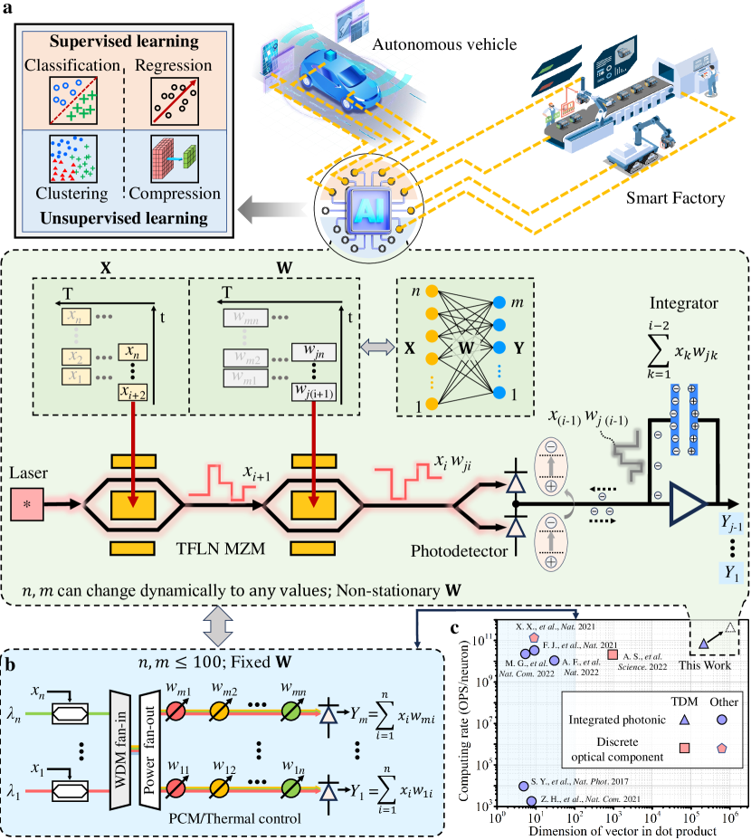
Artificial intelligence (AI) has been increasingly adopted in various fields including autonomous vehicles, smart buildings, and smart factories, as illustrated in Fig. 1a. Central to AI systems are tensor core processors, which are expected to exhibit several key characteristics:
-
•
High-speed, large-scale matrix-vector multiplication: These processors must efficiently process data from diverse devices for tasks like classification (supervised learning) and clustering (unsupervised learning), as depicted in Fig. 1a. Crucially, they perform matrix-vector multiplication and adjust input (fan-in) and output (fan-out) sizes in network layers on demand.
-
•
Rapid weight updates: For accurate and efficient training, it is crucial to employ “hardware-in-the-loop” training Pai_Science_2023 ; buckley2023photonic ; filipovich2021silicon ; huang2021silicon . This process incorporates real-time processor feedback into the weight update loop, accounting for processor imperfections and environmental changes. Rapid weight updates not only expedite training but also facilitate “on-the-fly” online learning, which is particularly advantageous for applications in autonomous vehicles pan2020imitation .
-
•
Low energy consumption and small form factor: AI systems typically deploy multiple processors (see Fig. 1a). Therefore, these processors need to be energy-efficient and compact.
However, finding a tensor core processor that meets all these requirements simultaneously is challenging lee2018unpu ; Mythic2022 ; fu2023photonic ; mourgias2022noise ; ashtiani2022chip ; zhang2021optical ; thakur2018large ; shastri2021photonics ; song2021recent . Traditional digital computers struggle with the speed and energy efficiency of matrix algebra due to Joule heating, electromagnetic crosstalk, and parasitic capacitance feldmann2021parallel ; miller2017attojoule . In contrast, photonic integrated circuits (PICs)-based tensor core processors provide high computational speed, low energy consumption, and compactness, overcoming the aforementioned issues spall2022hybrid ; feldmann2021parallel ; shen2017deep ; xu2021optical . However, an integrated photonic tensor core (IPTC) capable of large-scale matrix-vector multiplication with adjustable input (fan-in) and output (fan-out) sizes, alongside rapid weight updates, remains a significant challenge. For example, IPTCs utilizing wavelength-division multiplexing (WDM) are inherently limited by the number of available wavelength channels, which limits the fan-in size in a neural network layer (see Fig. 1b) shastri2021photonics ; tait2017neuromorphic . Additionally, IPTCs based on interferometric meshes shen2017deep ; fu2023photonic require a single laser source but face scalability issues due to the multitude of directional couplers and phase shifters involved. To date, all IPTC models are confined to either static (non-volatile) weights, like those utilizing phase change materials feldmann2021parallel ; zhou2023memory , or slowly updated (volatile) weights through thermal control shen2017deep , which are power intensive, rendering them unsuitable for “hardware-in-the-loop” training meng2023compact . While these platforms can achieve high computational speeds, they are limited to small-scale vector operations and inference tasks.
Here, we introduce an IPTC utilizing time-division multiplexing (TDM) sludds2022delocalized ; de2021codesigned with thin-film lithium niobate (TFLN) photonics and charge-integration photoreceivers (Fig. 1b). Our processor significantly surpasses current photonic platforms xu202111 ; feldmann2021parallel ; mourgias2022noise ; ashtiani2022chip ; sludds2022delocalized ; shen2017deep ; zhang2021optical , as quantified in Fig. 1c. This fully integrated processor, comprising only two TFLN modulators, a III-V laser, and a charge-integration photoreceiver, can implement an entire layer of a neural network (Fig. 1b). By modulating the integration time of the charge-integration photoreceiver, we can dynamically adjust the matrix-vector multiplication’s fan-in size. Our processor can perform matrix-vector multiplication with a fan-in size of 131,072—far exceeding the capacity of previously reported IPTCs by four orders of magnitude greater (Fig. 1c).
Leveraging the high modulation speed of TFLN modulators and the fast accumulation operation of charge-integration photoreceivers wang2018integrated ; xu2022dual ; lin2022high , our processor achieves a computational speed of 65 GOPS per neuron, including concurrent weight updates—a speed hitherto unachieved, enabling fast “hardware-in-the-loop” training. Our device successfully classifies (supervised learning) and clusters (unsupervised learning) 112112-pixel images via “hardware-in-the-loop” training. Notably, our device is the first to provide a solution for multiplications involving two negative numbers. Thus, our device is the first one capable of performing “hardware-in-the-loop” training for clustering images. For compactness, our processor employs hybrid integration techniques to combine our TFLN chip with III-V lasers and photodetectors billah2018hybrid .
Concept and principle
Figure 1a presents a schematic of the proposed TDM-based IPTC, consisting of two cascaded TFLN Mach-Zehnder modulators, one laser, and one charge-integration photoreceiver. Our device uses charge-integration photoreceivers for accumulative operations and leverages TFLN Mach-Zehnder modulators for high-speed multiplication operations and weight updates. Therefore, using just four physical components, our IPTC can implement an entire layer of a neural network with fan-in and fan-out. and can be dynamically adjusted as needed. In contrast, the conventional WDM-based IPTC requires modulators, weight additions, and large-bandwidth photodetectors to implement a layer with fan-in and fan-out (see Fig. 1b).
The input data is flattened into a vector and modulated on a time basis becoming , where is the dimension of the input vector, is the Dirac delta function, and is the baud rate of the modulator. Simultaneously, the weights of the row are flattened into a vector becoming , where is a delay time which needs to be calibrated to guarantee each weight vector element can be correctly multiplied by the corresponding element of the input vector. At a time, , is modulated by performing the multiplying operation of the element. In this way, the multiplication of all of the elements of and are multiplied sequentially and then summed by the integrator. Therefore, the dot product operation between the input and weight vectors, , can be obtained by simply reading the output voltage of the integrator through an analog-to-digital converter whose sampling rate only needs to be . By adjusting the integration time of the integrator, can be changed and made to be very large. By computing the output of each node sequentially in a time series, our device can implement an entire layer of a neural network. Therefore, our processor can offer the flexibility to dynamically change the sizes of fan-in and fan-out in a layer.
Prototype
Figure 2a presents a photo of a prototype of our device. Additionally, Figs. 2b-2e provide zoomed-in micrographs of the fabricated TFLN chip, flip-chip photodetectors, traveling-wave electrode of the modulator, and laser, respectively. More details regarding the fabrication of the TFLN chip can be found in Methods. Using flip-chip bonding technology, two photodetectors (marked as PD1 and PD2), in a balanced detection scheme, were affixed above two grating couplers, as shown in Fig. 2c. The laser and TFLN chip were connected using a photonic wire bond whose shape can be adapted to match the actual positions of the waveguide facets (see Fig. 2e). As shown in the right side of Fig. 2c, we also connected our TFLN chip with a fiber array by photonic wire bonds for calibrating bias voltages and delay time, and assisting in the multiplication involving two negative numbers. Details regarding the photonic wire bonding technology are shown in Methods and Supplementary note 1. Figure 2f illustrates the relative heights of the TFLN chip, laser, and photodetectors.
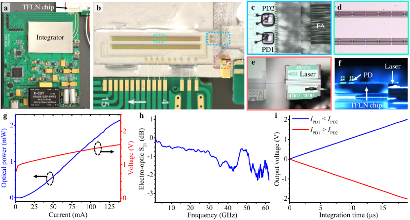
Figure 2g presents the light-current-voltage (L-I-V) curves for the light coupled into the TFLN chip from the laser with a wavelength of 1307.22 nm. More detailed performances of the hybrid integrated laser are shown in Supplementary note 2. Thanks to the periodic capacitively loaded traveling-wave electrodes (see Fig. 2d) chen2022high ; kharel2021breaking ; xu2022dual , the 3-dB electro-optic bandwidth of our modulator is broader than 60 GHz (see Fig. 2h). The output voltage of the integrator linearly increases with the integration time for a constant input optical power (see Fig. 2i). In a balanced detection scheme, when the optical power received by PD1 is lower than that received by PD2, the output voltage variation of the integrator is positive and, when it is higher than that received by PD2, the output voltage variation of the integrator is negative. This means that the proposed photoreceiver can perform add and subtract operations in the matrix-vector multiplication. More details regarding the charge integrator and the corresponding electrical controlling circuit can be found in Supplementary note 3.
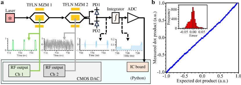
Dot product accelerator
In this section, we demonstrate how to perform a dot product operation between two vectors using our device. A schematic of data flows through our device is shown in Fig. 3a. Python, an open-source programming language, was used to control all our devices. Here, we implemented commercial complementary metal–oxide–semiconductor (CMOS) digital-to-analog converters (DACs) to drive our modulators ahmed2020dual . We recorded 3780 photonic dot product measurements using our device by randomly varying the two vectors. The dimension of each vector was set as 131072 which is limited by our CMOS DACs, and two vectors were separately modulated by the two modulators with a modulation rate of 32.5 Gbaud enabling a computational speed of 65 GOPS per neuron. The time delay between two vectors was initially calibrated to guarantee that each element of the first vector can be correctly multiplied by the corresponding element of the second vector. More details regarding the experimental setup can be found in Supplementary note 4. The measured output voltage (i.e., dot product result), scaled between and , as a function of the expected dot product result, is shown in Fig. 3b. Compared with the expected dot product result, the error of the measured one has a standard deviation of 0.02 (6.64 bits) more than the 5 bits of precision required for performing AI tasks gokmen2019marriage . Moreover, our device can achieve an energy consumption of approximately 800 fJ per operation in laser and modulators.
Images classification
Having shown that our device can perform large-scale dot product operation with a computational speed of 65 GOPS per neuron and a precision of 6.64 bits, in the next step, we built a multilayer perceptron (see Fig. 4a) and tested it against the MNIST large-scale handwritten digit database jansson2022scale ; pinkus1999approximation . Here, the multilayer perceptron includes 4 layers: an input layer, two hidden layers, and an output layer. Each handwritten digit image, having pixels, was flattened into a vector as the input of the first layer. The number of nodes in the first and second hidden layers was set to 70 and 300, respectively, and the leaky ReLU function was used for the nonlinear activation function khotanzad1990classification .
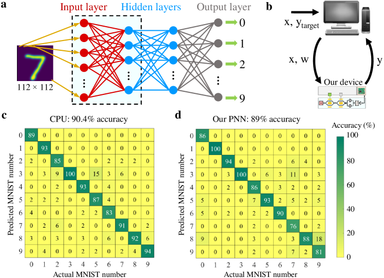
Classification is a supervised learning AI task that requires labeled data to train the model. Our multilayer perceptron model was trained with 3000 labeled digit images using a “hardware-in-the-loop” training (one type of online training) scheme (see Fig. 4b) that our IPTC performs forward propagation. At the same time, the electronic computer handles nonlinearity function and backpropagation. Weight vectors were updated by the stochastic gradient descent method amari1993backpropagation , allowing individual samples to be trained iteratively. The training process from forward propagation to backpropagation was repeated until convergence or until all samples were trained. More detail regarding the training algorithm can be found in Methods. To test the accuracy of the predictions, 500 test images were processed using our device. The confusion matrices illustrating the predictions for the different images with the calculated (completely run with CPU) and the experimental (run with our device) results are shown in Fig. 4c and 4c, respectively. Our device achieves an accuracy of 89 , showing good agreement with the calculated prediction accuracy of 90.4 .
Images clustering
Supervised learning successfully solved real-world challenges, but it has some drawbacks. One of the main limitations is that it requires a large number of accurately labeled data to train the model dalal2020analysing ; lin2023high . Creating such a database is a time-consuming and resource-intensive task that may not always be feasible. In contrast, unsupervised learning can be operated on unlabeled data to discover its underlying structure, offering an alternative approach for extracting data features.
We demonstrate the potential of our device for unsupervised learning AI tasks by utilizing it to cluster the MNIST large-scale handwritten digits with principle component analysis —one of the most commonly used unsupervised learning models lever2017points . Principle component analysis simplifies high-dimensional data by geometrically projecting them onto a limited number of principal components (PCs), i.e., unit vectors, to obtain the best summary of the data lever2017points . Clustering handwritten digits with principle component analysis involves two main steps: (1) finding the PCs for the unlabeled database, i.e., training the model, and (2) projecting the data onto each PC. Here, we used the power method to find the PCs that journee2010generalized
| (1) |
where , is a data matrix with column-wise zero empirical mean, and and are the total number of handwritten digits and the pixels of each digit, respectively. is a unit vector, obtained at the iteration, and is a randomly generated unit vector. converges to the first PC (PC1) when the variance of the projected points, , achieves the maximum value. The subsequent PCs can be obtained by a similar approach after subtracting all the previous PCs from . More details regarding the power method can be found in Methods.
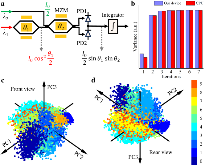
Through Eq. 1, we can know that the training involves the multiplication between two negative numbers. To achieve this, as illustrated in Fig. 5a, we found a solution that injecting light with a wavelength of into the second modulator, in addition to injecting light with a wavelength of into the first modulator. When the phase difference between the two arms of the first and second modulators is adjusted to and , respectively, the output of the balanced photodetectors becomes , indicating that this method enables the multiplication between two numbers with any signs. More details regarding the working principle can be found in Supplementary note 4. The convergence speed of our device is comparable with that of the CPU (see Fig. 5b), demonstrating that a dot product computing precision of 6.64 bits is enough to train the model using the power method.
Using the power method discussed above, we can obtain all the principal components. However, in general, the first few PCs are sufficient to summarize the data. In our example, the projections onto PC1-PC44 encompass 90 % of the features. To visualize the clustering result of the handwritten digits using our device, Figs. 5c and 5d present the projections onto PC1-PC3, accounting for 28.7 % of the features. Although only the first three PCs are used, the unlabeled handwritten digits can still be well clustered. Moreover, projecting the data onto the three PCs using our device is 5 times faster than a CPU (Intel i9-9900 @ 3.10GHz).
Discussion and conclusion
Our device’s computational speed, compactness, and capacity for large-scale dot product operations are summarized in Fig. 1c, where the performance of our device is compared to that of other state-of-the-art photonic devices xu202111 ; feldmann2021parallel ; mourgias2022noise ; ashtiani2022chip ; sludds2022delocalized ; shen2017deep ; zhang2021optical . Our device excels in all these aspects. Note that the performance of our device, demonstrated in this study, is currently limited by the drivers of the modulators used in our experiment. Based on the reported performance of the TFLN modulator mardoyan2022first ; wang2018integrated ; xu2022dual ; kharel2021breaking , our IPTC can achieve a computational speed of over 200 GOPS per neuron, and the vector dimension can extend to over one million (the dotted triangle shown in Fig. 1c) using more advanced DACs boasting higher speeds and larger memory capacity. Furthermore, because the TFLN modulator can simultaneously feature a low-drive voltage and a high modulation speed, in the future, the proposed IPTC can be directly driven by CMOS DACs without electronic amplifiers, providing a more cost-effective, compact, and energy-efficient solution ahmed2020dual .
To show the scalability of our solution, we proposed a photonic deep neural network which combines the advantages of TDM and WDM methods (see Fig. 6). In theory, the proposed network can process multiple tasks in parallel with a computational speed larger than 500 TOPS. As an example, the proposed neural network includes 4 layers: an input layer, two hidden layers, and an output layer. The matrix multiplication between the input layer and hidden layer 1 is performed by our expanded IPTC which consists of input TFLN modulators, weighted TFLN modulators, and charge-integration photoreceivers. input TFLN modulators allow the proposed network to process tasks in parallel. Input and weighted TFLN modulators are connected by power splitters and WDMs. The light from the weighted TFLN modulator is split into charge-integration photoreceivers by a WDM to convert the dot product results of each task into an analog voltage. Subsequently, electric delay lines with various delay times are connected to these charge-integration photoreceivers, respectively, ensuring that the output of each task is produced in a time sequence. Diode comparators are used to perform activation functions. In general, the node numbers in the hidden layers and the output layer are relatively small. Consequently, it is a good choice to utilize WDM-based IPTCs for conducting matrix multiplications between hidden layer 1 and hidden layer 2, as well as between hidden layer 2 and the output layer. Here, the bandwidth of the photodetectors used in the hidden layer 2 and the output layer only needs to achieve , where is the baud rate of the input TFLN modulator, resulting in a significant cost saving. According to the previous study zhang2021optical , the comb source can generate 90 wavelengths, indicating that , , and can take on a value of 90, where and are the number of nodes in the hidden layer 2 and output layer, respectively. Assuming a baud rate of 100 Gbaud per second for the input TFLN modulators, the proposed network can attain a computational speed exceeding 500 TOPS. Moreover, the proposed network is capable of completing 90 tasks within 0.125 microseconds even when . With the ability to process multiple tasks in parallel, the proposed neural network has significant potential in autonomous vehicles that need to simultaneously classify images from multiple cameras.
In summary, as far as we know, we have demonstrated the first TDM-based IPTC using the TFLN photonics and charge integration photoreceiver. Our device can perform large-scale matrix-vector multiplications with dynamically adjustable fan-in and fan-out sizes and facilitate rapid weight updates. Our device is the pioneering IPTC with the capability to handle matrix-vector multiplication that involves the multiplication between two negative numbers. It is capable of processing both supervised and unsupervised learning AI tasks. In this work, we demonstrated a single neuron as a proof-of-concept, but the proposed architecture can be scaled up to achieve parallel computing, as shown in Supplementary note 1. Thanks to its compatibility with current commercial optical transceivers, our solution has the potential to rapidly enter the commercial phase. By taking advantage of electronic and photonic analog computing, our research paves the way for developing a universal IPTC.
Method
Design and fabrication of TFLN chip
The proposed TFLN chip was fabricated using a wafer (NanoLN) consisting of a 360 nm thick, x-cut, y-propagating, LN thin film on a 500 m thick quartz handle with a 2 m SiO2 layer in between the two. The optical devices were patterned using optical lithography and etched using inductively coupled plasma. Then, a cladding layer with a 1 m thick SiO2 was deposited on the top of optical devices. Gold and heater electrodes were then patterned with a lift-off process. To achieve a low-voltage, high-bandwidth electro-optic solution, we used 1 cm-long, capacitively loaded, travelling-wave electrodes on our TFLN modulators. Our modulators exhibit a 3-dB electro-optic bandwidth broader than 67 GHz, a Vπ of 2.4 V, and an extinction ratio larger than 20 dB.
Photonic wire bonding process
Photonic wire bonding is a technique for building hybrid connections between disparate optical components, such as TFLN chips, lasers, and fiber arrays, using three-dimensional (3D) polymer waveguides created by in-situ, two-photon polymerization lindenmann2012photonic14 . In our case, the photonic wire bonds were used between the TFLN chip and the laser. We also used the photonic wire bonds in various locations of our hybrid photonic circuit for calibration and testing purposes. The hybridization process was carried out as follows: first, the TFLN chip, a fiber array (used in calibration and testing), and the laser were glued to an aluminum submount with a low alignment precision using ultraviolet curable epoxies; second, the photoresist was dispensed on the optical ports of the TFLN chip, fiber array, and laser; third, the photonic wire bonder (Vanguard Automation GmbH, SONATA1000) was used to expose the photoresist and develop the shape of the interconnecting photonic wires. More detailed performances of photonic wire bonds and the hybrid integrated laser are shown in Supplementary note 2.
Experimental setup
A vector network analyzer (Agilent N5227A) with a bandwidth of up to 67 GHz was used to characterize the electro-optic response of the fabricated modulator at a telecom wavelength of 1310 nm. To perform the dot product operation, our device was driven by CMOS DACs (Fujitsu, LEIA, 8 bits, 65 GSa per second). For comparison purposes, the machine learning algorithms are also executed using a CPU (Intel i9-9900 @ 3.10GHz). More detail can be found in Supplementary note 4.
The principle of the stochastic gradient descent method
For the multilayer perceptron, the weight vectors in this study were updated using the stochastic gradient descent method, allowing individual samples to be trained iteratively. The training was implemented using a labelled dataset , where is the network input, and is the target to be compared with the network output. In the forward propagation, the output vector, , of the layer can be given by
| (2) |
where represents the weight matrix between the and layers, is the activation function for the output of the layer, and .
Through backpropagation, the “error”, , of the layer can be calculated by
| (3) |
where means the transpose of , and in the case of our network only has 4 layers. Then, the weight matrix can be updated by
| (4) |
where , is the learning rate, and is the Hadamard product (element-wise multiplication operator).
In our “hardware-in-the-loop” training scheme, our IPTC performed forward propagation while the computer handled nonlinearity function and backpropagation. This training process from forward propagation to backpropagation was repeated until convergence or all samples were trained.
The principle of power method for finding all principle components
We can find each PC by repeating Eq. 1, but the matrix needs to be changed for different PCs. To find the k PC, , the matrix can be given by
| (5) |
where
| (6) |
, is a data matrix with column-wise zero empirical mean, and are the number of samples and the pixels of each digit image, respectively. means the sth PC.
Data availability
The data that supports the findings of this study are available from the corresponding authors upon reasonable request.
Code availability
The code used in this study is available from the corresponding authors upon reasonable request.
Acknowledgements This research was supported by the Natural Sciences and Engineering Research Council of Canada (NSERC), the SiEPICfab consortium, the B.C. Knowledge Development Fund (BCKDF), the Canada Foundation for Innovation (CFI), the Refined Manufacturing Acceleration Process (REMAP) network, the Canada First Research Excellence Fund (CFREF), and the Quantum Materials and Future Technologies Program. We thank NRC for providing lasers. We thank Simon Levasseur and Nathalie Bacon from the University Laval for their technical support. We thank Xin Xin for his help in the experiment setup. We thank Zhongguan Lin for his help in designing the electrical control circuits.
Author contributions Z.L., X.C., L.C. jointly conceived the idea. Z.L. designed the device with help from Y.L., M.X, and T.W., M.R., G.P., J.S., P.B., W.J. designed and fabricated DFB buried heterostructure lasers with spot size convertors. Y.Z. and K.W. fabricated the photonic chip. Z.L., S.X.Y., M.M., and J.S. performed the photonic wire bonding experiment. Z.L. assembled the entire device. Z.L. performed the experiments with help from J.S., A.S., M.H., Z.Z., O.E., X.G., W.S., and L.R.. W.C., H.M., S.S., B.S., X.Q., N.J., and S.Y.Y assisted with the theory and algorithm. Z.L., X.C., B.S., and L.C. supervised and coordinated the work. Z.L. and X.C. with help from B.S. wrote the manuscript with contributions from all co-authors.
Competing interests The authors declare no competing interests.
References
- \bibcommenthead
- (1) Pai, S., Sun, Z., Hughes, T.W., Park, T., Bartlett, B., Williamson, I.A.D., Minkov, M., Milanizadeh, M., Abebe, N., Morichetti, F., Melloni, A., Fan, S., Solgaard, O., Miller, D.A.B.: Experimentally realized in situ backpropagation for deep learning in photonic neural networks. Science 380(6643), 398–404 (2023)
- (2) Buckley, S.M., Tait, A.N., McCaughan, A.N., Shastri, B.J.: Photonic online learning: a perspective. Nanophotonics (2023)
- (3) Filipovich, M.J., Guo, Z., Al-Qadasi, M., Marquez, B.A., Morison, H.D., Sorger, V.J., Prucnal, P.R., Shekhar, S., Shastri, B.J.: Silicon photonic architecture for training deep neural networks with direct feedback alignment. Optica 9(12), 1323–1332 (2022)
- (4) Huang, C., Fujisawa, S., de Lima, T.F., Tait, A.N., Blow, E.C., Tian, Y., Bilodeau, S., Jha, A., Yaman, F., Peng, H.-T., et al.: A silicon photonic–electronic neural network for fibre nonlinearity compensation. Nature Electronics 4(11), 837–844 (2021)
- (5) Pan, Y., Cheng, C.-A., Saigol, K., Lee, K., Yan, X., Theodorou, E.A., Boots, B.: Imitation learning for agile autonomous driving. The International Journal of Robotics Research 39(2-3), 286–302 (2020)
- (6) Lee, J., Kim, C., Kang, S., Shin, D., Kim, S., Yoo, H.-J.: UNPU: An energy-efficient deep neural network accelerator with fully variable weight bit precision. IEEE Journal of Solid-State Circuits 54(1), 173–185 (2018)
- (7) Mythic: M1076 Analog Matrix Processor. https://mythic.ai/products/m1076-analog-matrix-processor/ Accessed 2022-09-30
- (8) Fu, T., Zang, Y., Huang, Y., Du, Z., Huang, H., Hu, C., Chen, M., Yang, S., Chen, H.: Photonic machine learning with on-chip diffractive optics. Nature Communications 14(1), 70 (2023)
- (9) Mourgias-Alexandris, G., Moralis-Pegios, M., Tsakyridis, A., Simos, S., Dabos, G., Totovic, A., Passalis, N., Kirtas, M., Rutirawut, T., Gardes, F., et al.: Noise-resilient and high-speed deep learning with coherent silicon photonics. Nature Communications 13(1), 5572 (2022)
- (10) Ashtiani, F., Geers, A.J., Aflatouni, F.: An on-chip photonic deep neural network for image classification. Nature 606(7914), 501–506 (2022)
- (11) Zhang, H., Gu, M., Jiang, X., Thompson, J., Cai, H., Paesani, S., Santagati, R., Laing, A., Zhang, Y., Yung, M., et al.: An optical neural chip for implementing complex-valued neural network. Nature communications 12(1), 457 (2021)
- (12) Thakur, C.S., Molin, J.L., Cauwenberghs, G., Indiveri, G., Kumar, K., Qiao, N., Schemmel, J., Wang, R., Chicca, E., Olson Hasler, J., et al.: Large-scale neuromorphic spiking array processors: A quest to mimic the brain. Frontiers in neuroscience 12, 891 (2018)
- (13) Shastri, B.J., Tait, A.N., Ferreira de Lima, T., Pernice, W.H., Bhaskaran, H., Wright, C.D., Prucnal, P.R.: Photonics for artificial intelligence and neuromorphic computing. Nature Photonics 15(2), 102–114 (2021)
- (14) Song, S., Kim, J., Kwon, S.M., Jo, J.-W., Park, S.K., Kim, Y.-H.: Recent progress of optoelectronic and all-optical neuromorphic devices: A comprehensive review of device structures, materials, and applications. Advanced Intelligent Systems 3(4), 2000119 (2021)
- (15) Feldmann, J., Youngblood, N., Karpov, M., Gehring, H., Li, X., Stappers, M., Le Gallo, M., Fu, X., Lukashchuk, A., Raja, A.S., et al.: Parallel convolutional processing using an integrated photonic tensor core. Nature 589(7840), 52–58 (2021)
- (16) Miller, D.A.: Attojoule optoelectronics for low-energy information processing and communications. Journal of Lightwave Technology 35(3), 346–396 (2017)
- (17) Spall, J., Guo, X., Lvovsky, A.I.: Hybrid training of optical neural networks. Optica 9(7), 803–811 (2022)
- (18) Shen, Y., Harris, N.C., Skirlo, S., Prabhu, M., Baehr-Jones, T., Hochberg, M., Sun, X., Zhao, S., Larochelle, H., Englund, D., et al.: Deep learning with coherent nanophotonic circuits. Nature photonics 11(7), 441–446 (2017)
- (19) Xu, S., Wang, J., Shu, H., Zhang, Z., Yi, S., Bai, B., Wang, X., Liu, J., Zou, W.: Optical coherent dot-product chip for sophisticated deep learning regression. Light: Science & Applications 10(1), 221 (2021)
- (20) Tait, A.N., De Lima, T.F., Zhou, E., Wu, A.X., Nahmias, M.A., Shastri, B.J., Prucnal, P.R.: Neuromorphic photonic networks using silicon photonic weight banks. Scientific reports 7(1), 1–10 (2017)
- (21) Zhou, W., Dong, B., Farmakidis, N., Li, X., Youngblood, N., Huang, K., He, Y., David Wright, C., Pernice, W.H., Bhaskaran, H.: In-memory photonic dot-product engine with electrically programmable weight banks. Nature Communications 14(1), 2887 (2023)
- (22) Meng, X., Zhang, G., Shi, N., Li, G., Azaña, J., Capmany, J., Yao, J., Shen, Y., Li, W., Zhu, N., et al.: Compact optical convolution processing unit based on multimode interference. Nature Communications 14(1), 3000 (2023)
- (23) Sludds, A., Bandyopadhyay, S., Chen, Z., Zhong, Z., Cochrane, J., Bernstein, L., Bunandar, D., Dixon, P.B., Hamilton, S.A., Streshinsky, M., et al.: Delocalized photonic deep learning on the internet’s edge. Science 378(6617), 270–276 (2022)
- (24) De Marinis, L., Catania, A., Castoldi, P., Bruschi, P., Piotto, M., Andriolli, N.: A codesigned photonic electronic mac neuron with adc-embedded nonlinearity. In: CLEO: Science and Innovations, pp. 3–4 (2021). Optica Publishing Group
- (25) Xu, X., Tan, M., Corcoran, B., Wu, J., Boes, A., Nguyen, T.G., Chu, S.T., Little, B.E., Hicks, D.G., Morandotti, R., et al.: 11 TOPS photonic convolutional accelerator for optical neural networks. Nature 589(7840), 44–51 (2021)
- (26) Wang, C., Zhang, M., Chen, X., Bertrand, M., Shams-Ansari, A., Chandrasekhar, S., Winzer, P., Lončar, M.: Integrated lithium niobate electro-optic modulators operating at CMOS-compatible voltages. Nature 562(7725), 101–104 (2018)
- (27) Xu, M., Zhu, Y., Pittalà, F., Tang, J., He, M., Ng, W.C., Wang, J., Ruan, Z., Tang, X., Kuschnerov, M., et al.: Dual-polarization thin-film lithium niobate in-phase quadrature modulators for terabit-per-second transmission. Optica 9(1), 61–62 (2022)
- (28) Lin, Z., Lin, Y., Li, H., Xu, M., He, M., Ke, W., Tan, H., Han, Y., Li, Z., Wang, D., et al.: High-performance polarization management devices based on thin-film lithium niobate. Light: Science & Applications 11(1), 93 (2022)
- (29) Billah, M.R., Blaicher, M., Hoose, T., Dietrich, P.-I., Marin-Palomo, P., Lindenmann, N., Nesic, A., Hofmann, A., Troppenz, U., Moehrle, M., et al.: Hybrid integration of silicon photonics circuits and InP lasers by photonic wire bonding. Optica 5(7), 876–883 (2018)
- (30) Mwase, C., Jin, Y., Westerlund, T., Tenhunen, H., Zou, Z.: Communication-efficient distributed AI strategies for the IoT edge. Future Generation Computer Systems (2022)
- (31) Beath, C., Becerra-Fernandez, I., Ross, J., Short, J.: Finding value in the information explosion. MIT Sloan Management Review (2012)
- (32) Lin, Z., Yu, S., Chen, Y., Cai, W., Lin, B., Song, J., Mitchell, M., Hammood, M., Jhoja, J., Jaeger, N.A., et al.: High-performance, intelligent, on-chip speckle spectrometer using 2D silicon photonic disordered microring lattice. Optica 10(4), 497–504 (2023)
- (33) Rabah, K.: Convergence of AI, IoT, big data and blockchain: a review. The lake institute Journal 1(1), 1–18 (2018)
- (34) Chen, G., Chen, K., Gan, R., Ruan, Z., Wang, Z., Huang, P., Lu, C., Lau, A.P.T., Dai, D., Guo, C., et al.: High performance thin-film lithium niobate modulator on a silicon substrate using periodic capacitively loaded traveling-wave electrode. APL Photonics 7(2), 026103 (2022)
- (35) Kharel, P., Reimer, C., Luke, K., He, L., Zhang, M.: Breaking voltage–bandwidth limits in integrated lithium niobate modulators using micro-structured electrodes. Optica 8(3), 357–363 (2021)
- (36) Ahmed, A.H., El Moznine, A., Lim, D., Ma, Y., Rylyakov, A., Shekhar, S.: A dual-polarization silicon-photonic coherent transmitter supporting 552 Gb/s/wavelength. IEEE Journal of Solid-State Circuits 55(9), 2597–2608 (2020)
- (37) Gokmen, T., Rasch, M.J., Haensch, W.: The marriage of training and inference for scaled deep learning analog hardware. In: 2019 IEEE International Electron Devices Meeting (IEDM), pp. 22–3 (2019). IEEE
- (38) Jansson, Y., Lindeberg, T.: Scale-invariant scale-channel networks: Deep networks that generalise to previously unseen scales. Journal of Mathematical Imaging and Vision 64(5), 506–536 (2022)
- (39) Pinkus, A.: Approximation theory of the MLP model in neural networks. Acta numerica 8, 143–195 (1999)
- (40) Khotanzad, A., Lu, J.-H.: Classification of invariant image representations using a neural network. IEEE Transactions on Acoustics, Speech, and Signal Processing 38(6), 1028–1038 (1990)
- (41) Amari, S.-i.: Backpropagation and stochastic gradient descent method. Neurocomputing 5(4-5), 185–196 (1993)
- (42) Dalal, K.R.: Analysing the role of supervised and unsupervised machine learning in iot. In: 2020 International Conference on Electronics and Sustainable Communication Systems (ICESC), pp. 75–79 (2020). IEEE
- (43) Lever, J., Krzywinski, M., Altman, N.: Points of significance: Principal component analysis. Nature methods 14(7), 641–643 (2017)
- (44) Journée, M., Nesterov, Y., Richtárik, P., Sepulchre, R.: Generalized power method for sparse principal component analysis. Journal of Machine Learning Research 11(2) (2010)
- (45) Mardoyan, H., Almonacil, S., Jorge, F., Pittalà, F., Xu, M., Krueger, B., Blache, F., Duval, B., Chen, L., Yan, Y., et al.: First 260-GBd single-carrier coherent transmission over 100 km distance based on novel arbitrary waveform generator and thin-film lithium niobate I/Q modulator. In: European Conference and Exhibition on Optical Communication, pp. 3–2 (2022). Optica Publishing Group
- (46) Lindenmann, N., Balthasar, G., Hillerkuss, D., Schmogrow, R., Jordan, M., Leuthold, J., Freude, W., Koos, C.: Photonic wire bonding: a novel concept for chip-scale interconnects. Optics express 20(16), 17667–17677 (2012)