Selective-Area-Grown PbTe-Pb Planar Josephson Junctions for Quantum Devices
Abstract
Planar Josephson junctions are predicted to host Majorana zero modes. The material platforms in previous studies are two dimensional electron gases (InAs, InSb, InAsSb and HgTe) coupled to a superconductor such as Al or Nb. Here, we introduce a new material platform for planar JJs, the PbTe-Pb hybrid. The semiconductor, PbTe, was grown as a thin film via selective area epitaxy. The Josephson junction was defined by a shadow wall during the deposition of the superconductor Pb. Scanning transmission electron microscopy reveals a sharp semiconductor-superconductor interface. Gate-tunable supercurrent and multiple Andreev reflections are observed. A perpendicular magnetic field causes interference patterns of the switching current, exhibiting Fraunhofer-like and SQUID-like behaviors. We further demonstrate a prototype device for Majorana detection, wherein phase bias and tunneling spectroscopy are applicable.
Semiconductor-superconductor hybrids with strong spin-orbit interaction can exhibit intriguing phases of matter, notably topological superconductivity [1, 2]. One promising platform involves coupling a two-dimensional electron gas (2DEG) with a superconductor to create a planar Josephson junction (JJ). Majorana zero modes are predicted to localize near the two edges of the JJ [3, 4]. In comparison to nanowire platforms [5, 6, 7], the key advantage of this platform is the phase bias across the junction. This additional experimental knob can reduce the critical magnetic field required for Majoranas. Previous studies have employed HgTe, InAs, InSb and InAsSb as the 2DEG materials [8, 9, 10, 11]. Appealing experimental progress, including supercurrent interference [12, 13, 14, 15, 16], -junction physics [17, 18, 19] and zero-bias conductance peaks [20, 21, 22, 23] have been demonstrated in corresponding devices. Theoretical studies have systematically explored the physics of planar JJs and the roadmap toward braiding and topological quantum computation [24, 25, 26, 27]. The absence of end-to-end correlations of zero-bias peaks implies that the current experiments are limited by disorder [23]. Eliminating disorder is of critical importance for Majorana experiments and topological quantum computation [28, 29].
Here, we present the PbTe-Pb hybrid as a new planar JJ material platform for exploring topological superconductivity and other potential applications, such as gate tunable qubits [30, 31, 32]. While the PbTe-Pb hybrid has recently been proposed in its nanowire form as a Majorana candidate [33] with promising experimental progress [34, 35, 36, 37, 38, 39, 40, 41], in this paper, we realize its 2DEG version, motivated by the Majorana proposals for topological planar JJs [3, 4]. Selective area growth (SAG) of PbTe film has been previously achieved on InP, a substrate that is lattice-mismatched with PbTe [42]. In this work, the SAG PbTe film is grown on a lattice-matched substrate to minimize disorder. The junction was defined using a shadow wall during the in-situ growth of the superconductor. This process prevents direct etching of the superconductor on the junction. Subsequent fabrication steps also kept the junction region intact, further mitigating potential sources of disorder. Transport characterization of the planar JJs reveals a gate-tunable supercurrent and its interference in a perpendicular magnetic field. In the end, we demonstrate the design of a prototype device for Majorana detection.
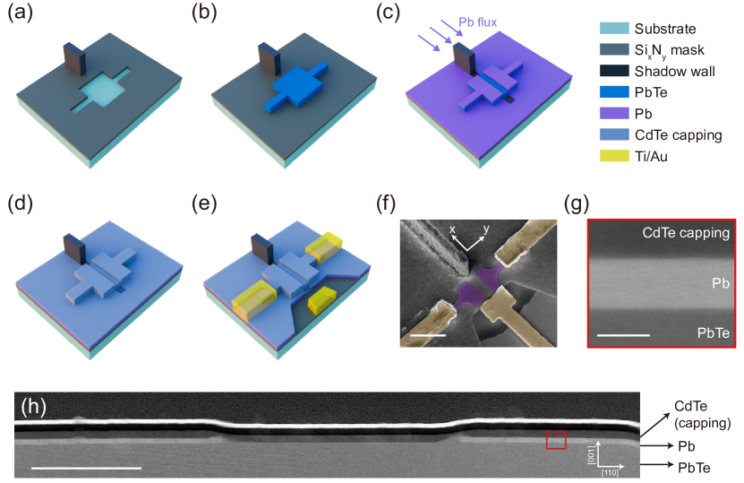
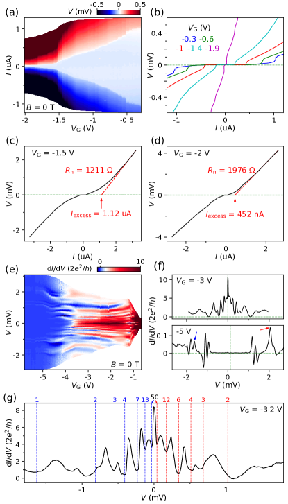
Figure 1 briefly illustrates the device design, growth procedure, and material analysis. We started with a CdTe/Pb1-xEuxTe substrate [39, 40, 41] and covered it with a thin SiN dielectric layer. The value of was estimated to be 0.08. A Hydrogen SilsesQuioxane (HSQ) shadow wall was fabricated prior to the Pb1-xEuxTe growth [34]. A square-shaped pattern with two additional bars (wire shape) was then defined by etching the SiN film in a process of electron beam lithography, as shown in Fig. 1(a). The square pattern defines the semiconductor 2DEG while the two extra bars are for source/drain contacts. The PbTe (blue) thin film was then selectively grown within the etched region, as depicted in Fig. 1(b). To ensure selectivity during the PbTe growth, the substrate was heated to 327 ∘C. The estimated thickness of the PbTe film was 80 nm. For the superconductor growth, the chip was then cooled using a liquid nitrogen stage, and the Pb film was deposited at a tilted angle. This configuration allowed the HSQ wall to shadow a portion of the film, defining the Josephson junction region, as illustrated in Fig. 1(c). The entire chip was then capped with a thin CdTe layer to prevent oxidation of the Pb film, as shown in Fig. 1(d).
The device fabrication was similar to that in Ref. [38]. To prevent short-circuits, most of the Pb film on the substrate was etched using ion milling. Note that the Pb film on the PbTe device and the core region of the JJ, defined by the shadow growth, were kept intact. Electrode contacts and a side gate were then deposited (Fig. 1(e)) through evaporation of Ti/Au. Prior to the metal deposition, Ar plasma etching was performed to remove the capping layer for ohmic contacts. Figure 1(f) shows the scanning electron micrograph (SEM) of a representative device. The Pb film (capped by CdTe) on PbTe is false-colored (violet) for clarity. The side gate was positioned in a U-shaped region where the Pb film has been etched away using ion milling.
To characterize the semiconductor-superconductor interface, we performed the scanning transmission electron microscopy (STEM) on a measured device (referred to as device A, see Figs. 2-3 for its transport characterization). Figure 1(g) shows the PbTe-Pb-CdTe layered structure. The PbTe-Pb and Pb-CdTe (capping) interfaces appear clean and sharply defined. These sharp interfaces are crucial for high-quality and low-disordered quantum devices. We further show an overview of the cross-section of the JJ in Fig. 1(h), corresponding to a cut through the midpoint of the junction, along the -axis (parallel to the current flow, as depicted in Fig. 1(f)). Fig. 1(g) is an enlarged view of the red box in Fig. 1(h). The Pb film appears flat and uniform on the device scale. The middle region in Fig. 1(h) is the shadowed region (the junction), corresponding to the PbTe part not covered by Pb. The shadowed region is flat and uniformly capped by a CdTe layer, suggesting a low level of disorder. The dark and white layers above the CdTe capping are evaporated Ti/Au, not part of the device but were introduced after the measurement for the processes of focused ion beam and STEM to enhance surface conductivity. Further details regarding the material analysis (e.g. atomic resolution STEM) are provided in Fig. S1 in the Supporting Information.
Next we show the basic transport properties of device A in Fig. 2, with its corresponding SEM provided in Fig. S1. All measurements were performed in a dilution fridge at a base temperature below 50 mK. Figure 2(a) illustrates the current-voltage (-) characteristic and its gate () dependence at zero magnetic field ( = 0 T). represents the current passing through the JJ, and denotes the voltage drop across the JJ. The light blue region corresponds to the supercurrent regime characterized by zero resistance, see Fig. 2(b) for line cuts. The sweeping direction of ranged from negative to positive. The measurement circuit was standard two-terminal. Thus a series resistance, contributed by the fridge filters and the device contacts, was subtracted, see Fig. S2 in the Supporting Information for a detailed analysis. The switching current can be gate-tuned from 0 to 1 A with varying from -2 V to -0.3 V. The retrapping current , defined by the switching point in the negative bias branch, is close to , suggesting an over-damped nature for device A.
To extract the excess current (), a higher current bias was applied, as shown in Fig. 2(c). From the linear fit at , we can extract the normal state resistance 1.2 k. While the exact size of the superconducting gap () is unknown, we assumed it to be 1 meV based on measurements on nanowire devices [40]. The intercept of the linear fit on the -axis gives the estimated , which is approximately 1.12 A. Consequently, the value of can be estimated to be 1.344, corresponding to a junction transparency of 0.81 [43, 44]. Note that the transparency is gate-dependent, see Fig. 2(d) for another example with a transparency of 0.7.
Figure 2(e) presents the differential conductance as a function of and at zero magnetic field. In the open regime (upper panel of Fig. 2(f)), a zero-bias peak is observed and attributed to supercurrent. The subgap peaks/dips are likely a results of multiple Andreev reflections (MARs) [44, 45]. The lower panel of Fig. 2(f) corresponds to the tunneling regime. The subgap conductance is suppressed and negative differential conductance is observed near the gap edges, reminiscent of gap spectroscopy of S-NW-S devices (S for superconductor and NW for nanowire) [38]. However, the complexity arises here as the JJ cannot be simplified as a tunnel barrier due to its large size. The side gate also does not uniformly deplete the JJ: the junction region close to the gate gets depleted first. Additionally, the JJ shadowing is not uniform due to parasitic growth on the shadow wall (see Fig. S1 for its SEM). This non-uniformity can lead to a spatially non-uniform induced gap. The line shape in the lower panel of Fig. 2(f) is not centered near zero bias, but around = 0.12 mV (the green dashed line), possibly due to the aforementioned mechanisms. Figure 2(g) shows a line cut with dashed lines indicating the positions of MARs. Note that conductance dips (resistance peaks) should mark the positions of MARs for a JJ in the high transparency regime [45]. Due to the non-zero offset of the midpoint, we assumed the value of to be 1.63 meV for the negative bias branch and 2.05 meV for the positive bias branch, corresponding to the positions of the two peaks in Fig. 2(f) (the blue and red arrows), respectively. The expected MAR positions, ( is an integer, see labeling), roughly align with the conductance dips with minor deviations.
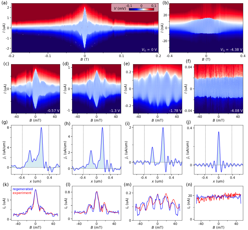
We then fix the gate voltage and scan a magnetic field () that is perpendicular to the device substrate. Figure 3(a) shows such an example for device A at = 0 V. The zero-field switching current is 2 A. This value is significantly suppressed for at 0.2 T. The suppression is not monotonic, but accompanied by oscillations of . These oscillations arise from the interference of the supercurrent distributed within the junction. The perpendicular induces a spatial variation of the phase gradient across the JJ along the -axis (see Fig. 1(f) for its labeling), in the form of . is the flux quantum (), and is the effective junction length (along the -axis). The switching current of the JJ is a phase-sensitive summation (integration) of the supercurrent distributed over the -axis: , leading to oscillations of in . is the critical supercurrent density, which is a function . This model assumes a sinusoidal current-phase relation. For more negative (Fig. 3(b)), the JJ exhibits a switching current of 20 nA, which is two orders of magnitude smaller than that of Fig. 3(a). The supercurrent is monotonically suppressed without the oscillations. This observation suggests that near the pinched-off regime, the supercurrent is “squeezed” into a narrow channel within the JJ, where spatial variation of the phase gradient is effectively suppressed.
To elucidate the gradual evolution, we present four successive scans in Figs. 3(c-f), setting between Figs. 3(a) and 3(b) (additional scans can be found in Fig. S3 in the Supporting Information). In Fig. 3(c), the central lobe is much “taller” (in ) than the side lobes, indicating a Fraunhofer-like interference pattern where the supercurrent is distributed throughout the junction. Note that if along the -axis is uniform, the width of the central lobe should be twice that of the side lobes. However, in Fig. 3(c), the central lobe width ( 18 mT) is only slightly larger than that of the side lobes ( 14.8 mT). This narrowing of the central lobe suggests that is not uniform along the -axis, possibly due to imperfections of the fabrication process or a spatially varying junction length (). Figure 3(g) shows the calculated for Fig. 3(c), employing a method based on Fourier transform [12]. The distribution is indeed inhomogeneous and reveals two dominating peaks. The JJ edges are denoted as the two vertical dashed lines. The width of the JJ is 780 nm, and we define = 0 as the JJ midpoint. We have also implemented a slightly different method from Dynes and Fulton [46], yielding a qualitatively similar distribution (see Fig. S4 in the Supporting Information).
As becomes more negative, the height of the central lobe decreases, and the oscillations become more SQUID-like, as shown in Fig. 3(e). The corresponding in Fig. 3(i) shows two peaks with other regions being depleted, confirming its “double-slit” nature. The origin of this current distribution, similar to two edge modes, is currently unknown. Based on and the oscillation period = 14.8 mT, we can estimate the effective junction area 0.14 m2. In Fig. 3(f), is quite small ( 20 nA) at more negative and the interference pattern is gone. Correspondingly, the supercurrent distribution (Fig. 3(j)) transforms into a single narrow peak.
In Figs. 3(k-n), we reconstruct the oscillation patterns of using the calculated in Figs. 3(g-j) as an input. Plugging this into the formula, we reconstruct (the blue curves), and compare it to the (the red curves) extracted from Figs. 3(c-f). The qualitative agreement suggests that the calculated is reliable. Note that we did not consider the London penetration depth and the effect of flux focusing, i.e. is purely the spacing between the two Pb films. Including those effects would cause a smaller spacing of the two peaks in in Figs. 3(g-i). For supercurrent interference in more devices, see Fig. S5 in the Supporting Information.
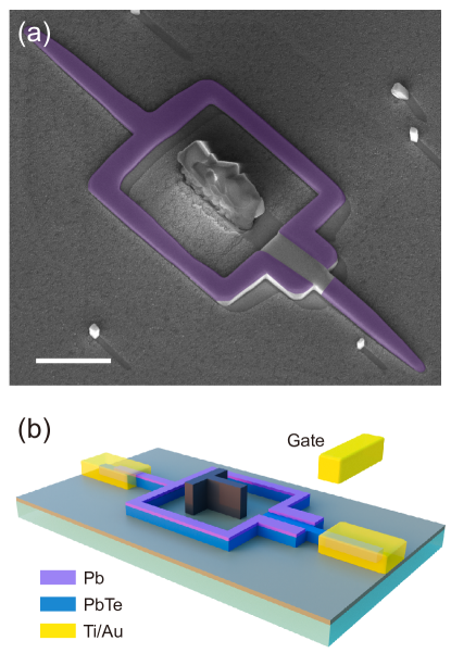
After establishing the feasibility of the PbTe-Pb hybrid as a planar JJ platform, Figure 4 presents a prototype device designed for future Majorana detection. To enable the application of phase bias, the two bars of the planar JJ are interconnected, forming a PbTe nanowire network loop, as depicted in Fig. 4(a). The shadow wall, fabricated within the loop, defines the JJ region on the PbTe film. The violet region represents the Pb film (capped by CdTe) on PbTe. The nanowire loop and the planar JJ together form an ac SQUID. The phase drop across the planar JJ can be tuned by the flux penetrating through the loop, further controlled by a small out-of-plane magnetic field. Figure 4(b) shows the schematic of the device. The source contact is deposited on the PbTe nanowire, connecting to one edge of the planar JJ for probing its edge state. The drain contact connects to the ac SQUID. Top gates can be fabricated after the deposition of a dielectric layer (not drawn for clarity). One top gate can be used to tune the tunnel barrier height in the PbTe nanowire region between the source contact and the edge of the JJ. Another gate (not drawn for clarity) can be deposited on top of the junction region to tune its electrochemical potential. This device setup, achieved mainly through selective area growth, is equivalent to Ref. [20, 21], where tunneling spectroscopy can be performed to detect a single Majorana zero mode. For the detection of two Majoranas and their correlation, three-terminal devices should also be possible through a more sophisticated geometry of the shadow wall and the network loops.
In summary, we have demonstrated the selective area growth of PbTe-Pb hybrid planar Josephson junctions as a potential Majorana material platform. Unlike the previous 2DEG top-down approach, the junction region was formed during the growth process instead of by wet etching. This approach allows us to keep the core region of the JJ intact and may reduce disorder. Basic transport calibration reveals a gate-tunable supercurrent and supercurrent interference in a perpendicular magnetic field, characteristic for a planar JJ. We also present the growth of a prototype device where the phase bias can be applied and tunneling spectroscopy can be performed to detect Majorana zero modes.
Acknowledgement We thank Hechen Ren for valuable comments. This work is supported by Tsinghua University Initiative Scientific Research Program, National Natural Science Foundation of China (92065206) and the Innovation Program for Quantum Science and Technology (2021ZD0302400). Raw data and processing codes within this paper are available at https://doi.org/10.5281/zenodo.10213760
References
- Read and Green [2000] N. Read and D. Green, Paired states of fermions in two dimensions with breaking of parity and time-reversal symmetries and the fractional quantum hall effect, Phys. Rev. B 61, 10267 (2000).
- Kitaev [2001] A. Y. Kitaev, Unpaired Majorana fermions in quantum wires, Physics-Uspekhi 44, 131 (2001).
- Hell et al. [2017] M. Hell, M. Leijnse, and K. Flensberg, Two-dimensional platform for networks of Majorana bound states, Phys. Rev. Lett. 118, 107701 (2017).
- Pientka et al. [2017] F. Pientka, A. Keselman, E. Berg, A. Yacoby, A. Stern, and B. I. Halperin, Topological superconductivity in a planar Josephson junction, Phys. Rev. X 7, 021032 (2017).
- Lutchyn et al. [2010] R. M. Lutchyn, J. D. Sau, and S. Das Sarma, Majorana fermions and a topological phase transition in semiconductor-superconductor heterostructures, Phys. Rev. Lett. 105, 077001 (2010).
- Oreg et al. [2010] Y. Oreg, G. Refael, and F. von Oppen, Helical liquids and Majorana bound states in quantum wires, Phys. Rev. Lett. 105, 177002 (2010).
- Wang et al. [2022] Z. Wang, H. Song, D. Pan, Z. Zhang, W. Miao, R. Li, Z. Cao, G. Zhang, L. Liu, L. Wen, R. Zhuo, D. E. Liu, K. He, R. Shang, J. Zhao, and H. Zhang, Plateau regions for zero-bias peaks within 5 of the quantized conductance value , Phys. Rev. Lett. 129, 167702 (2022).
- König et al. [2007] M. König, S. Wiedmann, C. Brüne, A. Roth, H. Buhmann, L. W. Molenkamp, X.-L. Qi, and S.-C. Zhang, Quantum spin Hall insulator state in HgTe quantum wells, Science 318, 766 (2007).
- Shabani et al. [2016] J. Shabani, M. Kjaergaard, H. J. Suominen, Y. Kim, F. Nichele, K. Pakrouski, T. Stankevic, R. M. Lutchyn, P. Krogstrup, R. Feidenhans’l, S. Kraemer, C. Nayak, M. Troyer, C. M. Marcus, and C. J. Palmstrøm, Two-dimensional epitaxial superconductor-semiconductor heterostructures: A platform for topological superconducting networks, Phys. Rev. B 93, 155402 (2016).
- Yi et al. [2015] W. Yi, A. Kiselev, J. Thorp, R. Noah, B.-M. Nguyen, S. Bui, R. Rajavel, T. Hussain, M. Gyure, P. Kratz, Q. Qian, M. Manfra, V. Pribiag, L. Kouwenhoven, C. Marcus, and M. Sokolich, Gate-tunable high mobility remote-doped InSb/In1-xAlxSb quantum well heterostructures, Applied Physics Letters 106, 142103 (2015).
- Moehle et al. [2021] C. Moehle, C. Ke, Q. Wang, C. Thomas, D. Xiao, S. Karwal, M. Lodari, V. Kerkhof, R. Termaat, G. Gardner, G. Scappucci, M. Manfra, and S. Goswami, InSbAs two-dimensional electron gases as a platform for topological superconductivity, Nano Letters 21, 9990 (2021).
- Hart et al. [2014] S. Hart, H. Ren, T. Wagner, P. Leubner, M. Mühlbauer, C. Brüne, H. Buhmann, L. Molenkamp, and A. Yacoby, Induced superconductivity in the quantum spin Hall edge, Nature Physics 10, 638 (2014).
- Pribiag et al. [2015] V. Pribiag, A. Beukman, F. Qu, C. Cassidy, C. Charpentier, W. Wegscheider, and L. Kouwenhoven, Edge-mode superconductivity in a two dimensional topological insulator, Nature Nanotechnology 10, 593 (2015).
- Suominen et al. [2017] H. J. Suominen, J. Danon, M. Kjaergaard, K. Flensberg, J. Shabani, C. J. Palmstrøm, F. Nichele, and C. M. Marcus, Anomalous Fraunhofer interference in epitaxial superconductor-semiconductor Josephson junctions, Phys. Rev. B 95, 035307 (2017).
- Mayer et al. [2020] W. Mayer, M. Dartiailh, J. Yuan, K. Wickramasinghe, E. Rossi, and J. Shabani, Gate controlled anomalous phase shift in Al/InAs Josephson junctions, Nature Communications 11, 212 (2020).
- Elfeky et al. [2021] B. H. Elfeky, N. Lotfizadeh, W. F. Schiela, W. M. Strickland, M. Dartiailh, K. Sardashti, M. Hatefipour, P. Yu, N. Pankratova, H. Lee, V. E. Manucharyan, and J. Shabani, Local control of supercurrent density in epitaxial planar Josephson junctions, Nano Letters 21, 8274 (2021).
- Hart et al. [2017] S. Hart, H. Ren, M. Kosowsky, G. Ben-Shach, P. Leubner, C. Brüne, H. Buhmann, L. Molenkamp, B. Halperin, and A. Yacoby, Controlled finite momentum pairing and spatially varying order parameter in proximitized HgTe quantum wells, Nature Physics 13, 87 (2017).
- Ke et al. [2019] C. T. Ke, C. Moehle, F. de Vries, C. Thomas, S. Metti, C. Guinn, R. Kallaher, M. Lodari, G. Scappucci, T. Wang, R. Diaz, G. Gardner, M. Manfra, and S. Goswami, Ballistic superconductivity and tunable –junctions in InSb quantum wells, Nature Communications 10, 3764 (2019).
- Dartiailh et al. [2021] M. C. Dartiailh, W. Mayer, J. Yuan, K. S. Wickramasinghe, A. Matos-Abiague, I. Žutić, and J. Shabani, Phase signature of topological transition in Josephson junctions, Phys. Rev. Lett. 126, 036802 (2021).
- Fornieri et al. [2019] A. Fornieri, A. Whiticar, F. Setiawan, E. Portolés, A. Drachmann, A. Keselman, S. Gronin, C. Thomas, T. Wang, R. Kallaher, G. Gardner, E. Berg, M. Manfra, A. Stern, C. Marcus, and F. Nichele, Evidence of topological superconductivity in planar Josephson junctions, Nature 569, 89 (2019).
- Ren et al. [2019] H. Ren, F. Pientka, S. Hart, A. Pierce, M. Kosowsky, L. Lunczer, R. Schlereth, B. Scharf, E. Hankiewicz, L. Molenkamp, B. Halperin, and A. Yacoby, Topological superconductivity in a phase-controlled Josephson junction, Nature 569, 93 (2019).
- Banerjee et al. [2023a] A. Banerjee, O. Lesser, M. A. Rahman, C. Thomas, T. Wang, M. J. Manfra, E. Berg, Y. Oreg, A. Stern, and C. M. Marcus, Local and nonlocal transport spectroscopy in planar Josephson junctions, Phys. Rev. Lett. 130, 096202 (2023a).
- Banerjee et al. [2023b] A. Banerjee, O. Lesser, M. A. Rahman, H.-R. Wang, M.-R. Li, A. Kringhøj, A. M. Whiticar, A. C. C. Drachmann, C. Thomas, T. Wang, M. J. Manfra, E. Berg, Y. Oreg, A. Stern, and C. M. Marcus, Signatures of a topological phase transition in a planar Josephson junction, Phys. Rev. B 107, 245304 (2023b).
- Liu et al. [2019] J. Liu, Y. Wu, Q.-F. Sun, and X. C. Xie, Flux-induced topological superconductor in planar Josephson junction, Phys. Rev. B 100, 235131 (2019).
- Laeven et al. [2020] T. Laeven, B. Nijholt, M. Wimmer, and A. R. Akhmerov, Enhanced proximity effect in zigzag-shaped Majorana Josephson junctions, Phys. Rev. Lett. 125, 086802 (2020).
- Paudel et al. [2021] P. P. Paudel, T. Cole, B. D. Woods, and T. D. Stanescu, Enhanced topological superconductivity in spatially modulated planar josephson junctions, Phys. Rev. B 104, 155428 (2021).
- Zhou et al. [2022] T. Zhou, M. Dartiailh, K. Sardashti, J. Han, A. Matos-Abiague, J. Shabani, and I. Žutić, Fusion of Majorana bound states with mini-gate control in two-dimensional systems, Nature Communications 13, 1738 (2022).
- Liu et al. [2012] J. Liu, A. C. Potter, K. T. Law, and P. A. Lee, Zero-bias peaks in the tunneling conductance of spin-orbit-coupled superconducting wires with and without Majorana end-states, Phys. Rev. Lett. 109, 267002 (2012).
- Pan and Das Sarma [2020] H. Pan and S. Das Sarma, Physical mechanisms for zero-bias conductance peaks in Majorana nanowires, Phys. Rev. Research 2, 013377 (2020).
- Larsen et al. [2015] T. W. Larsen, K. D. Petersson, F. Kuemmeth, T. S. Jespersen, P. Krogstrup, J. Nygård, and C. M. Marcus, Semiconductor-nanowire-based superconducting qubit, Phys. Rev. Lett. 115, 127001 (2015).
- de Lange et al. [2015] G. de Lange, B. van Heck, A. Bruno, D. J. van Woerkom, A. Geresdi, S. R. Plissard, E. P. A. M. Bakkers, A. R. Akhmerov, and L. DiCarlo, Realization of microwave quantum circuits using hybrid superconducting-semiconducting nanowire Josephson elements, Phys. Rev. Lett. 115, 127002 (2015).
- Huo et al. [2023] J. Huo, Z. Xia, Z. Li, S. Zhang, Y. Wang, D. Pan, Q. Liu, Y. Liu, Z. Wang, Y. Gao, J. Zhao, T. Li, J. Ying, R. Shang, and H. Zhang, Gatemon qubit based on a thin InAs-Al hybrid nanowire, Chinese Physics Letters 40, 047302 (2023).
- Cao et al. [2022] Z. Cao, D. E. Liu, W.-X. He, X. Liu, K. He, and H. Zhang, Numerical study of PbTe-Pb hybrid nanowires for engineering Majorana zero modes, Phys. Rev. B 105, 085424 (2022).
- Jiang et al. [2022] Y. Jiang, S. Yang, L. Li, W. Song, W. Miao, B. Tong, Z. Geng, Y. Gao, R. Li, F. Chen, Q. Zhang, F. Meng, L. Gu, K. Zhu, Y. Zang, R. Shang, Z. Cao, X. Feng, Q.-K. Xue, D. E. Liu, H. Zhang, and K. He, Selective area epitaxy of PbTe-Pb hybrid nanowires on a lattice-matched substrate, Phys. Rev. Materials 6, 034205 (2022).
- Jung et al. [2022] J. Jung, S. G. Schellingerhout, M. F. Ritter, S. C. ten Kate, O. A. van der Molen, S. de Loijer, M. A. Verheijen, H. Riel, F. Nichele, and E. P. Bakkers, Selective area growth of PbTe nanowire networks on InP, Advanced Functional Materials 32, 2208974 (2022).
- Geng et al. [2022] Z. Geng, Z. Zhang, F. Chen, S. Yang, Y. Jiang, Y. Gao, B. Tong, W. Song, W. Miao, R. Li, Y. Wang, Q. Zhang, F. Meng, L. Gu, K. Zhu, Y. Zang, L. Li, R. Shang, X. Feng, Q.-K. Xue, K. He, and H. Zhang, Observation of Aharonov-Bohm effect in PbTe nanowire networks, Phys. Rev. B 105, L241112 (2022).
- ten Kate et al. [2022] S. C. ten Kate, M. F. Ritter, A. Fuhrer, J. Jung, S. G. Schellingerhout, E. P. A. M. Bakkers, H. Riel, and F. Nichele, Small charging energies and g-factor anisotropy in PbTe quantum dots, Nano Letters 22, 7049 (2022).
- Zhang et al. [2023] Z. Zhang, W. Song, Y. Gao, Y. Wang, Z. Yu, S. Yang, Y. Jiang, W. Miao, R. Li, F. Chen, Z. Geng, Q. Zhang, F. Meng, T. Lin, L. Gu, K. Zhu, Y. Zang, L. Li, R. Shang, X. Feng, Q.-K. Xue, K. He, and H. Zhang, Proximity effect in PbTe-Pb hybrid nanowire Josephson junctions, Phys. Rev. Mater. 7, 086201 (2023).
- Song et al. [2023] W. Song, Y. Wang, W. Miao, Z. Yu, Y. Gao, R. Li, S. Yang, F. Chen, Z. Geng, Z. Zhang, S. Zhang, Y. Zang, Z. Cao, D. E. Liu, R. Shang, X. Feng, L. Li, Q.-K. Xue, K. He, and H. Zhang, Conductance quantization in PbTe nanowires, Phys. Rev. B 108, 045426 (2023).
- Gao et al. [2023] Y. Gao, W. Song, S. Yang, Z. Yu, R. Li, W. Miao, Y. Wang, F. Chen, Z. Geng, L. Yang, et al., Hard superconducting gap in PbTe nanowires, arXiv: 2309.01355 (2023).
- Wang et al. [0] Y. Wang, F. Chen, W. Song, Z. Geng, Z. Yu, L. Yang, Y. Gao, R. Li, S. Yang, W. Miao, W. Xu, Z. Wang, Z. Xia, H.-D. Song, X. Feng, T. Wang, Y. Zang, L. Li, R. Shang, Q. Xue, K. He, and H. Zhang, Ballistic PbTe nanowire devices, Nano Letters 0, null (0).
- Jung et al. [2023] J. Jung, S. G. Schellingerhout, O. A. H. van der Molen, W. H. J. Peeters, M. A. Verheijen, and E. P. A. M. Bakkers, Single-crystalline PbTe film growth through reorientation, Phys. Rev. Mater. 7, 023401 (2023).
- Blonder et al. [1982] G. E. Blonder, M. Tinkham, and T. M. Klapwijk, Transition from metallic to tunneling regimes in superconducting microconstrictions: Excess current, charge imbalance, and supercurrent conversion, Phys. Rev. B 25, 4515 (1982).
- Flensberg et al. [1988] K. Flensberg, J. B. Hansen, and M. Octavio, Subharmonic energy-gap structure in superconducting weak links, Phys. Rev. B 38, 8707 (1988).
- Kjaergaard et al. [2017] M. Kjaergaard, H. J. Suominen, M. P. Nowak, A. R. Akhmerov, J. Shabani, C. J. Palmstrøm, F. Nichele, and C. M. Marcus, Transparent semiconductor-superconductor interface and induced gap in an epitaxial heterostructure Josephson junction, Phys. Rev. Appl. 7, 034029 (2017).
- Dynes and Fulton [1971] R. C. Dynes and T. A. Fulton, Supercurrent density distribution in Josephson junctions, Phys. Rev. B 3, 3015 (1971).
See pages 1 of PbTe_Planar_SM.pdf See pages 2 of PbTe_Planar_SM.pdf See pages 3 of PbTe_Planar_SM.pdf See pages 4 of PbTe_Planar_SM.pdf See pages 5 of PbTe_Planar_SM.pdf