Vector-based feedback of continuous wave radiofrequency compression cavity for ultrafast electron diffraction
Abstract
The temporal resolution of ultrafast electron diffraction (UED) at non relativistic beam energies ( 100 keV) suffers from space charge induced electron pulse broadening. We describe the implementation of a radiofrequency (RF) cavity operating in the continuous wave regime to compress high repetition rate electron bunches from a 40.4 kV DC photoinjector for ultrafast electron diffraction applications. A feedback loop based on the demodulated I and Q signals from an antenna located inside the cavity allows for the improvement of stability of both the phase and amplitude of the RF fields leading to 200 fs temporal resolution in pump-probe studies.
I Introduction
Ultrafast Electron Diffraction (UED) probes the dynamics of the spatial charge distribution of a solid-state sample in response to an impulsive excitation [1, 2, 3]. Typically, an IR laser pulse is used to excite a sample away from equilibrium followed by a pulse of electrons that diffract off the sample providing a snapshot of the perturbed crystal structure. Varying the relative arrival time of pump and probe allows one to fully map the structural dynamics of the sample in response to the laser pulse. The temporal width of the electron pulse and the pump pulse, along with jitter in their relative arrival times, all affect the temporal resolution of a UED experiment.
Compact ultrafast electron diffraction beamlines have greatly improved in the last decade thanks to the cross-pollination of methods and techniques from the field of accelerator and beam physics [4]. Some of the important recent developments in the implementation of UED instrumentation include the widespread adoption of RF [5, 6] and magnetic compression schemes [7, 8], along with the use of high brightness photo-cathodes [9], and the development of time-stamping diagnostics [10, 11]. These have all contributed to improve the spatial resolution of the technique as well as pushing the time resolution below the 100 fs regime. While beamlines at relativistic energies based on radiofrequency (RF) injectors still require significant infrastructure investment and are mainly restricted to national laboratory settings [12, 13, 14], lower energy 25-100 keV-scale beamlines based on DC photoinjectors perfectly fit in a university-sized laboratory [15, 16, 9] and can take full advantage of the development of high repetition rate ultrafast laser systems. These systems are now available with sufficient energy per pulse to perform pump and probe experiments at repetition rates of 10 kHz and above up to the limit of sample recovery times.
At non-relativistic beam energies, where space-charge effects are the largest and RF compression is essential to obtain the shortest bunch length at the sample, the relative time-of-arrival jitter of the pump and probe beams at the sample is the main contribution to the temporal resolution of the technique. In order to achieve maximum compression, the e-beam is typically injected in the RF cavity at the zero-crossing of the field (i.e. at the time where an electron experiences a zero net energy gain/loss when passing through the cavity). This ensures that a nearly linear energy chirp is imparted on the beam longitudinal phase space, leading to a strong compression in the propagation drift towards the sample [5, 6]. Unfortunately this configuration implies that any small timing error at the entrance of the cavity quickly translates into slightly higher (lower) beam energy in the beamline causing the electrons to arrive earlier/later at the sample. The phase of the RF fields in the cavity is a key parameter in this setup, yet it is difficult to fully control. For example, due to the narrow resonance of the high-Q RF cavity employed in the compression, small changes in temperature cause significant phase shifts. Similarly, precise control of the amplitude in the cavity is also important to perfectly compensate the chirp induced by the space charge and optimally compress the beam. Earlier efforts in stabilizing the time-of-arrival jitter have concentrated on phase feedback[17], but a phase/amplitude vectorial feedback could further improve the control of the RF parameters and the resulting beam dynamics.
In RF circuits, so called IQ (in-phase/quadrature) double balanced mixers are used to provide amplitude and phase information of an RF signal with respect to a local oscillator reference. Essentially these devices output two different signals (typically referred to as I and Q) which are phase-shifted by 90 degrees with respect to each other. Simultaneous acquisition of the two signals allows one to recover both amplitude and phase independently. Notably, the mixers also work in reverse; by providing two separate inputs at the I and Q ports, one can modulate the phase and amplitude of an input low level RF signal. Thus, adding IQ mixers on the RF path upstream and downstream of the RF cavity, we can both read-back and directly control the phase and amplitude of the field experienced by the electrons. Using these in combination, we can perform feedback control with a bandwidth mainly limited by the processing time of the PID feedback loop which effectively minimizes the effects of short and long term drifts in the system.
In this paper, we discuss the design and implementation of the GARUDA beamline: a novel low energy UED beamline at UCLA based on the use of an RF cavity operating in CW mode. We utilize a system of double-balanced IQ mixers to provide phase and amplitude feedback which enabled reaching an instrument response function of less than 200 fs, as measured in a pump and probe study of ultrafast melting of a charge density wave superlattice. It is important to note that such a temporal resolution measurement occurs over multiple hours, during which the drift in time-zero is minimized by the action of the feedback. The main residual contributions to the temporal resolution of the instrument are due to the electron bunch and laser pulse lengths, in agreement with the prediction of particle tracking simulations of the setup.
II RF-based bunch compression for UED beamline
RF cavities can be viewed as temporal lenses for electron beams as they impart on each electron an energy kick dependent on the relative position of the electrons within the bunch [18]. While the induced energy modulation is sinusoidal with a period equal to the RF cycle, for sufficiently short input bunches close to the zero-crossing of the field, a nearly linear kick is obtained. Propagation in a drift space will transport the energy-position correlation and straighten up the longitudinal phase space at the temporal focus.
The effective focal length for a thin cavity (where thin refers to the phase advance of the electrons occurring within the cavity) is the distance over which a collimated beam injected into the cavity will reach its minimum temporal size [19] and can be written as
| (1) |
where and are the rest mass and charge of the electron, is the RF wavenumber, and the usual relativistic factors and is the RF phase deviation from the zero crossing condition defined as the phase where the average kinetic energy of the beam does not change when passing through the cavity. For electrons of kinetic energy = 40.4 keV ( = 0.376), RF frequency = 2.856 GHz and a cavity of voltage kV, the focal length of the temporal compression lens can be calculated to be 0.187 m.
For small fluctuations of the RF amplitude and phase, the focal length (and so the location of the temporal waist) will change, lengthening the beam at the sample. Still, the main contribution to a deterioration of the temporal resolution of the system, is associated with the change in the time-of-arrival of the electrons at the sample plane due to the difference in beam energy with respect to the reference case.
| (2) |
where is the propagation distance from the cavity to the sample and
| (3) |
depends on the cavity voltage and the injection phase. If the cavity is tuned at the reference zero-crossing phase, the effects of a fluctuation in the amplitude is minimized, but if there is a small error in phase, the time of arrival will also change due the fluctuations in the RF amplitude as well. In our numerical example, for a distance m at the zero-crossing condition we expect
| (4) |
which yields 1.47 ps/deg. If we are 1 deg off from the zero crossing condition a 2.5% amplitude change will lead to 40 fs time-of-arrival difference.
II.1 Beamline design
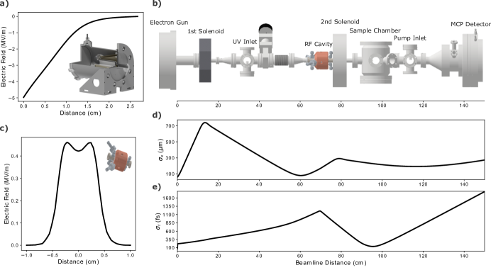
Fig. 1 shows a schematic of the GARUDA electron beamline. The UED pump and probe pulses originate from a 1030 nm, 180 fs FWHM Yb-based PharosTM laser system with 10 W of average power and repetition rate up to 20 kHz. A pulse picker allows for tuning the repetition rate from the regenerative amplifier. The output is routed to a beam-splitter that separates the pulses into pump and probe paths. The pump is directed into an optical parametric amplifier (OPA) to obtain a wavelength-tunable output in the optical to infrared range of the electromagnetic spectrum. This laser pulse is then free space-coupled into a vacuum chamber housing the sample to provide an impulsive excitation that rapidly drives the sample away from equilibrium. On the other path, the probe is frequency-doubled twice via nonlinear crystals to provide 257.5 nm (4.8 eV) laser pulses. This pulse is then focused to a 60 m spot on an in-vacuum poly-crystalline Cu cathode where it releases an electron bunch via the photoelectric effect. Increasing bunch charge provides improved diffraction signal to noise at the cost of greater transverse and longitudinal broadening. The compromise between these effects must be weighed carefully in selecting an operating bunch charge. The data shown here is all collected at 1 fC bunch charge.
The electron bunch is then accelerated to 40.4 kV kinetic energy by a DC field that over the cathode/anode 11 mm gap brings their velocity (normalized to the speed of light) to . Initially, the transverse and longitudinal size of the electron pulse grow rapidly due to the non-zero thermal emittance and the mutual Coulomb repulsion (space charge). A solenoid magnetic lens directly after the gun is used to control the transverse profile of the beam and focus it into the entrance of the RF compression cavity. At the appropriate RF cavity phase, the electron pulse is given a negative chirp with no net impulse. Consequently, the mean velocity of the beam remains constant, but electrons at the back (front) of the pulse are accelerated (decelerated). Thus, the pulse will come to a longitudinal focus at some distance after the RF compression cavity which, at the ideal RF power and phase, will be the sample plane, in this case 27.9 cm downstream of the RF cavity.
When the cavity is set at the longitudinally focusing phase, the RF field has a defocusing effect on the transverse beam profile. A 2nd solenoid refocuses the beam to a transverse size () of approximately 200 m at the sample plane. This is illustrated in Fig. 1(d). Here there is a trade-off between spot-size on the sample and Q-space resolution on the detector. In order to achieve a smaller sample plane spot-size, there is also a retractable 100 m diameter pinhole directly before the sample which allows for more control on the spot-size for the experiments at the cost of decreased intensity.
II.2 Beamline Simulation
We utilize the General Particle Tracer (GPT) software package to simulate the propagation of electron bunches along the beamline. GPT is a three dimensional particle tracking software that numerically simulates charged particle dynamics in external electromagnetic fields while accounting for space charge effects [20]. Fig. 1 (c) & (d) show the simulated transverse () and temporal () bunch widths as a function of the average position along the beamline.
In this simulation, the RF cavity phase and power are optimized to longitudinally focus on the sample plane while imparting no net impulse to the electron bunch; we will refer to these optimized values as the ideal RF phase and RF amplitude. If we were to vary the RF phase away from this ideal value, would grow until it reaches a maximum expansion phase at 90 degrees away from the compression phase. Similarly, if we were to vary the RF power while sitting at the focusing phase, the electron bunch would come to a longitudinal focus either before or after the sample plane. Fig. 2 shows a simulated mapping of at the sample plane as a function of RF amplitude and phase. For fixed RF powers below the ideal level, the minimizing phase always corresponds to the zero field crossing where the field slope is maximal. However for RF power levels higher than ideal, the minimizing phase along cuts of constant RF power bifurcates into two branches. In these branches, either a net acceleration or deceleration is applied to the electron bunch along with the longitudinal compression; the shift away from the zero field crossing exposes the electron bunch to a weaker field slope which compensates for the excess power thus holding the focus at the sample plane.
These two bifurcated branches achieve similar simulated compared to the ideal condition; however, arrival time jitter is significantly worse along the branches. At the ideal condition, the zero field crossing completely eliminates first order arrival time jitter effects due to fluctuations in the RF power; however, in the high power branches, this arrival time jitter increases more than tenfold to a level of 40 fs per 0.1 % power variation in the cavity. Additionally, the dependence of on RF phase is more severe in the high power branches compared to the ideal condition. Hence, operating in these branches is undesirable.
It is important to consider the effects of RF compression on the momentum resolution in a UED measurement. The chirp applied by the RF cavity necessarily broadens the energy distribution of the electron bunch. The angle at which electrons diffract for a given in reciprocal space is inversely proportional to the incident electron momentum; thus, the relative spread in incident energy translates to a corresponding relative spread in diffracted angles. In other words
where is the root-mean-square (rms) broadening in reciprocal space and is the rms spread in electron momentum. As a numerical example, we consider the (100) peak of 1-TaS2 which has a momentum transfer of Å-1. From GPT simulation, the energy spread after the RF cavity is which yields Å-1 for the resolution in reciprocal space.
This degradation of resolution is entirely negligible compared to the resolution limits associated with the beam emittance. The latter can be estimated
where is the rms divergence at the sample. This gives 1.8 Å-1 of broadening per degree of rms beam divergence; from GPT simulation, the spread in angles at the sample plane is roughly 0.06∘. Thus, we have 0.1 Å-1 of resolution broadening just from the range of angles within the bunch. In principle this could be improved by using a larger spot size at the sample or a smaller beam emittance, but it is still orders of magnitude larger than the broadening due to the beam energy spread imparted by the RF cavity.
II.3 RF cavity and cooling
A single-cell S-band 2.856 GHz buncher cavity constructed by Radiabeam technologies (Fig. 3) based on a re-entrant nose cone geometry is used to impart the required RF kick to the beam. The conversion of RF cavity power into beam kinetic energy is quantified by the shunt impedance ; this relates the power fed into the cavity to the peak accelerating voltage as:
| (5) |
The re-entrant geometry is designed to obtain a cavity shunt impedance of 3.3 M so that 3 W of RF power is sufficient to reach the nominal cavity voltage of 3 kV. The distance between the nose cones is carefully chosen so that 40 keV electrons will enter and exit the cavity in half a cycle of the RF fields in order to maximize the transit time factor.
The cavity is equipped with two n-type ports, one of which is used to feed the input coupler into the cavity and the other is used for a probe antenna, calibrated to -12 dB coupling to monitor amplitude and phase of the RF fields.
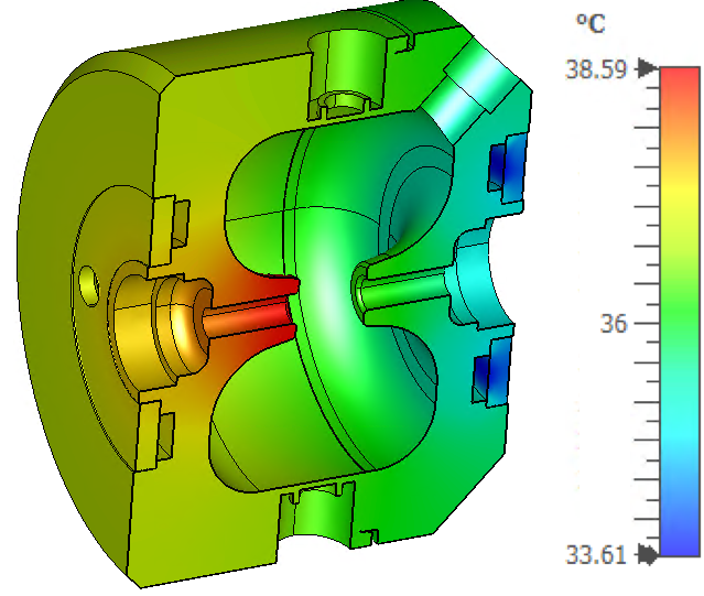
When operating in CW mode, the maximum power into the cavity is limited by heat transfer considerations. Two separate water cooling circuits can be used to control the temperature of the copper structure, but due to a leaky connection, in this initial phase we have operated using only the upstream water channels. (see left in Fig. 3). Although not ideal, heat load simulations indicate this mode of operation is feasible as it yields a relatively modest peak temperature increase of less than 5∘C under 50 W of input power and the expected operating input power is less than 5 W.
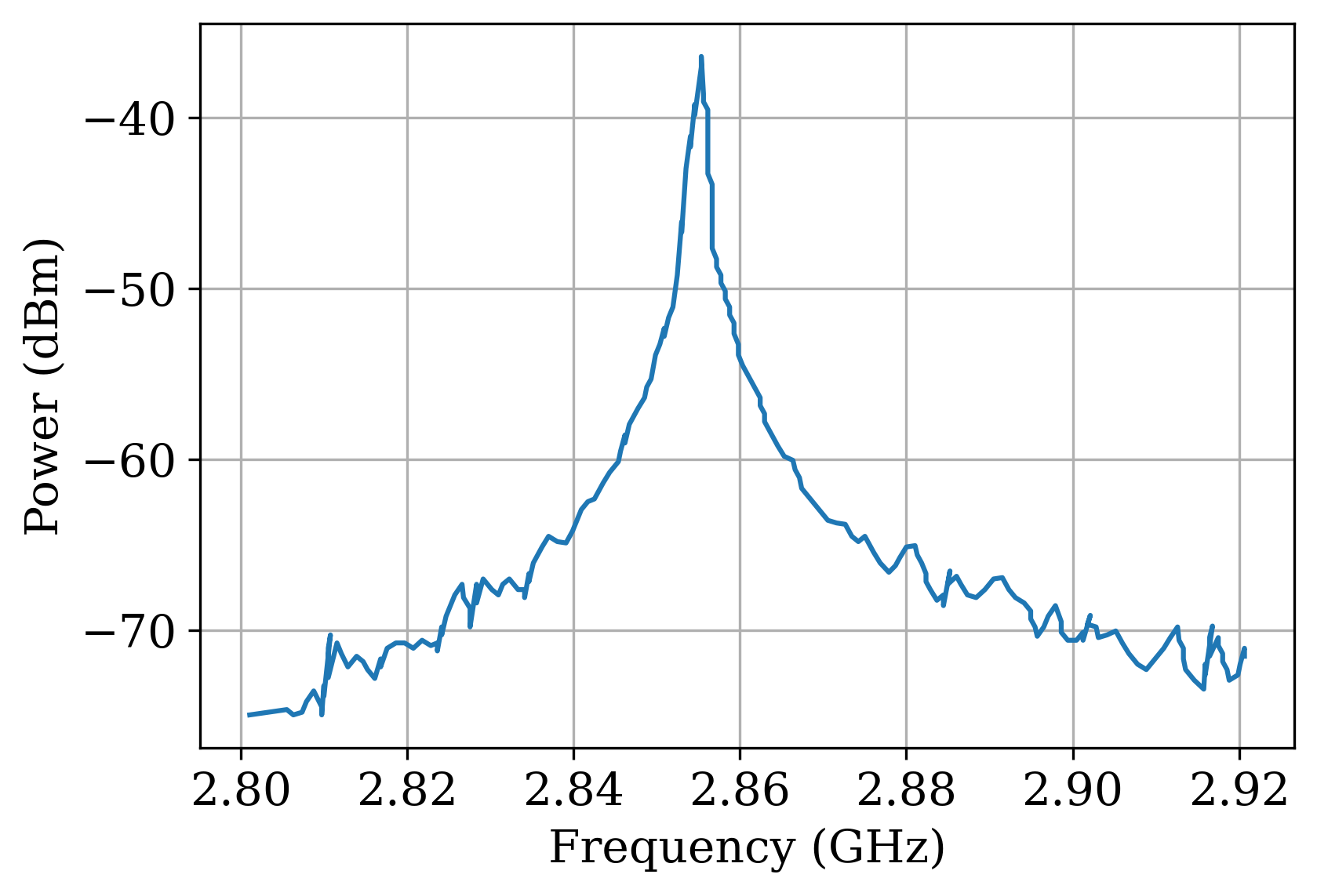
The cavity dimensions are designed such that the resonant frequency is 2.856 GHz to very high accuracy. Mismatches between the cavity resonant frequency and the frequency from the oscillator lead to reflections and losses. The input coupler that converts the RF power from the coaxial cable to the cavity mode has a coupling factor of 0.98 so that the return loss is very small (-40 dB of the input power), as confirmed by the measurement shown in Fig. 3. After tuning and adjustments at UCLA, a sharp cavity resonance with unloaded Q of 12000 in agreement with simulations was measured with a vector network analyzer at 2.856 GHz prior to installation on the beamline (Fig. 3).
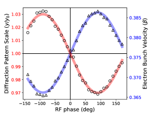
The design shunt impedance is verified by measuring the change in the beam energy/velocity as a function of the RF phase as shown in Fig. 4. The deviation in beam momentum is obtained by monitoring the shift in the Bragg peaks from a gold reference sample as a function of the input phase at an input power of 2.3 W. Acceleration (deceleration) of the electron bunch contracts (expands) the scale of the diffraction pattern on the detector. A sinusoidal fit of this diffraction scale variation with RF phase yields a cavity voltage of 2 kV and a shunt impedance of 3.2 M in excellent agreement with the predictions. Note that this measurement also allows one to easily determine the phase for which no net impulse is imparted to the bunch as described later.
III Synchronization and feedback
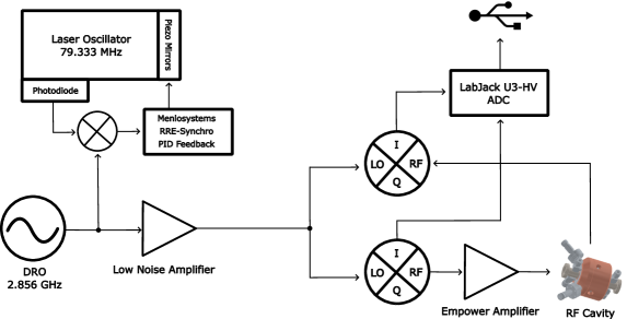
RF compression requires precise synchronization between the electron arrival time at the RF cavity and the phase of the RF field inside the cavity. This synchronization problem is central to state-of-the-art RF technologies at large-scale particle accelerators; thus, there is a large body of knowledge in this domain. In the case of UED experiments at the GARUDA beamline, this problem is addressed by synchronizing the laser oscillator (seed for pump and probe pulses) and the RF cavity wave to a master clock.
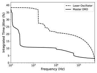
Fig. 5 shows a simple schematic of this system. In order to stabilize the RF compression process, the laser oscillator is locked via PID feedback to a master dielectric resonator oscillator (DRO) providing a low noise electronic signal at 2.856 GHz frequency. The frequency of the laser oscillator cavity is 79.333 MHz; pulses from this oscillator are converted to an electronic signal via a fast photodiode with a bandwidth large enough to resolve the harmonics of the 79.333 MHz pulse train up to the 36th order (2.856 GHz). The DRO signal is mixed with the photodiode to produce an error voltage that measures the phase mismatch and drives two piezo mirrors inside the oscillator to adjust the length of the cavity and synchronize phase to within 50 fs jitter.
The RF cavity is driven by an amplified and phase-shifted signal from this same master DRO. The main amplifier is a fixed gain Empower model 2193 which is run below saturation to allow for amplitude feedback adjustments. The variable attenuation and phase shift is PID feedback controlled by two IQ mixers (in-phase/quadrature). These are four port devices (two ports for RF and two ports for low frequency voltage) which contain two mixers one of which introduces a phase shift into the signal by 90 degrees.
If the following two signals are applied to the RF ports of the mixer
| (6) | ||||
| (7) |
the IQ mixer will produce two DC voltages, I and Q, such that:
| (8) | ||||
| (9) |
Here, we take as a signal from the master DRO and as a signal from a antenna probe in the RF cavity. The mixer acts to demodulate the signal to the and voltages which yield the relative amplitude and phase of the RF cavity wave. Let ,
| (10) | ||||
| (11) |
Likewise, we can use a separate IQ mixer to set the amplitude and phase for an RF wave applied to port . In this case, the signal is modulated according to the DC voltages externally applied at the and ports of the mixer. With simultaneous operation of two IQ mixers, one acting as a modulator and one acting as a demodulator, we can measure and directly control the phase and amplitude of the RF field inside the cavity.
Prior to deployment in the feedback system, the IQ mixers must be calibrated. This is accomplished using a 2-port vector network analyzer (VNA) and an analog phase shifter. Ideally, the relationship between the true phase (as measured by the VNA) and the IQ mixers set-phases would be a line with unity slope. In practice, there can be a deviation from this linearity due to a variety of possible causes including the response of the antenna inside the cavity and the actual response of the mixers themselves.
Let (, ) and (, ) denote the voltages on the modulation and demodulation mixers respectively. We can convert these voltages to amplitudes and phases through equations 10 and 11 to obtain modulation parameters (, ), and the actual demodulated amplitude and phase in the cavity (, ). For feedback on the RF phase and amplitude, we require a mapping from (, ) to (, ) which will have a similar form to the analytic mapping with some non negligible deviations due to the non-linear response and thresholds of the Empower amplifier. To correct for these, we use a lookup table approach. The demodulated values of amplitude and phase are measured for a dense grid of input modulation parameters; this discrete mapping is then interpolated to create a continuous function (, ) (, ). An example of this mapping is shown in Fig. 7 and clearly shows an approximate correspondence to the expected conical and arc-tangent behavior.

A LabJack U3-HV with a LJTick-DAC is used to digitally read and write the IQ mixers’ DC voltages; this device provides a -10 to 10 V range. The read and write DC voltages for the IQ mixers are typically low (around 0.5 V) and voltage dividers and amplifiers are used to boost the signal to fill the dynamic range of the LabJack.
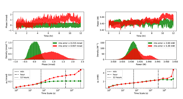
UED experiments at the GARUDA beamline frequently require 12 hours of data acquisition to achieve high quality signal to noise. During this time, the same UED trace is scanned over many times and the results are averaged. Fig. 8 displays RF amplitude and phase data over two separate 12 hour periods contrasting the stability without feedback to the stability with feedback. It is apparent that the feedback results in a significant improvement of phase stability on timescales as short as 1 hour while the improvement in amplitude stability (more than a factor of two) takes longer to appreciate.
Note that it is very important to feedback on the amplitude in the IQ mixer based system. We can imagine running feedback in which amplitude is unconstrained but phase is continuously corrected; in this scenario, the phase feedback would actually add significant noise into the amplitude trace due to the cross-talk in the lookup table . The two quantities must be fed-back on simultaneously for best performance when using the mixers. Given the measured performances of the feedback on in Fig. 8, we can estimate for this data set the time-zero jitter due to fluctuations in RF cavity phase and power to be lower than 20 fs at the zero-field crossing.
IV System Characterization
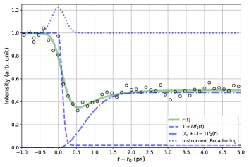
The temporal resolution of the system is characterized through measurements of the charge-density-wave (CDW) dynamics of the compound 1-TaS2. This is a widely studied quasi-two-dimensional compound belonging to the transition metal dichalcogenide family of materials. It is metallic at high temperatures (550K), but below this it hosts a series of phase transitions through different CDW states of varying characteristic wavevectors [21, 22]. Here, we present UED measurements on the photo-induced transition from the room temperature nearly-commensurate charge-density-wave (NCCDW) to the incommensurate charge-density wave (ICCDW). Time-resolved x-ray diffraction studies on this transition have shown a complete suppression of the NCCDW peaks within 400 fs of pump excitation followed by a slight recovery [23]. This time-resolved x-ray diffraction data provides a measure of the intrinsic response time of the photo-induced NCCDW to ICCDW transition. We utilize a phenomenological function calibrated to this response time as an effective Green’s function for the system describing the intensity of the NCCDW diffraction peak as a function of time in the limit of zero instrument broadening.
Here defines the magnitude of the initial intensity drop, and is the intensity in the limit of . The intrinsic timescales calibrated from the time-resolved x-ray diffraction of Laulhé et al. are taken as fs and fs, where the former controls the speed of the initial drop in intensity and the latter controls the recovery.
Our data is fit to a convolution of this Green’s function with a Gaussian of variance to represent the instrument broadening. Thus, the fit curve is given by,
| (12) |
Fig. 9 shows a fit of to UED data on the photo-induced NCCDW to ICCDW transition. The data was collected at optimized RF power and RF phase; thus, the value of extracted from this curve is the minimum achieved instrument response time: 182 fs. This quantity contains all sources of instrument broadening; however, the width of the IR pump ( fs), the width of the electron probe pulse (), and the arrival time jitter () are the dominant factors. By subtracting in quadrature the length of the laser pump pulse and the contribution of the timing jitter (50 fs) we obtain an estimate for the electron bunch temporal width which is in excellent agreement with the prediction of the particle tracking simulations fs.
To empirically determine the operating phase for the RF cavity, we rely on the measure of the Bragg peak position as a function of the RF phase at a fixed RF power shown in Fig. 4. The zero crossings of this curve correspond to phases of zero net impulse imparted to the electron beam; this can occur for either a compression phase or an expansion phase that are separated by 90 deg. To differentiate the two, it is necessary to know whether increasing phase leads or lags the RF wave. In our case, phase leads the wave which means that the zero crossing where is the compression phase. The precision of this method is limited by position resolution of the Bragg peaks in the diffraction pattern. Using Gaussian fits for the peak profiles allow sub-pixel accuracy in the determination of their centroids; nevertheless, the measurement of the compression phase is still uncertain to within a few degrees.
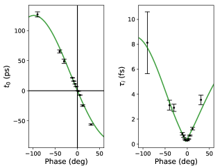
Significantly better precision on the compression phase determination is obtained from time-zero measurements in a UED experiment. Time-zero is defined here as where and are the mean arrival times at the sample of the probe (electrons) and pump (IR laser) respectively. In practice, the arrival time of the pump is varied with a delay stage and the delay stage position corresponding to is measured from fitting the time trace as shown in Fig. 9. By taking a reference time-trace in which no power is supplied to the RF cavity, one can calibrate the delay stage position that corresponds to . Then, arrival time variations due to the RF field can be measured to within fs precision near the compression phase.
Fig. 10 shows results from UED data collected at a fixed RF power for a large number of RF phases. The extracted values of are measured in reference to a UED time trace in which the RF cavity was off; hence, the phase for which is a condition in which the RF field imparts zero net impulse to the electron beam. Again there are two phases that satisfy this condition: a compression phase and an expansion phase. The zero crossing where is the ideal RF compression phase. This method measures the compression phase with excellent precision on the order of 1 mrad (0.057 deg). The slope of the at the zero crossing is measured to be -1.54 ps/deg in good agreement with the prediction from Eq. 4.
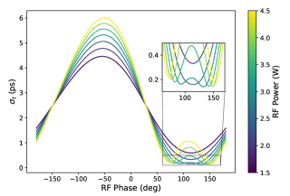
The dependence of the system response time on phase at the ideal RF power is also given in Fig. 10. The range of compressing phases at the ideal power is quite large; however, the onset of time-zero jitter due to RF power fluctuations can quickly increase the system response time as phase is moved away from the zero-field crossing. For the data presented in Fig. 10, the total RF power jitter was 200 mW; however, the phase jitter was held below 0.5 mrad. Even with this comparatively high jitter in RF power, the system response time at the zero-field crossing is still below 200 fs. As shown in Figure 8, the RF power jitter has since been improved to the 2.6 mW level.
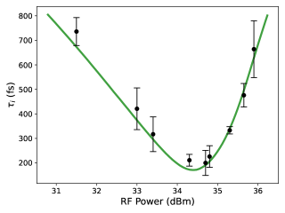
Fig. 11 displays measurements of the system response time at various RF powers while the phase is set at the zero crossing. This corresponds to varying the focal length of the RF longitudinal lens. Clearly, a power that is too high (low) yields a focus before (after) the sample plane. This data is found to be in good agreement with the expected curve from particle tracking simulation and shows a relatively large, approximately 300 mW range, for an acceptable temporal focus below 200 fs.
V Conclusions
In conclusion, a novel UED beamline operating in CW mode at 40.4 kV electron energy has been commissioned at UCLA based on RF compression to obtain a temporal resolution below 200 fs. The cavity is operated in CW mode allowing for fast feedback control. A vector-based feedback loop using IQ mixers to read out and write amplitude and phase of the RF field in the cavity is implemented. Further improvements in temporal resolution can be obtained increasing the energy from the gun (currently limited by arcing at the cathode) and optimizing the compression for different bunch charges. Compression of the pump laser pulse and reduction of the RF cavity to sample distance would also improve the instrument response time. There are also possible advances in which timing jitter is handled through post processing. Since the UED scans are performed stroboscopically, good resolution electronic measurements could enable a scheme in which each probe shot is assigned its own arrival time and machine learning/artifical intelligence is used to compensate for the residual timing jitter [24].
Acknowledgements.
This work was supported by the U.S. Department of Energy (DOE), Office of Science, Office of Basic Energy Sciences under Award No. DE-SC0023017, the National Science Foundation under Grant No. DMR-1548924 and NSF MRI grant 1828705. We would also like to thank Nathan Burger, Amir Amhaz, Kirill Talesky, Alexander Ody, Shiying Wang, Mikhael Rasiah and Jayanti Higgins for their help on various aspects of the beamline construction. The data that support the findings of this study are available from the corresponding author upon reasonable request.References
- Mourou and Williamson [1982] G. Mourou and S. Williamson, Picosecond electron diffraction, Applied Physics Letters 41, 44 (1982).
- Zewail [2006] A. H. Zewail, 4d ultrafast electron diffraction, crystallography, and microscopy, Annu. Rev. Phys. Chem. 57, 65 (2006).
- Sciaini and Miller [2011] G. Sciaini and R. D. Miller, Femtosecond electron diffraction: heralding the era of atomically resolved dynamics, Reports on Progress in Physics 74, 096101 (2011).
- Filippetto et al. [2022] D. Filippetto, P. Musumeci, R. Li, B. J. Siwick, M. Otto, M. Centurion, and J. Nunes, Ultrafast electron diffraction: Visualizing dynamic states of matter, Reviews of Modern Physics 94, 045004 (2022).
- Van Oudheusden et al. [2007] T. Van Oudheusden, E. De Jong, S. Van der Geer, W. t Root, O. Luiten, and B. Siwick, Electron source concept for single-shot sub-100 fs electron diffraction in the 100 kev range, Journal of Applied Physics 102 (2007).
- Van Oudheusden et al. [2010] T. Van Oudheusden, P. Pasmans, S. Van Der Geer, M. De Loos, M. Van Der Wiel, and O. Luiten, Compression of subrelativistic space-charge-dominated electron bunches for single-shot femtosecond electron diffraction, Physical review letters 105, 264801 (2010).
- Qi et al. [2020] F. Qi, Z. Ma, L. Zhao, Y. Cheng, W. Jiang, C. Lu, T. Jiang, D. Qian, Z. Wang, W. Zhang, et al., Breaking 50 femtosecond resolution barrier in mev ultrafast electron diffraction with a double bend achromat compressor, Physical review letters 124, 134803 (2020).
- Kim et al. [2020] H. W. Kim, N. A. Vinokurov, I. H. Baek, K. Y. Oang, M. H. Kim, Y. C. Kim, K.-H. Jang, K. Lee, S. H. Park, S. Park, et al., Towards jitter-free ultrafast electron diffraction technology, Nature photonics 14, 245 (2020).
- Li et al. [2022] W. Li, C. Duncan, M. Andorf, A. Bartnik, E. Bianco, L. Cultrera, A. Galdi, M. Gordon, M. Kaemingk, C. Pennington, et al., A kiloelectron-volt ultrafast electron micro-diffraction apparatus using low emittance semiconductor photocathodes, Structural Dynamics 9 (2022).
- Scoby et al. [2010] C. Scoby, P. Musumeci, J. Moody, and M. Gutierrez, Electro-optic sampling at 90 degree interaction geometry for time-of-arrival stamping of ultrafast relativistic electron diffraction, Physical Review Special Topics-Accelerators and Beams 13, 022801 (2010).
- Zhao et al. [2018] L. Zhao, Z. Wang, C. Lu, R. Wang, C. Hu, P. Wang, J. Qi, T. Jiang, S. Liu, Z. Ma, et al., Terahertz streaking of few-femtosecond relativistic electron beams, Physical Review X 8, 021061 (2018).
- Weathersby et al. [2015] S. Weathersby, G. Brown, M. Centurion, T. Chase, R. Coffee, J. Corbett, J. Eichner, J. Frisch, A. Fry, M. Gühr, et al., Mega-electron-volt ultrafast electron diffraction at slac national accelerator laboratory, Review of Scientific Instruments 86 (2015).
- Siddiqui et al. [2023] K. Siddiqui, D. Durham, F. Cropp, F. Ji, S. Paiagua, C. Ophus, N. Andresen, L. Jin, J. Wu, S. Wang, et al., Relativistic ultrafast electron diffraction at high repetition rates, arXiv preprint arXiv:2306.04900 (2023).
- Zhu et al. [2015] P. Zhu, Y. Zhu, Y. Hidaka, L. Wu, J. Cao, H. Berger, J. Geck, R. Kraus, S. Pjerov, Y. Shen, et al., Femtosecond time-resolved mev electron diffraction, New Journal of Physics 17, 063004 (2015).
- Chatelain et al. [2012] R. P. Chatelain, V. R. Morrison, C. Godbout, and B. J. Siwick, Ultrafast electron diffraction with radio-frequency compressed electron pulses, Applied Physics Letters 101 (2012).
- Xiong et al. [2020] Y. Xiong, K. J. Wilkin, and M. Centurion, High-resolution movies of molecular rotational dynamics captured with ultrafast electron diffraction, Physical Review Research 2, 043064 (2020).
- Otto et al. [2017] M. R. Otto, L. René de Cotret, M. J. Stern, and B. J. Siwick, Solving the jitter problem in microwave compressed ultrafast electron diffraction instruments: Robust sub-50 fs cavity-laser phase stabilization, Structural Dynamics 4 (2017).
- Pasmans et al. [2013] P. Pasmans, G. van den Ham, S. Dal Conte, S. van der Geer, and O. Luiten, Microwave tm010 cavities as versatile 4d electron optical elements, Ultramicroscopy 127, 19 (2013).
- Denham and Musumeci [2021] P. Denham and P. Musumeci, Analytical scaling laws for radiofrequency based pulse compression in ultrafast electron diffraction beamlines, arXiv preprint arXiv:2106.02102 (2021).
- De Loos and der Geer [1996] M. De Loos and V. der Geer, General particle tracer: A new 3d code for accelerator and beamline design, 5th European Particle Accelerator Conference , 1241 (1996).
- Salvo and Graebner [1977] F. D. Salvo and J. Graebner, The low temperature electrical properties of 1T-TaS2, Solid State Communications 23 (1977).
- Fazekas [1979] P. Fazekas, Electrical, structural and magnetic properties of pure and doped 1T-TaS2, Philosophical Magazine B 39 (1979).
- Laulhé et al. [2017] C. Laulhé, T. Huber, G. Lantz, A. Ferrer, S. O. Mariager, S. Grübel, J. Rittmann, J. A. Johnson, V. Esposito, A. Lübcke, L. Huber, M. Kubli, M. Savoini, V. L. R. Jacques, L. Cario, B. Corraze, E. Janod, G. Ingold, P. Beaud, S. L. Johnson, and S. Ravy, Ultrafast formation of a charge density wave state in 1T-TaS2: Observation at nanometer scales using time-resolved x-ray diffraction, Phys. Rev. Lett. 118 (2017).
- Cropp et al. [2023] F. Cropp, L. Moos, A. Scheinker, A. Gilardi, D. Wang, S. Paiagua, C. Serrano, P. Musumeci, and D. Filippetto, Virtual-diagnostic-based time stamping for ultrafast electron diffraction, Physical Review Accelerators and Beams 26, 052801 (2023).
- De Loos et al. [1996] M. De Loos, S. Van der Geer, et al., General particle tracer: A new 3d code for accelerator and beamline design, in 5th European Particle Accelerator Conference, Vol. 1241 (1996).
- F. Zhou et al. [2015] J. C. S. F. Zhou, E. J. T. Vecchione, J. C. A. Brachmann, and S. W. S. Gilevich, Establishing reliable good initial quantum efficiency and in-situ laser cleaning for the copper cathodes in the rf gun, Nuclear Instruments and Methods in Physics Research Section A 783 (2015).