FHEmem: A Processing In-Memory Accelerator for Fully Homomorphic Encryption
Abstract
Fully Homomorphic Encryption (FHE) is a technique that allows arbitrary computations to be performed on encrypted data without the need for decryption, making it ideal for securing many emerging applications. However, FHE computation is significantly slower than computation on plain data due to the increase in data size after encryption. Processing In-Memory (PIM) is a promising technology that can accelerate data-intensive workloads with extensive parallelism. However, FHE is challenging for PIM acceleration due to the long-bitwidth multiplications and complex data movements involved. We propose a PIM-based FHE accelerator, FHEmem, which exploits a novel processing in-memory architecture to achieve high-throughput and efficient acceleration for FHE. We propose an optimized end-to-end processing flow, from low-level hardware processing to high-level application mapping, that fully exploits the high throughput of FHEmem hardware. Our evaluation shows FHEmem achieves significant speedup and efficiency improvement over state-of-the-art FHE accelerators.
Index Terms:
Cryptography, Processing In-Memory, Domain-Specific AccelerationI Introduction
The data explosion leads to an increasing trend of cloud-based outsourcing. Extensive outsourcing significantly increases the risk of sensitive data leaking, necessitating data encryption for protection. Fully homomorphic encryption (FHE) is an emerging technology that enables computations on encrypted data without user interference [1, 2, 3, 4]. FHE provides end-to-end data security during the outsourcing, including data transfer and computation, without any requirements for the underlying system and hardware. However, FHE is several orders of magnitude slower than plain data while requiring a large memory footprint [5, 6, 7, 8, 9]. The inefficiency of FHE results from the data and computation explosion after encryption. Even though FHE can encrypt a vector into a single ciphertext [2, 4], the ciphertext size is still large and includes two or more high-degree polynomials (e.g., ) with long-bit coefficients (e.g., 1000 bits).
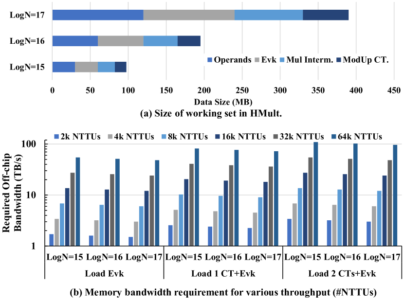
Such issues motivate researchers to develop customized accelerators that provide 4 orders of magnitude speedup over conventional systems [5, 6, 7, 8, 9]. However, existing accelerators are still significantly bounded by the data movement even with large and costly on-chip scratchpads [5, 8, 6]. As shown in Figure 1(a), each homomorphic multiplication () requires to working set for to . In Figure 1(b), we follow the method in previous work [5] to analyze the memory bandwidth required by different numbers of number theory transform units (NTTUs) under 3 data loading scenarios during a holomorphic operation with key-switching operation (KSO) which is the most expensive FHE primitive. Our investigation shows simply doubling the throughput of existing accelerators (1K to 2K) may require over 3TB/s of off-chip bandwidth. Previous accelerators adopt large on-chip storage, up to 512MB, to hold the large working set of FHE computation. However, large on-chip storage can still suffer from frequent off-chip data transfers due to cache misses on extensive FHE data. Therefore, it is challenging to achieve both high compute throughput and high memory bandwidth on conventional architectures for FHE applications.
In this work, we exploit the processing in memory (PIM) acceleration for FHE, which is promising to support extensive parallelism with high internal memory bandwidth [10, 11, 12, 13, 14, 15, 9]. There are several types of PIM architectures that support PIM in different levels in the memory architecture, including subarray-level [14, 10, 13], bank-level [16, 17], and channel-level [18]. These PIM technologies adopt high-throughput processing elements that fully exploit the internal memory links that provide higher bandwidth than the off-chip data path. Even though the high parallelism and bandwidth of PIM potentially fit the data-intensive parallel computations of FHE, there exist several challenges that existing PIM-based architectures cannot easily solve. First, FHE works on high-degree polynomials with long-bit coefficients and is multiplication-intensive. Such long-bit multiplication is challenging to all existing PIM technologies. For near-bank PIM, the throughput is limited by bank IO width. Furthermore, even though the bank-level PIM can adopt highly efficient multipliers, reading the data from the memory cells is still energy-consuming. The bit-serial subarray-level PIM can exploit a significantly large number of internal links (e.g., bitlines). However, the number of operations required by subarray-level PIM may increase quadratically with the operand bit-length. These energy-consuming operations run in a lock-step manner, significantly increasing delay and energy. Our evaluation shows such PIM technologies fail to provide comparable throughput and energy efficiency to the state-of-the-art FHE accelerators (Section II-D). Integrating more functionality in the sense amplifiers can solve the problem, but introducing significant modifications in conventional DRAM structures [10]. The second challenge of PIM acceleration for FHE is the complex data movement patterns, including the base conversion and number theoretic transform (NTT), that the existing memory architecture cannot efficiently support.
To tackle these challenges, we propose FHEmem, an accelerator based on a novel high-bandwidth memory (HBM) architecture optimized for the efficiency of processing FHE operations. FHEmem introduces a novel near-mat processing architecture, which integrates compute logic near each mat without changing the area-optimized mat architecture. FHEmem exploits the existing intra-memory data links, with careful extensions based on the practicability, to enable efficient in-memory processing of various challenging FHE operations. Furthermore, we propose a software-level framework to map FHE programs onto FHEmem hardware. We propose a load-save pipeline that can fully utilize the memory for FHE programs to support high-throughput computing with minimum data loading overhead.
We summarize the contributions of this work as follows:
-
•
We propose an FHE accelerator with a novel near-mat processing that supports high-throughput and energy-efficient in-memory operations. Our design efficiently exploits the existing data paths with practical modifications in DRAM that introduce relatively lightweight overhead compared to prior high-throughput PIM solutions.
-
•
We propose an FHE mapping framework that generates a load-save pipeline and data layout that maximizes the utilization of FHEmem for general FHE programs.
- •
II Background and Motivation
II-A Fully Homomorphic Encryption
We focus on CKKS scheme [2] which is widely used in many application domains because it supports real numbers and SIMD packing [19, 20, 21].
Basics of CKKS: We define the polynomial ring , where is power of 2. We denote for residue ring of modulo an integer . The ecurity parameter sets the ring size and a ciphertext modulus . For each plaintext message, , encryption Encrypt() generates a ciphertext , where , is uniformly sampled from , and and are sampled from a key/error distribution respectively. Each ciphertext can pack up to real numbers to support SIMD processing on all packed numbers [4, 2]. The original modulus of a ciphertext decreases with homomorphic multiplications by a rescaling process that reduces the modulus by a each time. Therefore, CKKS is a leveled homomorphic scheme that only supports levels of multiplications for each ciphertext. The technique to recover the ciphertext level is bootstrapping [22].
Arithmetic Operation: Given two ciphertexts , where is the modulus at level , the polynomial operation can homomorphically evaluate the arithmetic for plaintexts. The homomorphic multiplication (HMul) between two ciphertexts is complex: , where is encrypted under the secret key . This requires a re-linearization operation with an expensive key-switching process on (Section II-A). The rescaling is applied during the relinearlization, using the divide and round operation: ReScale to rescale the ciphertext as well as the modulus.
Rotation: CKKS supports homomorphic rotation which rotates the plaintext vector by an arbitrary step. The rotation is implemented by Galois group automorphism [23] which consists of mapping on each coefficient : ,where is an odd integer satisfying and if ( otherwise). Each automorphism implements a Rotate which rotates the plaintext by . Each automorphism also requires a KeySwitch after each Rotate.
NTT and Residue Number System: Number Theoretic Transform (NTT) is a widely used technique to optimize polynomial multiplications. NTT transforms two input polynomials of a multiplication, and , to NTT(a) and NTT(b). We can calculate , where denotes element-wise multiplication with complexity, where is the polynomial degree. An inverse NTT (iNTT) can transform . The complexity of NTT and iNTT is , faster than the original polynomial multiplication with complexity. Residue number system (RNS) is a technique that avoids computation on large values. We adopt the full-RNS version of CKKS [24]. For polynomials in , the scheme chooses a set of pair-wise coprime integers where and . Each polynomial is represented by polynomials , where . We can evaluate FUNC by independently calculating FUNC based on Chinese Remainder Theorem. These RNS moduli are also used as the leveled modulus, so each multiplication removes one RNS polynomial in the ciphertext.
Key Switching: Key switching is the most expensive high-level operation in CKKS, where we use the state-of-the-art generalized key switching algorithm [22]. The key of key switching is the multiplication between the input ciphertext and the evaluation key . However, the naive multiplication will cause the overflow on modulus . To avoid overflow on modulus , has a larger modulus with the special modulus . Thus the first step is to convert with modulus into a ciphertext with by a base conversion (BConv):
| (1) |
BConv requires the data in the original coefficient domain. We need to apply an iNTT on the data before BConv. BConv features an all-to-all reduction between different and residual polynomials. We convert the BConv result back to the NTT domain to efficiently process the multiplication with . The algorithm converts the result with modulus back to modulus using BConv. Recent advanced CKKS schemes exploit a configurable value to factorize the modulus into moduli to increase higher multiplication level [22].
II-B Memory Issues of FHE Accelerators
FHE features large polynomial operations and complex data dependency caused by (i)NTT and BConv. Recent works [25, 5, 6, 7, 8, 9] have proposed customized accelerators for FHE. Even though these accelerators achieve up to 4 orders of magnitude speedup over CPUs, they suffer from limited memory bandwidth. For example, previous work [5] observed that the excessive usage of high-throughput function units might be a waste - it would be cost-efficient to determine the throughput of on-chip processing elements based on the available memory bandwidth. Such memory issues result from the large data size required for each FHE operation. Existing FHE accelerators adopt large on-chip storage (180MB for SHARP [8], 256MB for CraterLake [6], and 512MB for BTS [5]/ARK [7]) to reduce the frequent off-chip data loading. However, such large on-chip storage may still be insufficient for FHE, as shown in Figure 1. For large FHE parameter settings, on-chip storage may only store working sets of one or two , leading to frequent off-chip data loading when locality is low. The analysis in Figure 1(b) shows 2k NTTUs require at least 1.5TB/s when only loading , and the bandwidth requirement goes up to 3TB/s when the accelerator needs to load both and two operands. 3TB/s is expected to require 3 HBM3 stacks [26]. If we increase the throughput to 64k NTTUs, which can fully parallelize operations for , the bandwidth requirement can be as high as . Considering it is challenging to significantly increase either the memory bandwidth or the on-chip storage, processing in memory can be a promising alternative.
II-C In-DRAM PIM Technologies
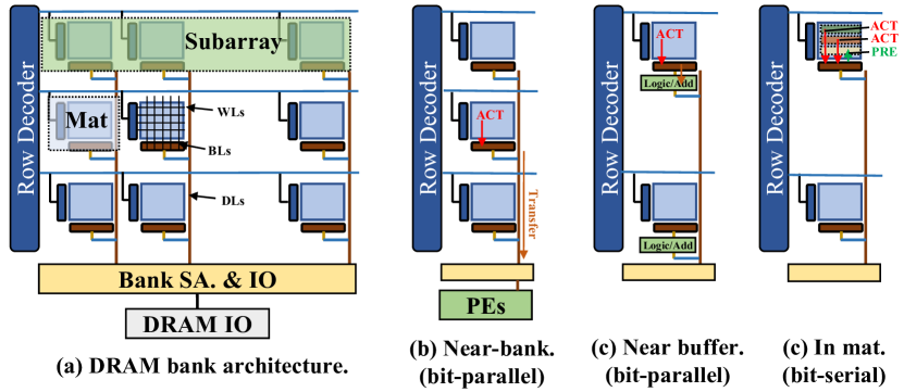
This work focuses on DRAM-based PIM technologies which support larger capacity than SRAM [12] and lower latency than non-volatile memories [11]. Figure 2(a) shows a DRAM bank, which is the basic hardware component in DRAM. A bank consists of 2D cell arrays and peripherals to transfer data between DRAM cells and IOs. The memory cells are grouped into subarrays, each consisting of a row of mats. Each mat has local sense amplifiers (row buffers) sensing a horizontal wordline (WL) through a set of vertical bitlines (BLs). Sense amplifiers in mats of a subarray form the subarray row buffer. Upon receiving access, the bank activates corresponding WL in subarray row buffer and transfers the whole WL to bank-level sense amplifiers via data lines (DLs).
Several DRAM-based PIM technologies support operations in different levels of DRAM architecture. The first technology is near-bank processing, which integrates processing elements (e.g., vector ALUs, RISC-V processor, etc.) near the bank SA and IO [16]. Each bank-level PE is customized to fully utilize the data link bandwidth for processing. PEs in different banks run in parallel to fully utilize the internal bandwidth in DRAM. The second type of PIM augments the subarray sense amplifiers (row buffers) with compute logic [10]. Due to the constrained chip area, the near-buffer PIM only adopts logic gates, full adders, and shift circuits for multi-bit operations. Compared to near-bank processing, near-buffer PIM supports wider input (e.g., 8192b vs. 256b) and can exploit the subarray-level parallelism [27]. These two types of PIM work on the data with a horizontal layout where each data is stored across multiple BLs in a WL. The third type of PIM uses a vertical bit-serial scheme that lays out each data in different WLs of a BL [14]. The bit-serial PIM directly generates the result of computation between different WLs by exploiting the charge-sharing effect of the DRAM mechanism. Such in-mat bit-serial processing does not introduce significant modifications in DRAM. However, the bit-serial computation is slow and power-consuming where an n-bit multiplication using the bit-serial PIM requires around DRAM activations for 8k values.
II-D Challenges of FHE acceleration using PIM
Even though existing PIM solutions can exploit the large internal DRAM bandwidth for high-throughput computation, FHE is still extremely challenging for PIM acceleration.
II-D1 Long-bit multiplication
As introduced in Section II-A, the basic data structure of FHE is high-degree polynomial, whose coefficient can exceed . The RNS-decomposed polynomials still have at least 28-bit coefficients due to the limitation of modulus selection [6, 2]. As the complexity of PIM multiplication significantly increases as the bit-length increases, PIM (especially bit-serial in-mat) may suffer from long latency and high energy efficiency due to costly row activations and precharges. One way to improve the performance and energy efficiency of PIM is by increasing the aspect-ratio (AR) of DRAM mat [28]. A high AR mat has fewer WLs (rows) and shorter BLs than a low AR mat. Shorter BLs can significantly reduce the latency and energy of activation and precharge. For instance, ARx4 mat (128 rows) has half the cycle and consumes 33% less energy than ARx1 mat (512 rows) [28, 10]. Furthermore, increasing the AR also increases the number of subarrays in a bank, leading to a higher degree of parallelism. The downside of high AR is the large area overhead caused by more sense amplifiers and peripherals.
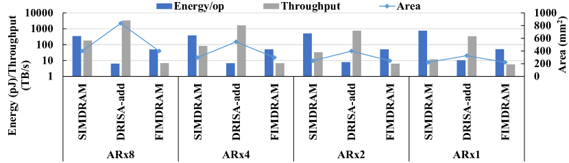
Figure 3 shows the throughput and energy efficiency of different PIM technologies for 32-bit multiplications on a 32GB HBM2E-based architecture (Section V). We evaluate three existing PIM architectures, FIMDRAM [16], DRISA [10], and SIMDRAM [14], that represent near-bank, near-buffer, and in-mat bit-serial PIM respectively. The result shows FIMDRAM and SIMDRAM provide 6.8TB/sand 180.6TB/s throughput while consuming 49.8pJ and 342.9pJ energy for each operation using ARx8 memory. As a reference, the recent FHE accelerator [6], which adopts 150k 28b multipliers, can provide 1PB/s of peak throughput while consuming only 4.1pJ for each multiplication, indicating both FIMDRAM and SIMDRAM are not promising for FHE. DRISA [10] provides over 3PB/s throughput and consumes 6.32pJ for each operation in ARx8 architecture. However, DRISA [10] requires a significant change in the DRAM architecture, incurring around 100% area overhead in high-AR architectures. Furthermore, manufacturing DRISA has significant challenges as the modified sense amplifiers cannot easily be aligned with area-optimized bitlines. To tackle these challenges, FHEmem adopts a novel near-mat processing that integrates compute logic near mat while keeping the mat structure intact, incurring less area overhead than DRISA. Even though the theoretical throughput and energy efficiency of FHEmem are lower than DRISA, our experiments show that higher throughput may not effectively improve the performance due to the data movement (Section V). Overall, FHEmem is a more efficient processing paradigm than prior PIM solutions.
II-D2 Data Transfer Patterns
Another critical challenge of FHE for PIM is the variety of data transfer patterns in different FHE operations. Specifically, the BConv requires the data movement between different RNS polynomials, followed by coefficient-wise operations; (i)NTT and automorphism require data permutation across coefficients of each RNS polynomial. Unfortunately, the conventional memory IO cannot efficiently handle such complex data movement patterns. For BConv, each output RNS polynomial has dependencies with all input RNS polynomials. As each RNS polynomial is large (e.g., 512KB for LogN=64 with 64-bit coefficients), we must distribute RNS polynomials over different memory banks. In conventional memory, such inter-bank data movements take up the shared bus of each channel, leading to significant data movement overhead. For (i)NTT and automorphism, the data movement exhibits a fine-grained pattern within a polynomial. For PIM processing, the coefficient-wise permutation requires permutations between BLs which is not supported in the current memory architecture. FHEmem supports these FHE-specific data transfers efficiently at a relatively low cost by exploiting existing intra-memory data links and adding additional links to the less-dense metal layer in DRAM, without introducing complex permutation networks.
III FHEmem Hardware Architecture
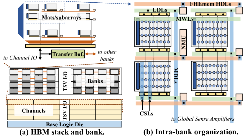
The high-level architecture of FHEmem is based on high-bandwidth memory (HBM), as shown in Figure 4. Specifically, each HBM stack consists of one base die and multiple DRAM dies in a 3D structure. All DRAM dies are divided into multiple channels, each connecting to DRAM part through an independent set of through silicon vias (TSVs). Each channel consists of several banks, and the detailed internal structure of the bank is introduced in Section II-C. FHEmem adopts a new near-mat PIM architecture that modifies the DRAM bank architecture to support high-throughput computations while utilizing available DRAM internal links for various FHE operations. The key customized components of FHEmem include near-mat units (NMUs), horizontal data links, and inter-bank connection.
III-A Near-mat unit
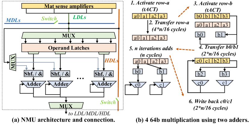
FHEmem supports in-memory computations by connecting each mat to a near-mat unit (NMU) via the local data lines (LDLs). Each NMU consists of full adders, shifters, AND logic, and latches to compute FHE operations, shown in Figure 5(a). In addition to the mat sense amplifiers, NMU can also receive data from other NMUs via inter-NMU connection. The design of NMU differs from previous PIM-logic integration, DRISA [10], in three ways. First, NMU places all customized logic outside the mat, which is optimized for area efficiency. On the contrary, DRISA [10] integrates logic and latches with the mat sense amplifiers and bitlines, which may incur significant changes to the area-optimized mat. Second, DRISA [10] integrates logic to all bitlines in a mat, causing a large area overhead while only gaining moderate performance benefits due to the unbalanced compute and data movement [10]. In FHEmem, we explore the processing throughput of NMU under different architecture configurations and observe the most efficient design does not adopt the maximum throughput (Section V). Third, NMU in FHEmem can support permutations required by FHE using multiplexers in the data path.
To compute FHE arithmetic (i.e., modular arithmetic), NMU requires several steps in mat, data links, and NMU. Figure 5(b) shows an example of processing 4 64b multiplications in an NMU with 2 64b adders. For generality, we denote each mat row can store N n-bit values (N=4 and n=64 in this example), and NMU has M n-bit adders. First, the mat must activate an operand row (1) and transfer the row to the row-size operand latches (2). Next, the mat activates the second operand row (3) and transfers M-value blocks to the shifter and AND logic (4). When both operands are ready, the shifter and AND logic will generate a partial product using the second operand (b0 and b1) and bit masks of a specific bit of the first operand (a0 and a1 in the latches). NMU takes n cycles to compute an n-bit multiplication (5). After processing an M-value block, NMU writes the result back to the mat (6) and loads the next M-value block for processing (7). Like DRISA [10], NMU only needs two row activations for each vector processing but requires serial data transfers via LDLs. NMU can serially write back values in a different order to support permutation.
III-B Inter-NMU Connection
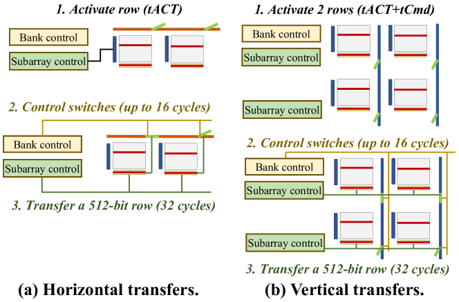
To efficiently process various FHE data transfer patterns, FHEmem enables data transfer between NMUs in horizontal and vertical directions. In the vertical direction, FHEmem utilizes the master data lines (MDLs) which connect all NMUs in the same mat column. In the horizontal direction, FHEmem adds extra data links, horizontal data links (HDLs), to each subarray (a row of mat). The HDLs in each subarray support the same bitwidth as the MDLs in each mat column (i.e., 16-bit). For both directional links, we add small isolation transistors (switch in Figure 5) [29] to serve as switches that can disconnect each link at a certain point. NMUs separated by the off switches can transfer data independently, significantly improving the bandwidth for intra-bank and intra-subarray data movements.
In FHEmem, each horizontal and vertical inter-NMU connection transfers a 512-bit mat row to another mat, where Figure 6 shows the detailed steps. Before transferring, FHEmem activates the participating row(s) in subarray(s). The horizontal (vertical) transfer requires the activation in 1 (2) subarray(s). FHEmem then turns on or off the switches based on the transfer pattern (Section III-D). To reduce the area and energy cost, FHEmem uses a single control signal for all switches in a row for vertical links (MDLs), similar to LISA [29]; for horizontal links (HDLs), FHEmem adopts a single control signal for all switches in a column. The bank-level logic has the bookkeeping logic for switches’ states. Setting up switches requires up to 16 cycles because we map each polynomial to a mat array (Section IV-A). Last, the subarray controller controls the near-mat peripheral to send/receive data based on the transfer pattern. Transferring 512-bit data via 16-bit data links requires 32 cycles.
III-C Inter-bank Connection
As introduced in Section II-A, FHE has dependencies between RNS polynomials of a ciphertext during BConv. To store a ciphertext, which can consist of tens of RNS polynomials, we need to distribute these RNS polynomials over multiple banks, and each BConv requires a large amount of inter-bank data transfers because of an all-to-all dependency. For such inter-bank data movements, a naive way is to use the conventional channel-level data bus. Unfortunately, such centralized data movements fail to match the throughput of in-memory computations, significantly slowing down the acceleration. Furthermore, the cost of fully-connected interconnect can be prohibitively high. To support the inter-bank communication with satisfactory performance, while introducing reasonable overhead in HBM, we propose a partial chain interconnect network between banks inside a channel. The partial chain network connects neighboring banks in each bank group, using 256b-wide transfer links and per-bank transfer buffers. Specifically, the transfer buffer in each bank can communicate with the local master data lines (MDLs) and the transfer links to the neighboring banks. We add two 256b transfer buffers in each bank to support seamless transfers between banks. The customized links and buffers enable parallel inter-bank data transfers across different banks in a channel, avoiding sequential transfers via the original channel IO. When transferring a whole row between two neighboring banks, the source bank drives 256b data blocks from the selected subarray SA via MDLs to the transfer buffer, which sends data blocks to the transfer buffer of the destination bank via either the customized links (neighboring banks) or the original channel IO (non-neighboring banks). The destination bank writes data blocks to the selected subarray SA via MDLs.
III-D FHEmem Controllers
| Command | Description | Cycles |
|---|---|---|
| nmu_ld | load data from SA column address to NMU latches | |
| nmu_st | store from NMU latch to SA column address | |
| nmu_hmov | horizontal data movement between NMUs in a subarray | |
| nmu_vmov | vertical data movement between subarrays | |
| nmu_add | Start addition using selected latches with or without shift &AND | |
| nmu_pst | store different NMU latches (64-bit) to SA column address | 4 |
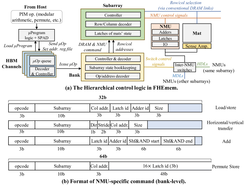
FHEmem needs modifications in bank/subarray controllers to support its various functions. To support the in-memory computation, FHEmem exploits the existing control logic of SIMDRAM [14]. Figure 7(a) shows the processing flow of hierarchical control with the annotation of FHEmem extension. The host CPU sends bbop instructions to each memory controller (i.e., channel-level controller in HBM). FHEmem requires an extension of bbop instructions for modular arithmetic and permutation for FHE. Each memory controller has a micro-program control logic that translates each bbop to a micro-program which is a sequence of DRAM subarray-level commands. Previous works [14] has shown the micro-program control logic only incurs negligible area overhead (less than ).
FHEmem extends the bank-level control to decode NMU commands and dispatches signals to subarray-level logic and the isolation transistors (switches). FHEmem requires the extra logic for subarray-level parallelism [27], including the bookkeeping logic in the bank controller for the status of all subarrays and the extra address latches in each subarray row decoder. The subarray-level control sends signals to all NMUs in the subarray based on the command. Furthermore, FHEmem adds more latches in the subarray column decoder to support the permutation operations. The extra logic and control signals in FHEmem also introduce insignificant overhead (Table III) because they are placed outside the mat.
FHEmem adds several new subarray-level commands for NMU processing, as shown in Table I and Figure 7(b). The subarray-level commands control the same behaviors of all mats/NMUs in a subarray, except which stores different latches in different mats back to SA (used for automorphism). For NMU loading and storing, FHEmem supports the flexibility of selecting columns in NMU latches, adder latches, and sense amplifiers, enabling permutation. The horizontal data movement has predefined patterns, defined by and , to support NTT data movements. The vertical data movement has more flexibility to transfer data between two subarrays. The command in FHEmem indicates the latch-adder pair for computation and whether to use shift/AND and the bit position of shift/AND. To exploit subarray-level parallelism and minimize the command patching latency (i.e., minimize the number of commands), most FHEmem commands, except the permute store (), can be configured for processing large data size.
Figure 7(b) shows the format of the 7 FHEmem commands (3-bit opcode). To support the precision requirement of FHE, each FHEmem command processes 64-bit data. Therefore, the column/latch address and the size of data of near-mat processing can be presented by 3 bits (i.e., 8 possible 64-bit data in 512-bit row in a mat). In our architectural exploration (Section V), each bank has 128 (ARx1) to 1024 (ARx8) subarrays, requiring 10-bit to denote the subarray. Each subarray contains 16 mats so we can use 3-bit mat id, 1-bit direction and 2-bit stride, to represent all horizontal movements in a subarray. The addition command includes a range of for multiplication - both the start and end shift steps can be represented by 6-bit (i.e., up to 64 bits). For the permute store command, a 48-bit field is reserved for the vector of latch addresses in 16 NMUs of a subarray. The issue time of 32-bit (64-bit) command to each bank via 16-bit command/address bus is 2 (4) cycles, respectively.
III-E Practicality of FHEmem
Commodity DRAMs are optimized for cost so that DRAM process only adopts 3 metal layers, with 1 layer (M1) for bitlines (vertical), 1 layer (M2) for LDLs and master word lines (MWLs) (horizontal), and 1 layer (M3) for column select lines (CSLs) and MDLs [30]. M1 layer is the only fine-pitch (low energy efficiency) layer, optimized for the area of bitlines in a mat. M2 and M3 support more energy-efficient wires with larger area overhead (i.e., 4x pitch of M1). The design of FHEmem considers the cost-efficiency of modifying commodity DRAM, avoiding the high-cost changes in cost-sensitive components. In FHEmem, the additional horizontal data lines are placed in M2 which incurs less pressure in the routing. M3 (vertical) is more dense than M2 (horizontal) because both CSLs and MDLs on M3 extend across multiple mats while M2 only has MWLs shared by multiple mats. Furthermore, HDLs connect NMUs, which are placed outside of dense mats (DRAM cell arrays). As illustrated in previous work [30], changes near the mat are the most costly, including bitline sense amplifiers, local wordline drivers, row logic, and column logic. Changes outside the subarray logic are relatively inexpensive because of the low-density logic blocks. These characteristics make HDLs and NMUs more practical than previous PIM solution that integrates complex logic in bitline sense amplifiers (e.g., DRISA [10]) in conventional DRAM technology.
IV Optimized Processing Flow of FHE in FHEmem
The proposed FHEmem hardware supports high-throughput computations and data movements. The next challenge is to efficiently utilize FHEmem for FHE applications. This section introduces an optimized end-to-end processing flow that determines the data layout and processing flow of FHEmem for FHE applications by adopting several algorithm and compiler-level optimizations.
IV-A FHEmem Data Layout
In PIM acceleration, data layout is critical to determine the detailed computation and data movement. Figure 8 shows the optimized data layout in FHEmem. Each ciphertext contains a group of RNS polynomials, each of which is a vector of -bit integers. To exploit the high throughput of PIM, we distribute RNS polynomials of a ciphertext, including the original RNS terms () and the special terms () used for key switching, across multiple banks using a round-robin method. The figure shows an example of allocating two original RNS terms and two special RNS terms in a bank.
IV-A1 Layout in subarray groups
We divide subarrays into subarray groups, basic memory partitions for polynomials. Specifically, each subarray group contains a continuous set of subarrays (e.g., 2 subarrays) which is a 2D array of mats (e.g., 22). The 2D distribution allows FHEmem to balance the inter-mat data movements during various FHE operations (esp. NTT). FHEmem distributes coefficients of a polynomial across the mat array in an interleaved way, similar to previous work [5], to efficiently support automorphism (Section IV-E). In our setting, each subarray group contains 16 subarrays (16 16 mats), requiring each mat to use 32 rows to store 256 64-bit coefficients.
IV-A2 Layout for computation
For a computation using two RNS polynomials, we align both polynomials in the same column in a subarray. Each subarray group reserves rows for operand polynomials used for computation, including key-switching keys, constant polynomials, and other ciphertexts. If a subarray group computes with two polynomials in different subarray groups, the memory issues data movements that may happen inside a bank or across different banks.
IV-A3 Layout for constants
In addition to RNS polynomial, we need to allocate rows for several constants for FHE operations, including (i)NTT twiddle factors, moduli, scaled inverse moduli, etc. To avoid duplicating twiddle factors across NTT steps that require large memory, we store the vector of twiddle factors which contains -th roots of unity, in the same order as the polynomial coefficients. Before each (i)NTT stage , FHEmem first dynamically computes the twiddle factor for coefficient by multiplying the twiddle factor in the previous stage with . For moduli, we keep one copy in each mat in the subarray group, so that each NMU can load the corresponding value independently during the computation.
IV-B Algorithm-optimized modular reduction
A modular reduction follows each FHE arithmetic. We exploit the Montgomery algorithm [31] requiring two multiplications, one addition, and one subtraction. NMUs in FHEmem processes n-bit multiplication using n serial additions. Therefore, we exploit algorithm optimization to significantly reduce the latency and energy for modular arithmetic. Specifically, we select moduli that are friendly to serial computations while satisfying security requirements and (i)NTT. We exploit the moduli selection technique proposed in previous works [32] that select moduli has the form of , where is called hamming weight. Using a modulus with a hamming weight of , we only need to issue additions during the multiplication, hence reducing the addition steps from to . The hamming weight optimization only applies to computations with constant, including the multiplication with modulus and the multiplication with reduction factor in Montgomery reduction. The advantage of Montgomery reduction over Barrett reduction [33] is that both reduction factor and modulus in Montgomery reduction can have a low hamming weight, and it only requires single bit-length computation. We note that prior FHE accelerators [6] also adopted a similar optimization that customized the modular multiplier for Montgomery-friendly moduli. However, their modular multipliers cannot process computations using moduli with different characteristics (e.g., required by other applications). FHEmem provides more flexibility by using addition as the basic computing step.
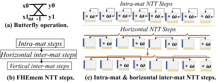
IV-C FHEmem NTT
NTT executes several steps of permutation and computations. Each NTT step requires several butterfly operations (Figure 9(a)) on pairs of coefficients, that multiply the coefficients with the twiddle factors, permute the coefficients, and then update the coefficients. FHEmem processes each (i)NTT operation in three stages, intra-mat, horizontal inter-mat, and vertical inter-mat, depending on the butterfly stride of each (i)NTT step (Figure 9(b)). For intra-mat steps, where coefficients of each butterfly operation are in the same mat, NMUs in a subarray group independently process computation and permutation. The horizontal inter-mat steps exchange the coefficients between mats in the same row, for which FHEmem uses HDLs for efficient data transfers, as shown in Figure 9(c). Specifically, FHEmem turns on/off the switches of NMUs on HDLs, where the connected segments can independently transfer data. Data transfers using the same connected segment are scheduled sequentially. Therefore, as the number of connected segments changes over (i)NTT stages, the transfer latency of different (i)NTT stages varies. The vertical inter-mat NTT steps are processed similarly to the horizontal steps but using MDLs. The key novelty of FHEmem on (i)NTT operations is that FHEmem does not introduce complex butterfly networks in the memory. Instead, FHEmem exploits the existing DRAM internal links (i.e., MDLs and LDLs) with efficient customizations (i.e., NMU, switches, HDLs).
IV-D Base Conversion
BConv is a costly but frequent operation in FHE. As introduced in Section II, to generate each special RNS polynomial of BConv (with modulus ), each input RNS polynomial with modulus first multiplies and . Such partial products are reduced to each special RNS polynomial . FHEmem parallelizes multiplications in different subarray groups with different input polynomials. To reduce the partial products, FHEmem first accumulates partial products in the same bank using NMUs and MDLs because partial products of different polynomials in a bank are aligned either in the same subarray group or in different subarray groups in the vertical direction. Therefore, the intra-bank accumulation can be processed in an adder-tree manner by exploiting switches in MDLs. FHEmem processes the final reduction in the bank of the output polynomial, requiring data transfers of partial products from all other banks. FHEmem handles such inter-bank data movements using the customized interconnection (Section III-C). To parallelize the computation, each bank processes different output polynomials simultaneously. FHEmem determines the optimized schedule based on the number of banks used for the ciphertext, the number of input/output RNS polynomials, and the underlying interconnect structure.
IV-E Automorphism
Automorphism is a process that permutes the coefficients of a polynomial by using Galois group. FHEmem supports automorphism based on the observation from BTS [5]: the interleaved coefficients (Section IV-A) in the same tile (mat in FHEmem) will be mapped to a single tile after automorphism. FHEmem further extends this idea to interleave coefficients in one more dimension, memory row, where the column of row of a mat stores coefficients with the indices . With such coefficient mapping, the automorphism only requires three steps: permutations in each row, vertical inter-mat permutation, and horizontal inter-mat permutation. FHEmem can handle the first step in NMU and the last two steps using MDLs and HDLs respectively.
IV-F Application Mapping Framework for FHEmem
FHEmem can provide large throughput when fully utilizing memory. However, it is not trivial to map a full FHE program to FHEmem hardware with high utilization. Thus, we propose a mapping framework that generates data layout and scheduling in a pipeline manner that can fully utilize the memory to process multiple input data in parallel.
IV-F1 Framework Overview
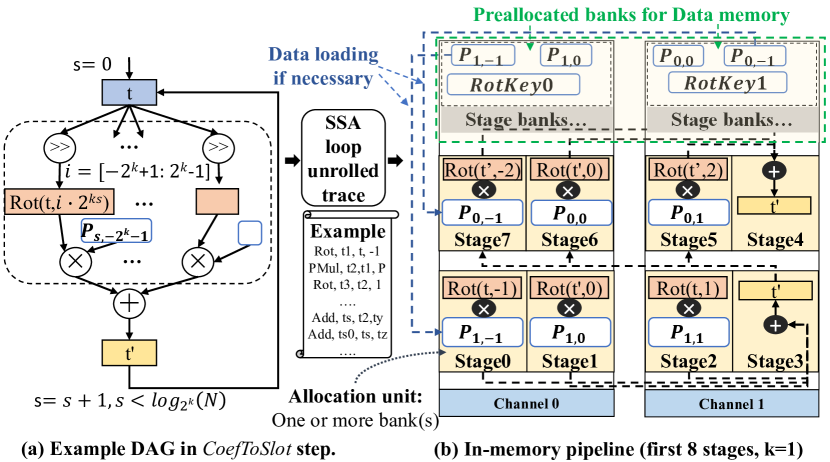
Figure 10 shows an example pipeline for the CoefToSlot step in CKKS bootstrapping. The input of our framework is an intermediate representation extracted from the real FHE program. Our framework generates a trace of FHE operations (e.g., HMul, HAdd, and HRot) in the static single-assignment (SSA) form while unrolling all loops. Our framework then divides the operation trace into multiple pipeline stages. The example shows the first 8 pipeline stages for CoefToSlot in a simplified HBM model with 2 channels. After computation on a stage, the allocated memory needs to transfer data to the memory that processes the pipeline steps with a data dependency. Therefore, the latency of each pipeline stage includes loading time, computation time, and transfer time. Our framework aims to minimize the latency of the bottleneck stage in the pipeline.
IV-F2 Memory Allocation for Pipeline Stages
Our framework allocates each stage to a basic allocation memory unit, whose size is determined by the FHE parameter setting including the polynomial degree, ciphertext scaling factor, and ciphertext moduli. In Figure 10, the basic memory unit is one bank. To process a stage, we need sufficient memory to support the data layout shown in Section IV-A for the input and output data. Extra memory is needed for constant data (e.g., evk and plaintexts). The ideal case is each allocation unit can hold all data for the stage. When a memory allocation unit cannot hold all data, we store constant data in a reserved memory location called data memory. When data is stored in the data memory, all operations (across all stages) requiring the data need to dynamically load it. We reduce the memory footprint by storing data in one place, instead of duplicating them in different memory locations.
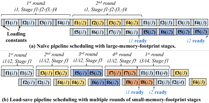
IV-F3 Load-save Pipeline
A naive way of pipeline generation is to divide the FHE program into stages, where is the number of available allocation units in memory. However, for large applications, each stage may require a large memory footprint for operations, leading to frequent constant loading. As shown in Figure 11(a), a stage has 4 operations, and every operation needs to load constants because memory is occupied by the constants of previous operations. In FHEmem, we propose a load-save pipeline by dividing operations into fine-grained stages with a small enough footprint. The fine-grained stages are allocated to different memory in a round-robin manner, requiring multiple rounds to process all stages for an input. In each round, the memory only creates a pipeline with part of the program (f1 and f2 in the first round in Figure 11(b)). It runs through a batch of input with only 1 data loading at the beginning of each round. Each memory loads the next round of stages when the current input batch is completed. The load-save pipeline minimizes the data loading while still fully utilizing the memory for computation.
V Experimental Setup
| HBM configuration | 8-high HBM2E (16GB/stack)@10nm |
|---|---|
| Memory organization | #banks/pseudo-channel=8, #pseudo-channels/stack=32 |
| Bank specification | 64MB, row_size=1kB, 512*512 mats |
| Data transfer | inter-bank NoC = 256-bit |
| Timing (ARx1) | , , , |
| Energy @10nm (ARx1) | , |
| , |
V-A Hardware Evaluation
Memory Technology: The basic architecture of FHEmem is similar to HBM2E [34, 35]. The system configuration is shown in Table II. Each HBM2E stack has 16GB with 16 physical channels. We scale energy and power values from 22nm used in previous work [36] to 10nm (shown in Table II), based on the recent HBM2E technology [34]. We follow the method of Vogelsang [30] to calculate the scaling factors for energy. We assume 16 physical channels on a stack are connected by a crossbar on PHY where each bidirectional link is 64-bit wide (bisection bandwidth=64GB/s per stack). We also add stack-stack links for scaled-up systems, commonly used in memory-centric architecture [37]. FHEmem has two HBM2E stacks to support 32GB memory. We exploit the remaining signaling links on HBM2E for stack-stack connection so the inter-stack bandwidth is also 256GB/s.
Hardware Modeling: To evaluate the area and power of customized components, we synthesize our design in 45nm technology using Nangate Open Cell Library. We model all other CMOS components (including buffers and interconnects) in Cacti [38] at 32nm technology. We scale all values to the 10nm technology with the scaling factors calculated from previous work [39]. We estimate the delay, power, and area overhead of integrating CMOS-ASIC and DRAM technologies based on the difference in number of metal layers and complexity of the customized logic [10].
Simulation: We generate FHE operation traces from software implementations of different workloads, and our mapping framework optimizes the trace and generates PIM instructions for simulation. Our in-house simulator adopts a cycle-accurate trace simulation based on the standardized DRAM latency constraints, similar to Ramulator [40]. We model control logic at different levels in the DRAM hierarchy.
V-B Workloads
Logistic Regression (HELR) [19]: This workload has 30 iterations of homomorphic logistic regression where each iteration trains 1024 samples with 256 features as a batch. The multiplication depth is deep, requiring several bootstrappings.
ResNet-20 [20]: The ResNet-20 is a homomorphic neural network inference for one CIFAR-10 image classification. The network is deep with multi-channel convolutions, matrix multiplications, and approximated ReLU function.
Sorting [41]: Sorting uses 2-way bitonic sorting on an array with 16,384 elements, the same as that used in SHARP [8].
V-C FHE Parameters and Evaluation
We evaluate the efficiency of FHEmem on a 128-bit security FHE parameter setting chosen from Lattigo [42]. For workloads with bootstrapping, including HELR, ResNet-20, and sorting, we use , , , and , similar to prior accelerators [5, 7]. Each polynomial is decomposed into 40-61 bit RNS terms, where FHEmem allocates 64-bit for each coefficient. For shallow LOLA workloads, we use the similar parameter settings with CraterLake [6], where we assume , , and . FHEmem represents 32-bit coefficients in 64-bit words and packs 4 RNS polynomials together in 16 subarrays. For all workloads, we measure the maximum time across all pipeline stages, indicating the time we can finish an input when the pipeline is full. In addition, we consider the number of pipelines that can be processed simultaneously in the system when the program cannot fully utilize the memory capacity (e.g., 32GB).
VI Evaluation
VI-A Comparison to Previous FHE Accelerators
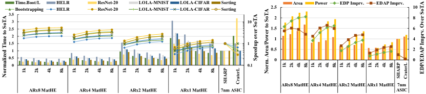
Figire 12 compares FHEmem with two state-of-the-art ASIC FHE accelerators (CraterLake [6], and SHARP [8]). We explore two design choices of memory organization that play important roles in the performance, power, and area of FHEmem: the aspect ratio of DRAM mat (AR), and the width of adders in a subarray (if each NMU has 2 64-bit adders, a subarray with 16 mats has 2k-width adders). As discussed in Section II-D, high-AR architecture has better performance and energy efficiency than low-AR architecture, but incurs significant area overhead. The width of adders determines the performance of arithmetic computing - wide adder designs support faster computing while requiring a larger area than narrow adders. For the chip area of prior ASIC accelerators, we add the area of 32GB HBM2E (2110) for a fair comparison.
VI-A1 Performance
FHEmem shows superior performance over prior FHE accelerators. Specifically, ARx8-8k (lowest EDP) is 4.4 (8.8), 2.2 (3.4), and 5.4 (17.5) faster than SHARP [8] (CraterLake [6]) on bootstrapping, HELR, and ResNet-20 respectively. ARx4-4k (lowest EDAP) is 3.4 (6.8), 1.7 (2.6), and 4.1 (13.2) faster than SHARP [8] (CraterLake [6]) on bootstrapping, HELR, and ResNet-20 respectively. For sorting, ARx8-8k (ARx4-4k) is 4.2 (3.1) faster than SHARP [8]. For LOLA-MNIST and LOLA-CIFAR, ARx8-8k (ARx4-4k) are 3.0 (2.1) and 3.2 (2.3) faster than CraterLake [6]. The less significant performance improvement in HELR results from the low portion of bootstrapping which is significantly optimized by adopting the minimum-key optimization [7, 8].
VI-A2 Efficiency
We then compare the power and area efficiency of FHEmem and ASIC accelerators. Compared to SHARP, ARx8-8k improves EDP and EDAP by 8.2 and 5.1. However, ARx8-8k requires 1.6 larger area and 2.3 higher power than SHARP. ARx4-4k improves EDP and EDAP of SHARP [8] by 6.2 and 6.9, with 0.9 area and 1.8 power consumption. ARx2-2k is a configuration that provides the best performance using less area (0.65) and power (0.94) than SHARP. For performance, ARx2-2k is 1.56, 0.92, and 1.96 faster than SHARP, leading to 2.59 and 3.96 EDP and EDAP improvement.
VI-A3 Analysis of FHEmem Benefits
Compared to ASIC accelerators, FHEmem provides a higher throughput due to the efficient in-memory computation and large intra-memory bandwidth. For instance, ARx4-4k FHEmem has 16 million 64-bit adders. Considering the cost of DRAM row activations, data transfers, subarray-level parallelism, and 500MHz frequency of additions, the effective throughput of ARx4-4k for 64-bit multiplication is around 637.61 TB/s. During multiplication, the adders consume most of the energy because row activation energy is amortized for the entire row, and data transfer is energy-efficient due to the short wire length. Therefore, the energy efficiency of FHEmem computation is similar to the modular multiplier used by FHE accelerators (slightly higher due to the DRAM-CMOS integration). For the internal bandwidth of NTT, ARx4 FHEmem supports a 256-bit link (500MHz) for each of the 512 subarrays in a bank. Considering up to half of the subarrays can transfer data simultaneously during NTT, the peak internal bandwidth for NTT is 2048 TB/s in 32GB ARx4 FHEmem. For the slowest NTT step, the internal bandwidth drops by 16 (128 TB/s). As a comparison, SHARP [8] has around 24K 36-bit multipliers running at 1GHz, leading to 221.18 TB/s throughput. Furthermore, the on-chip memory resources in SHARP support 72TB/s bandwidth.
VI-B Comparison across different FHEmem Configurations
As shown in Figure 12, There is a significant difference in power and area between different FHEmem configurations. For example, the most oversized FHEmem (ARx8-8k) requires 642.32 chip area and 218W power, while the smallest FHEmem (ARx1-1k) only requires 223.81 chip area and 36.24W power. As a reference, the commercial 2-stack HBM2E has a chip area of 220 [34] and the power budget of a conventional HBM system is 60W [36]. We note that the power budget of conventional HBM is different from the accelerator design targeted in this work, where high power consumption is reasonable if it meets the thermal requirement (e.g., 10W//layer [43]).
Based on the results, high-AR FHEmem provides higher performance than low-AR designs because increasing AR can increase both compute and data movement throughput inside a bank. For ARx1 and ARx2 FHEmem configurations, doubling AR can provide 1.57 to 1.98 speedup because the execution is compute-bound. For ARx4, doubling AR only provides 1.23 to 1.67 speedup. Increasing adder-width exhibits a similar trend where the effect of increasing compute resources diminishes for high-throughput architectures.
To find the most cost-efficient FHEmem design, we evaluate energy-delay-product (EDP) and energy-delay-area-product (EDAP) for different FHEmem configurations. For EDP, the trend follows the performance, where the largest FHEmem (ARx8-8k) gives the lowest EDP. When considering the area cost, different ARs favor different adder widths. Specifically, ARx8 and ARx4 exhibit the lowest EDAP at 2k and 4k adder-width respectively. The configuration with the lowest EDAP (ARx4-4k) is 1.34 more efficient than ARx8-8k.
VI-C FHEmem Latency and Energy Analysis
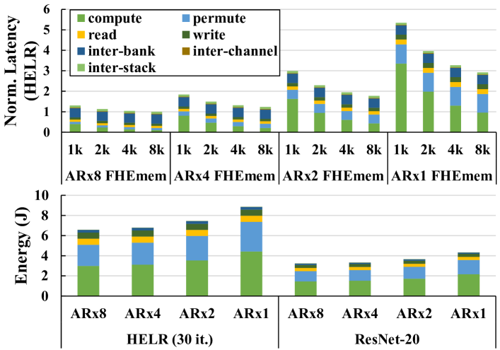
Figure 13 shows the latency and energy breakdown of different FHEmem configurations. Considering the parallel processing, we accumulate all latency values across all memory banks for the latency breakdown. We divide all operations into 7 categories, including computation (subarray activation/precharge, operand transfer, and addition), permutation (inter-mat transfer), read/write (activation and precharge for data transfers), and inter-bank/channel/stack IO traffics.
The breakdown results provide several key insights into FHEmem. First, in low-AR FHEmem, the latency is dominated by computation and permutation because of the limited throughput of computation and intra-bank data movements. Increasing AR can effectively reduce the latency for both computation and permutation latency. Furthermore, increasing the adder width can effectively reduce the computation latency. However, in high-AR FHEmem, the data movement becomes the performance-dominant operation, especially inter-bank data movements (mainly caused by BConv). This proves the necessity of customized inter-bank links. We analyze the detailed effect of optimizations in Section VI-F. For energy consumption, FHEmem consumes most of the energy on computation and permutation, which incurs intensive row-activation and intra-bank data movements.
VI-D PIM Technologies
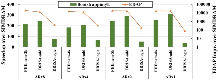
Figure 14 compares the efficiency of FHEmem to other PIM technologies, including SIMDRAM [14] and DRISA [10]. For a fair comparison, we use the proposed application mapping and customized data links in baseline PIM architectures, while evaluating the difference in processing. We implement an adder-less NMU for permutations in baselines. We select the most efficient (lowest EDPA) FHEmem for each AR. The results show FHEmem is 183.7 to 255.4 faster than SIMDRAM [14], and 2.76 to 6.75 faster than DRISA-logic [10]. Furthermore, FHEmem is at least 19,300 and 47 more efficient than SIMDRAM and DRISA-logic using EDAP. Compared to DRISA-add [10], FHEmem is 1.14 to 1.21 slower from ARx8 to ARx1 because DRISA’s adders can directly access the sense amplifiers. However, FHEmem is 1.04 (ARx1) to 1.51 (ARx8) more efficient in EDAP because FHEmem does not introduce area overhead in a mat. Furthermore, DRISA is more challenging to manufacture because the large adder area will affect the alignment of cost-optimized bitlines. As a comparison, FHEmem puts all customized logic outside the mat structure.
VI-E Overhead Analysis
| ARx4 HBM | DRAM Cell | Local WL Driver | Sense Amp | Row/Col Dec.s |
|---|---|---|---|---|
| Area () | 56.54 | 26.15 | 45.63 | 0.39 |
| Center Bus | Data Bus | TSV | Total | |
| 1.56 | 4.81 | 13.25 | 148.33 | |
| 4K adder | Horizontal DL | Adder&Latches | Bank Chain & Buf. | Control logic |
| Area () | 14.13 | 30.43 | 0.065 | 0.56 |
| Power/Energy | 5.3fJ/b (avg.) | 15.86W | 0.53pJ/b | 0.12W |
Table III shows the area and power breakdown for our customized hardware components of FHEmem based on 1 HBM2E stack (16GB). We exploit the Cacti-7 [38] to generate the area breakdown of HBM and rescale the values to the published work [34]. The table shows a structure of ARx4 HBM and each subarray contains 4k-wide adders. All area values are for a single layer. The large area mainly comes from the near-mat adders. The horizontal data links use the same technology as the global data lines with the consideration of energy efficiency ( larger than local bit-lines). We extract the capacitance of material and scaling method from previous work [30] to calculate the energy consumed by data transfer. We note that the target of FHEmem is not a cost-optimized memory product, but a specialized accelerator for emerging applications that require high-throughput computation and/or efficient intra-memory data movements. However, the proposed design is still practical regarding area and power overhead. First, unlike previous near-subarray PIM [10], FHEmem put the customized logic outside DRAM mat, avoiding the issue of aligning cost-efficient local bitlines. Second, FHEmem can maintain an average DRAM working temperature (under 85). Previous work [43] shows a 16-high compute-centric 3D memory can tolerate 10W/ per memory layer to keep DRAM temperature under the 85 limit with a commodity-server active heat sink. For example, the power consumption and area of 8-high ARx4 4k FHEmem are 173.9W and 367, resulting in a power density of 5.92W/ (the highest power density in our exploration).
VI-F Evaluation of FHEmem Optimizations
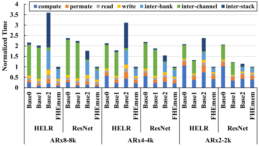
We compare FHEmem with baseline systems enabling a subset of FHEmem optimizations, as shown in Figure 15.
VI-F1 Montgomery-friendly Moduli
The Montgomery-friendly moduli can reduce the number of addition steps, improving the computation performance. As shown in Figure 15, Base1 is 1.68 and 1.58 faster than Base0 on HELR and ResNet with ARx2-2k architecture. On Arx4 and Arx8 architectures, this optimization only improves the performance by 1.17 and 1.06. However, Montgomery-friendly moduli can reduce energy consumption by 1.75 because computation is energy-dominant across all FHEmem architectures (Figure 13).
VI-F2 Interconnect Network
The comparison between FHEmem and Base1 shows the efficiency of the proposed inter-bank network, where Base1 uses the existing HBM channel IO for all inter-bank data movements. Based on our results, the proposed inter-bank network can improve the performance by 1.31, 1.86, and 2.12 on ARx2, ARx4, and ARx8 respectively. The inter-bank network can reduce the latency of related data movement by 3.2 on average.
VI-F3 Load-save Pipeline Mapping
The comparison between FHEmem and Base2 shows the efficiency of the load-save pipeline mapping. For HELR, load-save pipeline mapping improves the performance by 3.59 (1.77), 3.12 (1.54), and 2.38 (1.15) on ARx8, ARx4, and ARx2, respectively, for HELR (ResNet). The significant performance improvement results from reducing frequent data loading, especially data from a remote stack.
VII Related Work
Several FHE-specific accelerators have been proposed recently in the architecture community [44, 6, 5, 7, 8]. HEAX [45] is an FPGA-based accelerator targeting the CKKS FHE scheme, and accelerates FHE primitives (e.g., multiplication and key-switching) by up to 200; HEAWS [46] is also an FPGA implementation on Amazon AWS FGPAs, which accelerates B/FV FHE scheme (5 on a microbench). CraterLake [6] adopts wide vector processor with specialized high-throughput units for BConv and on-chip key generation. BTS [5] exploits relatively low throughput function units with large inter-PE crossbar network. ARK [7] uses an algorithm-hardware co-design to significantly reduce the off-chip bandwidth for bootstrapping and plaintext polynomials. SHARP [8] further improves the performance ARK by using low bit-precision data path (36-bit vs. 64-bit in ARK). However, their technique does not apply to general and ciphertexts, leading to the same memory issues, as analyzed in Section II. FHEmem exploits the large internal memory bandwidth of memory-based acceleration to unleash the processing throughput in a more area and power-efficient way.
CryptoPIM [44] is a ReRAM-based PIM accelerator with customized interconnect for NTT operations, lacking the support for more general FHE operations. In-storage processing is another promising technology to accelerate big-data applications [47]. INSPIRE is an in-storage processing system for private database queries based on FHE by integrating FHE logic (e.g., NTT and permutation) in the SSD channels. INSPIRE only supports small FHE parameters (i.e., N=4096) and its throughput is limited by the number of SSD channels. MemFHE [9] is a ReRAM-based PIM accelerator with the customized data path for bit-level TFHE scheme, not applicable to CKKS and other packed FHE schemes.
VIII Conclusion
This work proposes FHEmem, an FHE accelerator based on a novel near-mat processing architecture with relatively lightweight hardware modifications in conventional HBM. We also propose the end-to-end processing flow with a mapping framework for PIM-based FHE. Our evaluation shows FHEmem is 6.9 more efficient than prior-art ASIC accelerator.
Acknowledgement
This work is supported by SRC HWS, SRC PRISM, and NSF fundings #2003279, #1911095, #1826967, #2100237, #2112167, #2052809, #2112665.
References
- [1] I. Chillotti, N. Gama, M. Georgieva, and M. Izabachène, “Tfhe: fast fully homomorphic encryption over the torus,” Journal of Cryptology, vol. 33, no. 1, pp. 34–91, 2020.
- [2] J. H. Cheon, A. Kim, M. Kim, and Y. Song, “Homomorphic encryption for arithmetic of approximate numbers,” in International Conference on the Theory and Application of Cryptology and Information Security. Springer, 2017, pp. 409–437.
- [3] C. Gentry, “Fully homomorphic encryption using ideal lattices,” in Proceedings of the forty-first annual ACM symposium on Theory of computing, 2009, pp. 169–178.
- [4] Z. Brakerski, C. Gentry, and V. Vaikuntanathan, “(leveled) fully homomorphic encryption without bootstrapping,” ACM Transactions on Computation Theory (TOCT), vol. 6, no. 3, pp. 1–36, 2014.
- [5] S. Kim, J. Kim, M. J. Kim, W. Jung, M. Rhu, J. Kim, and J. H. Ahn, “Bts: An accelerator for bootstrappable fully homomorphic encryption,” arXiv preprint arXiv:2112.15479, 2021.
- [6] N. Samardzic, A. Feldmann, A. Krastev, N. Manohar, N. Genise, S. Devadas, K. Eldefrawy, C. Peikert, and D. Sanchez, “Craterlake: A hardware accelerator for efficient unbounded computation on encrypted data,” in Proceedings of the 49th Annual International Symposium on Computer Architecture, ser. ISCA ’22. New York, NY, USA: Association for Computing Machinery, 2022, p. 173–187. [Online]. Available: https://doi.org/10.1145/3470496.3527393
- [7] J. Kim, G. Lee, S. Kim, G. Sohn, M. Rhu, J. Kim, and J. H. Ahn, “Ark: Fully homomorphic encryption accelerator with runtime data generation and inter-operation key reuse,” in 2022 55th IEEE/ACM International Symposium on Microarchitecture (MICRO), 2022, pp. 1237–1254.
- [8] J. Kim, S. Kim, J. Choi, J. Park, D. Kim, and J. H. Ahn, “Sharp: A short-word hierarchical accelerator for robust and practical fully homomorphic encryption,” in Proceedings of the 50th Annual International Symposium on Computer Architecture, ser. ISCA ’23. New York, NY, USA: Association for Computing Machinery, 2023. [Online]. Available: https://doi.org/10.1145/3579371.3589053
- [9] S. Gupta, R. Cammarota, and T. v. Rosing, “Memfhe: End-to-end computing with fully homomorphic encryption in memory,” ACM Trans. Embed. Comput. Syst., nov 2022, just Accepted. [Online]. Available: https://doi.org/10.1145/3569955
- [10] S. Li, D. Niu, K. T. Malladi, H. Zheng, B. Brennan, and Y. Xie, “Drisa: A dram-based reconfigurable in-situ accelerator,” in Annual IEEE/ACM International Symposium on Microarchitecture (MICRO), 2017, pp. 288–301.
- [11] M. Imani, S. Gupta, Y. Kim, and T. Rosing, “Floatpim: In-memory acceleration of deep neural network training with high precision,” in 2019 ACM/IEEE 46th Annual International Symposium on Computer Architecture (ISCA). IEEE, 2019, pp. 802–815.
- [12] C. Eckert, X. Wang, J. Wang, A. Subramaniyan, R. Iyer, D. Sylvester, D. Blaaauw, and R. Das, “Neural cache: Bit-serial in-cache acceleration of deep neural networks,” in 2018 ACM/IEEE 45th Annual International Symposium on Computer Architecture (ISCA). IEEE, 2018, pp. 383–396.
- [13] F. Gao, G. Tziantzioulis, and D. Wentzlaff, “Computedram: In-memory compute using off-the-shelf drams,” in Proceedings of the 52nd annual IEEE/ACM international symposium on microarchitecture, 2019, pp. 100–113.
- [14] N. Hajinazar, G. F. Oliveira, S. Gregorio, J. a. D. Ferreira, N. M. Ghiasi, M. Patel, M. Alser, S. Ghose, J. Gómez-Luna, and O. Mutlu, SIMDRAM: A Framework for Bit-Serial SIMD Processing Using DRAM. New York, NY, USA: Association for Computing Machinery, 2021, p. 329–345. [Online]. Available: https://doi.org/10.1145/3445814.3446749
- [15] M. Zhou, W. Xu, J. Kang, and T. Rosing, “Transpim: A memory-based acceleration via software-hardware co-design for transformer,” in 2022 IEEE International Symposium on High-Performance Computer Architecture (HPCA). IEEE, 2022, pp. 1071–1085.
- [16] S. Lee, S.-h. Kang, J. Lee, H. Kim, E. Lee, S. Seo, H. Yoon, S. Lee, K. Lim, H. Shin, J. Kim, O. Seongil, A. Iyer, D. Wang, K. Sohn, and N. S. Kim, “Hardware architecture and software stack for pim based on commercial dram technology : Industrial product,” in 2021 ACM/IEEE 48th Annual International Symposium on Computer Architecture (ISCA), 2021, pp. 43–56.
- [17] Y. Kwon, K. Vladimir, N. Kim, W. Shin, J. Won, M. Lee, H. Joo, H. Choi, G. Kim, B. An, J. Kim, J. Lee, I. Kim, J. Park, C. Park, Y. Song, B. Yang, H. Lee, S. Kim, D. Kwon, S. Lee, K. Kim, S. Oh, J. Park, G. Hong, D. Ka, K. Hwang, J. Park, K. Kang, J. Kim, J. Jeon, M. Lee, M. Shin, M. Shin, J. Cha, C. Jung, K. Chang, C. Jeong, E. Lim, I. Park, J. Chun, and S. Hynix, “System architecture and software stack for gddr6-aim,” in 2022 IEEE Hot Chips 34 Symposium (HCS), 2022, pp. 1–25.
- [18] J. Ahn, S. Hong, S. Yoo, O. Mutlu, and K. Choi, “A scalable processing-in-memory accelerator for parallel graph processing,” in Proceedings of the 42nd Annual International Symposium on Computer Architecture, 2015, pp. 105–117.
- [19] K. Han, S. Hong, J. H. Cheon, and D. Park, “Logistic regression on homomorphic encrypted data at scale,” in Proceedings of the AAAI Conference on Artificial Intelligence, vol. 33, no. 01, 2019, pp. 9466–9471.
- [20] J.-W. Lee, H. Kang, Y. Lee, W. Choi, J. Eom, M. Deryabin, E. Lee, J. Lee, D. Yoo, Y.-S. Kim, and J.-S. No, “Privacy-preserving machine learning with fully homomorphic encryption for deep neural network,” IEEE Access, vol. 10, pp. 30 039–30 054, 2022.
- [21] A. Brutzkus, R. Gilad-Bachrach, and O. Elisha, “Low latency privacy preserving inference,” in International Conference on Machine Learning. PMLR, 2019, pp. 812–821.
- [22] K. Han and D. Ki, “Better bootstrapping for approximate homomorphic encryption,” in Cryptographers’ Track at the RSA Conference. Springer, 2020, pp. 364–390.
- [23] C. Gentry, S. Halevi, and N. P. Smart, “Fully homomorphic encryption with polylog overhead,” in Annual International Conference on the Theory and Applications of Cryptographic Techniques. Springer, 2012, pp. 465–482.
- [24] J. H. Cheon, K. Han, A. Kim, M. Kim, and Y. Song, “A full rns variant of approximate homomorphic encryption,” in International Conference on Selected Areas in Cryptography. Springer, 2018, pp. 347–368.
- [25] N. Samardzic, A. Feldmann, A. Krastev, S. Devadas, R. Dreslinski, C. Peikert, and D. Sanchez, “F1: A fast and programmable accelerator for fully homomorphic encryption,” in MICRO-54: 54th Annual IEEE/ACM International Symposium on Microarchitecture, ser. MICRO ’21. New York, NY, USA: Association for Computing Machinery, 2021, p. 238–252. [Online]. Available: https://doi.org/10.1145/3466752.3480070
- [26] M.-J. Park, H. S. Cho, T.-S. Yun, S. Byeon, Y. J. Koo, S. Yoon, D. U. Lee, S. Choi, J. Park, J. Lee et al., “A 192-gb 12-high 896-gb/s hbm3 dram with a tsv auto-calibration scheme and machine-learning-based layout optimization,” in 2022 IEEE International Solid-State Circuits Conference (ISSCC), vol. 65. IEEE, 2022, pp. 444–446.
- [27] Y. Kim, V. Seshadri, D. Lee, J. Liu, and O. Mutlu, “A case for exploiting subarray-level parallelism (salp) in dram,” in 2012 39th Annual International Symposium on Computer Architecture (ISCA), 2012, pp. 368–379.
- [28] Y. H. Son, O. Seongil, Y. Ro, J. W. Lee, and J. H. Ahn, “Reducing memory access latency with asymmetric dram bank organizations,” SIGARCH Comput. Archit. News, vol. 41, no. 3, p. 380–391, jun 2013. [Online]. Available: https://doi.org/10.1145/2508148.2485955
- [29] K. K. Chang, P. J. Nair, D. Lee, S. Ghose, M. K. Qureshi, and O. Mutlu, “Low-cost inter-linked subarrays (lisa): Enabling fast inter-subarray data movement in dram,” in 2016 IEEE International Symposium on High Performance Computer Architecture (HPCA), 2016, pp. 568–580.
- [30] T. Vogelsang, “Understanding the energy consumption of dynamic random access memories,” in 2010 43rd Annual IEEE/ACM International Symposium on Microarchitecture. IEEE, 2010, pp. 363–374.
- [31] P. L. Montgomery, “Modular multiplication without trial division,” Mathematics of computation, vol. 44, no. 170, pp. 519–521, 1985.
- [32] S. Kim, K. Lee, W. Cho, Y. Nam, J. H. Cheon, and R. A. Rutenbar, “Hardware architecture of a number theoretic transform for a bootstrappable rns-based homomorphic encryption scheme,” in 2020 IEEE 28th Annual International Symposium on Field-Programmable Custom Computing Machines (FCCM), 2020, pp. 56–64.
- [33] P. Barrett, “Implementing the rivest shamir and adleman public key encryption algorithm on a standard digital signal processor,” in Proceedings on Advances in Cryptology—CRYPTO ’86. Berlin, Heidelberg: Springer-Verlag, 1987, p. 311–323.
- [34] C. Oh, K. C. Chun, Y. Byun, Y. Kim, S. Kim, Y. Ryu, J. Park, S. Kim, S. Cha, D. Shin, J. Lee, J. Son, B. Ho, S. Cho, B. Kil, S. Ahn, B. Lim, Y. Park, K. Lee, M. Lee, S. Baek, J. Noh, J. Lee, S. Lee, S. Kim, B. Lim, S. Choi, J. Kim, H. Choi, H. Kwon, J. J. Kong, K. Sohn, N. S. Kim, K. Park, and J. Lee, “22.1 a 1.1v 16gb 640gb/s hbm2e dram with a data-bus window-extension technique and a synergetic on-die ecc scheme,” in 2020 IEEE International Solid- State Circuits Conference - (ISSCC), 2020, pp. 330–332.
- [35] “JEDEC Standard JESD235: High Bandwidth Memory (HBM) DRAM,” JEDEC Solid State Technology Association, Virginia, USA, Standard, 2013.
- [36] M. O’Connor, N. Chatterjee, D. Lee, J. Wilson, A. Agrawal, S. W. Keckler, and W. J. Dally, “Fine-grained dram: Energy-efficient dram for extreme bandwidth systems,” in 2017 50th Annual IEEE/ACM International Symposium on Microarchitecture (MICRO). IEEE, 2017, pp. 41–54.
- [37] C. Giannoula, N. Vijaykumar, N. Papadopoulou, V. Karakostas, I. Fernandez, J. Gómez-Luna, L. Orosa, N. Koziris, G. Goumas, and O. Mutlu, “Syncron: Efficient synchronization support for near-data-processing architectures,” in 2021 IEEE International Symposium on High-Performance Computer Architecture (HPCA). IEEE, 2021, pp. 263–276.
- [38] N. Muralimanohar et al., “Optimizing nuca organizations and wiring alternatives for large caches with cacti 6.0,” in MICRO’07. ACM/IEEE, 2007.
- [39] A. Stillmaker, Z. Xiao, and B. Baas, “Toward more accurate scaling estimates of cmos circuits from 180 nm to 22 nm,” VLSI Computation Lab, ECE Department, University of California, Davis, Tech. Rep. ECE-VCL-2011-4, vol. 4, p. m8, 2011.
- [40] Y. Kim, W. Yang, and O. Mutlu, “Ramulator: A fast and extensible dram simulator,” IEEE Computer Architecture Letters, vol. 15, no. 1, pp. 45–49, 2016.
- [41] S. Hong, S. Kim, J. Choi, Y. Lee, and J. H. Cheon, “Efficient sorting of homomorphic encrypted data with k-way sorting network,” IEEE Transactions on Information Forensics and Security, vol. 16, pp. 4389–4404, 2021.
- [42] “Lattigo v4,” Online: https://github.com/tuneinsight/lattigo, Aug. 2022, ePFL-LDS, Tune Insight SA.
- [43] J.-H. Han, R. E. West, K. Torres-Castro, N. Swami, S. Khan, and M. Stan, “Power and thermal modeling of in-3d-memory computing,” in 2021 International Symposium on Devices, Circuits and Systems (ISDCS), 2021, pp. 1–4.
- [44] H. Nejatollahi, S. Gupta, M. Imani, T. S. Rosing, R. Cammarota, and N. Dutt, “Cryptopim: In-memory acceleration for lattice-based cryptographic hardware,” in 2020 57th ACM/IEEE Design Automation Conference (DAC), 2020, pp. 1–6.
- [45] M. S. Riazi, K. Laine, B. Pelton, and W. Dai, “Heax: An architecture for computing on encrypted data,” in Proceedings of the Twenty-Fifth International Conference on Architectural Support for Programming Languages and Operating Systems, 2020, pp. 1295–1309.
- [46] F. Turan, S. S. Roy, and I. Verbauwhede, “Heaws: An accelerator for homomorphic encryption on the amazon aws fpga,” IEEE Transactions on Computers, vol. 69, no. 8, pp. 1185–1196, 2020.
- [47] J. Lin, L. Liang, Z. Qu, I. Ahmad, L. Liu, F. Tu, T. Gupta, Y. Ding, and Y. Xie, “Inspire: In-storage private information retrieval via protocol and architecture co-design,” in Proceedings of the 49th Annual International Symposium on Computer Architecture, ser. ISCA ’22. New York, NY, USA: Association for Computing Machinery, 2022, p. 102–115. [Online]. Available: https://doi.org/10.1145/3470496.3527433