Electron correlation mediated site-selective charge compensation in polar/non-polar heterointerface
Abstract
One of the boundary conditions of the classical electromagnetic theory demands continuous electric potential across any boundary, which may not be naturally satisfied in atomically engineered heterostructures. Such polarity mismatch in oxide heterointerfaces is compensated through some (electronic/chemical/structural) reconstructions, leading to a myriad of emergent phenomena. The question we are posing is whether conventional semiconductor band bending framework is sufficient to comprehend compensation mechanisms in oxide heterostructures since, unlike semiconductors, complex oxides host strong electron correlations whose effects are indispensable. To address this, we investigate the interface between a prototypical insulating double perovskite Nd2NiMnO6 and a wide-bandgap insulator SrTiO3. This polar/non-polar interface offers a similar scenario as the famous LaAlO3/SrTiO3 system but with an exception - two transition metal sites with two individual correlated energy scales. By combining several experimental techniques and density functional theory, we establish a site-selective charge compensation process that occurs explicitly at the Mn site of the film, leaving the Ni sites inert. This surprising selectivity, which cannot be accounted by existing polar compensation mechanisms, is directly attributed to the TM cations’ relative correlation energy scales. This discovery presents that site-specific charge compensation can be a designer’s tool for tailoring emergent phenomena in oxide heterostructures.
Understanding the consequences of electrostatic boundary conditions at the interface between two dissimilar materials has been a long-standing and ever-explorative question in condensed matter physics [1]. Semiconductor heterostructures became a starting ground to study the effect of polarity mismatch, also termed as polar catastrophe, wherein Ge/GaAs heterostructure came to be studied in great detail since the 1970s [2]. Although both charge and atomic rearrangements were theoretically demonstrated as feasible ways to compensate the diverging potential [2, 3], no electronic reconstruction was observed experimentally [4, 5], which can be attributed to the lack of multiple valence states of elements present in a typical semiconductor heterostructure [6]. From this aspect, complex oxide heterostructures are fundamentally different as transition metal (TM) ions can easily access multiple valence states and have strong interplay amongst spin, charge, lattice, and orbital degrees of freedom [7, 8, 9]. In recent years, the impact of polarity mismatch in oxide heterostructures has become a research theme in itself, wherein a plethora of emergent phenomena such as two-dimensional electron gas [10, 11], superconductivity [12], ferromagnetism [13, 14, 15], superparamagnetism [16], etc. have been demonstrated. Unlike the case in a semiconductor, the potential divergence can be avoided here through either electronic/chemical reconstruction, resulting in a change in cationic valency [17, 18, 19, 20, 21, 22, 23] or structural effect such as interfacial intermixing [24, 25], intermediate layer formation [26], etc.
Another intricate factor inherent to TM oxides, specifically 3d TMOs, is that they are strongly correlated electron systems and are traditionally discussed by characteristic energy scales like the on-site coulomb repulsion energy (), charge transfer energy () and the hopping parameter () [27]. To examine whether these energies decide polar compensation process or a simple semiconductor-like band bending scenario is sufficient, we focus on the thin films of double perovskite (DP) oxide (A2BB’O6) [28] where B, B’ are the TM elements with their individual correlated energy scales. These materials themselves are interesting as they exhibit high-temperature ferromagnetism [29], room temperature magnetoresistance [30], multiglass behavior [31], insulating ferromagnetism [32, 33], etc. with lots of potential for technological applications.
In this work, we have investigated thin films of Nd2NiMnO6 (NNMO), grown on single crystalline NdGaO3 (NGO) (110)or [or represents orthorhombic coordinate system] and SrTiO3 (STO) (001) substrates by pulsed laser deposition (PLD) technique. Bulk NNMO is a monoclinic ferromagnetic insulator with a Curie temperature of 200 K [34]. Contrary to the NNMO film on NGO where both film and substrate consist of alternating +1 and -1 charged plane (hence no interfacial polarity mismatch), the NNMO/STO heterostructure encompasses interfacial polarity mismatch, similar to the well-known LaAlO3/SrTiO3 (LAO/STO) heterostructure [10]. We have explored the effect of polar catastrophe using element-sensitive X-ray absorption spectroscopy (XAS) and scanning transmission electron microscopy (STEM) measurements along with first principles calculations. Our findings establish that polar compensation happens through the formation of Mn3+ within the film side near the interface, while the Ni site remains unperturbed. The additional electron comes due to surface oxygen vacancies. This site-selective charge compensation emanates from the relative difference between and of Ni and Mn, demonstrating a direct connection between polarity compensation and electronic structure parameters in complex oxide heterostructures.
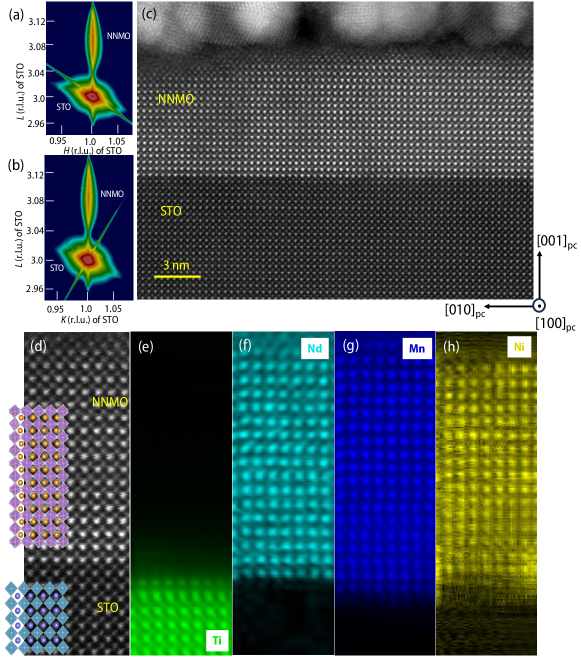
Sample fabrication and characterization: NNMO films of several film thicknesses [2, 3, 5, 10, and 20 uc, uc= unit cell in pseudocubic () notation] were grown on TiO2 terminated STO (001) substrates in layer-by-layer fashion using a PLD system, connected with a high-pressure reflection high energy electron diffraction (RHEED) setup. For comparison purposes, 5, 10, and 20 uc NNMO films were also grown on GaO2 terminated NGO (110)or [(001)pc] substrates. The epitaxial strain is calculated to be +0.4% and +1.5% for NNMO on NGO, and STO, respectively. The details of sample growth conditions and characterizations using RHEED, X-ray diffraction (XRD), and X-ray reflectivity (XRR) have been discussed in the Methods section. Fig. 1(a) and (b) show reciprocal space map (RSM) for the 20 uc NNMO film on STO in and plane around the (113)pc Bragg reflection of the substrate, recorded with synchrotron X-ray. The observation of the same and value for the film and substrate confirms that the film has the same in-plane lattice constants as the underlying STO. Using this RSM image, the out-of-plane lattice constant is found to be 3.803 Å, which is also very similar to the value found from a (00) crystal truncation rod measurement. RSM measurements for films grown on NGO also confirm the proper epitaxial relation between the film and substrate.
The epitaxial growth has been further confirmed by a cross-sectional scanning transmission electron microscopy (STEM) experiment on a 20 uc NNMO film on STO (experimental details are in the Methods section). As depicted in Fig. 1(c)-(d), high-angle annular dark field (HAADF) image along the zone axis [100] confirmed coherent epitaxial growth of the film on STO, devoid of any defect or dislocation. Atomically resolved electron energy loss spectroscopy (EELS) mapping [Fig. 1(e)-(h)] has found that the extent of cationic intermixing across the interface is limited to 1 uc on the film side, which is also consistent with the film/substrate interface roughness obtained from XRR fitting. Since such minuscule intermixing is very likely to be present in all films due to the use of same growth condition, it can not be the source of systematic changes in electronic structures with the film thickness, which are shown in the latter part of the paper. Another notable observation is that we do not find any NiO precipitation, which was reported to be the polar compensation mechanism for a thick ( 40 nm) La2NiMnO6 film [35].
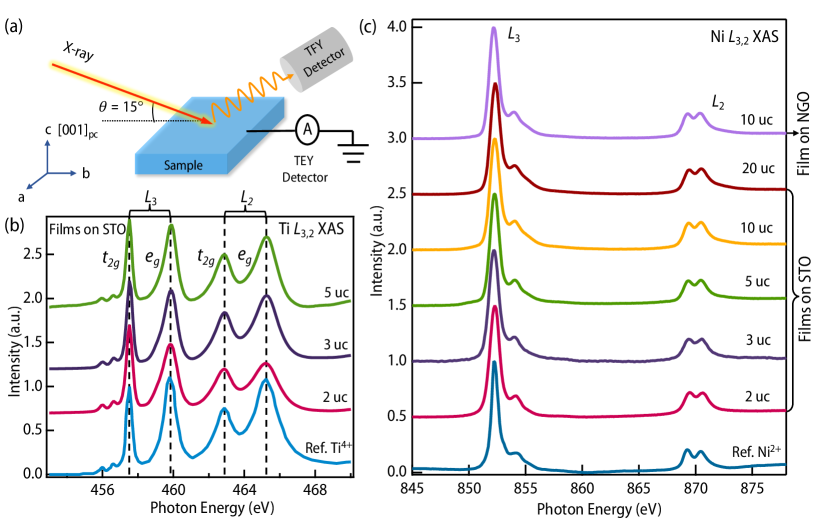
Probing charge compensation on substrate side: The smaller band gap of NNMO (1-1.5 eV) [34, 37] compared to STO (3.25 eV) should result in a straddled band alignment, similar to the well-studied LaMnO3/SrTiO3 (LMO/STO) heterostructure [19, 16, 38, 39, 40, 41]. While in such cases, the electronic reconstruction should occur within the film side of the interface [19, 38], there are also reports of charge compensation within the STO substrates for LMO/STO case [39, 40]. Therefore, it is crucial to probe the electronic structures of both film and substrate as well for NNMO/STO heterostructures. For checking the valence state of the TM sites, we have performed element-sensitive soft X-ray absorption spectroscopy (XAS) experiments for all samples grown on STO and NGO substrates. For a 3 transition metal, the XAS with soft X-ray probes 23 23 transition and the spectral line shape is very sensitive to the valency, spin character of the initial state and crystal field environment of the system [42]. All XAS data, discussed in the main text, were recorded in surface-sensitive total electron yield (TEY) with a grazing incidence geometry (see Fig. 2(a) for experimental arrangement).
The origin of the metallic interface for LAO/STO heterostructure is attributed very often to the polar catastrophe-driven electronic reconstruction mechanism, resulting in Ti3+ in STO near the heterointerface [17]. The presence of oxygen vacancy in STO can also result in metallic behavior due to electron doping on Ti-sites [43]. We start with our attempt to find out any presence of Ti3+ in NNMO/STO heterostructures. As shown in Fig. 2(b), spectral features of Ti L3,2 edges are very similar to that of Ti4+ of bulk stoichiometric STO. On further analyzing the energy separation between the two main peaks of each of the L2 and L3 edges, which are known to detect even small amount of Ti3+ ions [40], we do not find any signature of electron doping on Ti. This is further corroborated by our electrical transport measurements using wire-bonded contacts, which do not find any measurable interfacial conductivity, similar to LaMnO3 /SrTiO3 [19], LaCrO3 /SrTiO3 heterostructures [24]. The presence of any bulk oxygen vacancy within the substrates can also be discarded as all NNMO films were annealed in-situ for 30 minutes under a 500 Torr ultrapure oxygen atmosphere immediately after the deposition.
Probing charge compensation on film side: In the absence of any charge compensation in STO substrate, we proceed to probe toward the film side. In bulk NNMO, Ni has +2 oxidation state, irrespective of any change in the degree of Ni-Mn site-disorder [34, 44]. In Fig. 2(c), we show Ni edge XAS spectra of several films on STO, one 10 uc film on NGO along with a Ni2+ standard: double perovskite Ca2NiOsO6 [36]. Admittedly, Ni remains in Ni2+ state for all films on both substrates, implying that the polar mismatch does not affect Ni ions of NNMO.
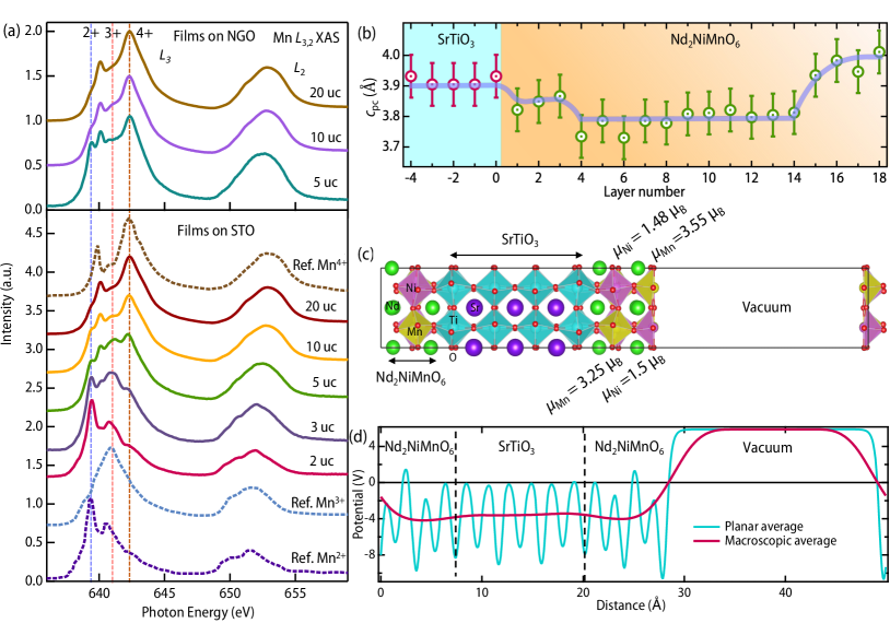
In sharp contrast, we find a systematic change in Mn XAS spectra as shown in Fig. 3(a). For easy comparison, Mn XAS spectra for the standard of Mn2+, Mn3+ and Mn4+ (adapted from Ref. 44), have also been shown in Fig. 3(a). The spectra for 20 uc and 10 uc films on NGO substrate (no interfacial polar mismatch) confirm +4 oxidation state of Mn, similar to bulk NNMO [34]. However, there is a small feature of Mn2+ around 639.4 eV, which becomes much more prominent for the 5 uc film on NGO. On the contrary, there is an additional change in Mn XAS for the films on STO substrate. Apart from the Mn2+ feature which is also found here with a similar trend with the film thickness, an additional feature for Mn3+ states is observed, which increases with the lowering of film thickness. These Mn3+ signatures become comparable to Mn4+ for the 5 uc film and even become the dominant contributor for the 3 uc film. The 2 uc film on STO shows primarily features of Mn2+ and Mn3+. We have also checked Mn XAS of 20 uc NNMO film on NGO and STO in bulk-sensitive total fluorescence (TFY) mode. We do not find any signature of Mn2+ feature there, signifying it is present near the surface (surface contribution is masked by bulk Mn4+ contribution in TFY signal). It may be noted that surface oxygen vacancies leading to Mn2+ ions is very common for manganite thin films [45, 38] and it has also been designated to compensate the polarity for LMO/STO heterostructures [38]. However, such surface Mn2+ cannot compensate for polar catastrophe for NNMO as it is present in films on both STO and NGO substrates. Rather, the compensation is happening through the formation of Mn3+ as it is exclusively present only for films on STO. It is very important to note that the TEY mode probes 4-5 nm length scale from the surface and the contribution of the deeper layers decreases exponentially from the top surface [42]. Thus, the decrease of Mn3+ feature with the increase in NNMO film thickness indicates that the Mn valence is non-uniform along the out-of-plane film direction and there are few layers of the film with a prevailing contribution of Mn3+ ion.
Identifying the regions with dominant contribution of Mn3+ and Mn2+ : The ionic radii of Mn2+, Mn3+ and Mn4+ ions in octahedral environment with high spin configuration are 0.83 Å, 0.645 Å, and 0.53 Å [46]. Thus, the layer-resolved out-of-plane lattice constant () should vary according to the Mn oxidation state if they are in different layers. Fig. 3(b) shows the variation of the layer resolved , evaluated using the HAADF-STEM image, demonstrating film has three types of layers. The of the intermediate layers (4-14 uc from the interface) is very similar to the value obtained from X-ray diffraction measurement (Fig. 1(a), (b)). The higher value of for few outermost layers establishes Mn2+ are indeed located near the film surface. Most importantly, the value for the first three unit cells of the NNMO film is slightly higher, compared to the intermediate layers, implying that 2-3 uc near the interface regions are enriched with Mn3+. Thus, our comprehensive results and detailed analysis from XAS and STEM experiments confirm that site-selective electron doping occurs for interfacial Mn states to compensate for the polar catastrophe in NNMO films on STO. In the forthcoming section, we will discuss in great details regarding the proposed mechanism that deals with this site-selective electron doping in Mn.
Density functional theory: To determine implications of polar catastrophe to the electronic structure, particularly at the interface between the NNNO film and SrTiO3 substrate, we present analysis based on first-principles DFT calculations of bulk STO, bulk NNMO and a symmetric heterostructured slab consisting of 2 uc of NNMO/3.5 uc of STO/2 uc of NNMO Fig. 3(c) (details are provided in the Methods section). Our estimates of the band gap of bulk STO and NNMO are 3.44 eV, and 1.5 eV respectively, which is comparable within the typical DFT errors with the experimental values reported previously [10, 34]. Planar and macroscopic averaged electrostatic potentials of the 2 uc NNMO/3.5 uc STO/ 2 uc NNMO slab (shown in Fig. 3(d)) reveal deviation at the interface from the bulk, reflecting on the mismatch in polarity. The internal electrostatic field obtained as the slope of macroscopic averaged potential is 0.15 V/A, which is comparable to the value reported for the LMO/STO interface [19]. In the self-consistent ground state of the relaxed structure of NNMO:STO:NNMO slab, magnetic moments of Ni ions located at the surface and of those at the film/substrate interface are quite similar. In sharp contrast, Mn ion located at the surface layer has more electrons than the Mn located at the interfacial layer, which is consistent with the Mn2+ observed at the surface from our XAS (Fig. 3(a)) and STEM (Fig. 3(b)) results. Moreover, the calculated electronic structure reveals that (a) the bands near the Fermi energy and of relatively narrow energy width are localized on oxygen atoms at the surface, which correlate with stabilization of oxygen vacancies in the surface layer seen experimentally, and (b) electronic structure projected onto interfacial atoms exhibits a gap, in agreement with experiment.
I Discussion
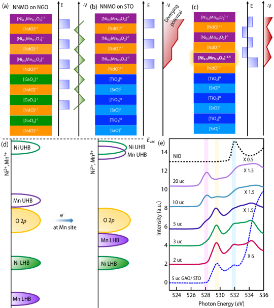
While numerous oxide interfaces with interfacial polar mismatch have been investigated over the last twenty years, the novelty of our work lies in the specific participation of the Mn site and the inertness of the Ni site in the compensation process. Based on our results of extensive XAS and STEM experiments, the following charge compensation [schematically depicted in Fig. 4(a)-(c)] can be considered as a means to alleviate polar catastrophe. The diverging potential for NNMO/STO heterostructure can be compensated by the transfer of 1/2 electron per uc to the interfacial Mn resulting in the formation of Mn3+ cations [22]. It can be easily understood that such electron transfer would be energetically unfavorable if the top layer had Mn4+ akin to bulk NNMO to start with as Mn does not have access to +5 oxidation state. However, some of the surface Mn2+ ions can easily donate electrons and compensate for the polarity mismatch for the NNMO/STO interface. Surprisingly, Ni2+, which is also capable of donating electrons to avoid polar catastrophe [49], remains silent in the present case.
While the potential profile discussed above, based on the ideas initially proposed for semiconductor heterostructures, can account for the polarity compensation in the present case, it fails to explain why only the Mn site takes part in the compensation mechanism. Generally, one would expect electron transfer to occur in any of the transition metal cations present since the potential slope is independent of the nature of the cation. In order to explain such site selectivity, we need to invoke the physics of strong electron correlation for 3 TMOs. In oxygen environment, Ni2+ has a typical value of 6.5 eV and 4 eV [see page 102 of Ref. 47]. The corresponding parameters for Mn4+ are 5 eV and, 1 eV, respectively. In Fig. 4(d), we have drawn the upper Hubbard band (UHB) and lower Hubbard band (LHB) for both Ni2+ and Mn4+ with a common O 2 band. The Mn UHB is at an energetically lower value than the Ni UHB, making it a preferred host to an electron addition. The resultant energy level diagram after the addition of an electron to the Mn is also depicted in Fig. 4(d), highlighting the significant overlap between UHBs of Ni2+ and Mn3+ [ 5 eV and 4 eV for Mn3+, Ref. 47]. Thus, the observed site-selective charge compensation is related to the intrinsic energy scales of correlated physics.
The above modification in unoccupied electronic states is further verified by O -edge XAS measurements. From a pure ionic picture, the dipole transition 12 is forbidden for O2- due to fully filled O 2 shell. However, due to hybridization between TM and O 2 orbitals in real systems, a sizable spectral weight of O 2 is introduced into the unoccupied density of states. This makes O -edge XAS a useful method to find out relative energy positions of cation states above the Fermi level [50]. O -edge XAS spectra for NNMO films on STO substrates have been shown in Fig. 4(e). To identify the features, related to Ti and Ni states, XAS spectra for a 5 uc -Al2O3/SrTiO3 film [51] and bulk NiO [48] have also been plotted. The feature of Ti - O 2 hybridized states of STO substrates are strongly present in the spectra of 5 uc film along with the films with lower thicknesses, and is weakly visible for the 10 uc NNMO film. The feature related to Ni UHB states appears around 532 eV for all NNMO films [48]. The most notable observation is the evolution of the feature around 528 eV with the NNMO film thickness, which is contributed by the Mn -O 2 and Mn -O 2 states [52]. The gradual suppression of this 528 eV peak with the lowering of film thickness establishes the movement of Mn UHB to higher energy, as depicted in Fig. 4(d), due to the charge compensation on Mn sites near the NNMO/STO interfacial regions. This is further supported by our observation that the 528 eV feature remains unaltered with the lowering of NNMO film thickness, grown on NGO substrate.
Conclusion
To summarize, the present study unveils a surprising site-selective charge compensation in Nd2NiMnO6 thin films on SrTiO3 (001) substrates via electron transfer from surface to the interfacial Mn states resulting in Mn3+ cations at the interface. Despite being uniformly distributed as Mn, the Ni sites remain unaffected by the process. By using O K edge XAS, we further demonstrate that this site-selectivity is related to the relative energy position of the upper Hubbard band of Mn4+ with respect to the Ni2+. Thus, our results demonstrate the crucial role and inevitability of strongly correlated electron physics in understanding polar compensation for oxide heterostructures.
More than thousands of double perovskites have been synthesized in the laboratory [28] so far, and we believe such a site-selective charge compensation mechanism will also be pertinent for other insulating double perovskites. Epitaxial stabilization of double perovskites on (111)-oriented perovskite substrates will be another interesting direction to explore as the power of geometrical lattice engineering in realizing novel quantum many-body phases has been demonstrated for simple perovskites [53, 54, 55]. Double perovskites with the desired properties are also being predicted in recent years using machine learning and artificial intelligence [56, 57], and our findings may add another dimension for designing/predicting new double perovskite heterostructures within such an approach.
Methods
Experimental details. Polycrystalline NNMO powder was synthesized using solid-state synthesis [34] and pelletized to make a target for pulsed laser deposition (PLD) growth. TiO2 terminated STO and GaO2-terminated NGO substrates were obtained through thermal annealing of as-received substrates from Shinkosha, Japan [58, 59]. A KrF excimer laser operating at = 248 nm with a fluence of 2 J/cm2 and a repetition rate of 2 Hz was used for the deposition. The growth conditions were maintained the same for films on both STO and NGO substrate, with 150 mTorr dynamic oxygen pressure during the deposition at 750∘C and post-annealing of the films at 500 Torr of oxygen pressure at the same temperature. The layer-by-layer growth with unit cell precision was confirmed by the observation of intensity oscillation of the specular spot of RHEED pattern. The observation of streaks in the RHEED image of the film, taken after cooling to the room temperature, testifies to the smooth surface morphology of the film. Details for GAO/STO sample preparation and characterization can be found in Ref. [51]. XRD and XRR patterns were recorded using a lab-based Rigaku smartlab X-ray diffractometer. Reciprocal space mapping of several films was performed at the 33 ID-D beamline of the Advanced Photon Source (APS), USA with an incident photon energy of 15.5 keV. A spherical aberration-corrected Grand ARM300F operated at 300 kV used for performing STEM and EELS map experiments. XAS measurements were performed in TEY mode at a grazing incidence of 15∘ at the BL 4.0.2 beamline at Advance Light Source, USA. XAS spectra for a few films were also recorded in TFY mode at the 29-ID-D beamline of APS.
Calculation details. Our first-principles calculations are based on density functional theory (DFT) using the SCAN meta-GGA exchange-correlation functional implemented in the VASP code [60, 61, 62]. For bulk NNMO, in order to incorporate the correlation effects of electrons of Nd, electrons of Ni and Mn, we used Hubbard parameters for the mentioned elements as 6 eV, 3.5 eV and 3.5 eV, respectively whereas for STO, the value of was taken to be 8.5 eV for both Sr and Ti. We have chosen these parameters as reported by Chen et al [19]. Spin-polarized DFT was used for all calculations. Projector augmented wave (PAW) potentials were used here, which contain a contribution from kinetic energy density of the core electrons [63]. A kinetic energy cutoff of 600 eV was used to truncate the plane-wave basis for representing wave functions. The Brillouin zone integration was sampled using uniform meshes of k-vectors for estimating optimized lattice parameters of bulk materials. Self-consistent numerical solution of the Kohn-Sham equation was obtained iteratively to converge total energy within 10-5 eV. We relaxed the structures to minimize the energy until the Hellman-Feynman forces on each atom was less than 0.002 eV/Å.
With the optimized lattice parameters obtained for bulk materials, we simulated the NNMO/ STO /NNMO heterostructure. The unit cell of cubic bulk STO was doubled in plane (lattice parameters and ) first and then made thrice the thickness of it along lattice parameter . The top and bottom of the STO slabs were terminated with extra TiO2 layers along (100) direction. These TiO2 layers were interfaced with (110)or surface of NNMO with thickness of 2 uc at top and bottom of the heterostructure. The heterostructure was simulated in a manner such that the top and bottom atomic layers of NNMO are placed with symmetry (as a mirror image of each other) keeping STO in the middle of the heterostructure. We further relaxed the heterostructure. The Brillouin zone integration was sampled over uniform meshes of . The vacuum layer was taken about 23 Å along vector to separate between two successive slabs in the simulation cell.
Acknowledgement
The authors acknowledge XRD and wire bonding facilities of the Department of Physics, IISc Bangalore. SM acknowledges funding support from a SERB Core Research grant (Grant No. CRG/2022/001906). SM would also like to acknowledge the seed funding from Quantum Research Park (QuRP), funded by Karnataka Innovation and Technology Society (KITS), K-Tech, Government of Karnataka. NB acknowledges funding from the Prime Minister’s Research Fellowship (PMRF), MoE, Government of India. JM acknowledges UGC, India for fellowship. This research used resources of the Advanced Photon Source, a U.S. Department of Energy Office of Science User Facility operated by Argonne National Laboratory under Contract No. DE-AC02-06CH11357. This research used resources of the Advanced Light Source, which is a Department of Energy Office of Science User Facility under Contract No. DE-AC02-05CH11231. ZY acknowledges the National Natural Science Foundation of China (Grant No. 52202235).
References
- [1] Tsymbal, E. Y., Dagotto, E. R., Eom, C.-B. & Ramesh, R. Multifunctional oxide heterostructures (OUP Oxford, 2012).
- [2] Frensley, W. R. & Kroemer, H. Theory of the energy-band lineup at an abrupt semiconductor heterojunction. Phys. Rev. B 16, 2642–2652 (1977). URL https://link.aps.org/doi/10.1103/PhysRevB.16.2642.
- [3] Harrison, W. A., Kraut, E. A., Waldrop, J. R. & Grant, R. W. Polar heterojunction interfaces. Phys. Rev. B 18, 4402–4410 (1978). URL https://link.aps.org/doi/10.1103/PhysRevB.18.4402.
- [4] Frensley, W. R. & Kroemer, H. Interstitial potential differences, electronegativity differences, and effective ionic charges in zinc‐blende‐type semiconductors. Applied Physics Letters 31, 48–50 (1977). URL https://doi.org/10.1063/1.89475.
- [5] Grant, R. W., Waldrop, J. R. & Kraut, E. A. Observation of the orientation dependence of interface dipole energies in ge-gaas. Phys. Rev. Lett. 40, 656–659 (1978). URL https://link.aps.org/doi/10.1103/PhysRevLett.40.656.
- [6] Pollmann, J. & Mazur, A. Theory of semiconductor heterojunctions. MRS Online Proceedings Library (OPL) 18, 257 (1982).
- [7] Hwang, H. Y. et al. Emergent phenomena at oxide interfaces. Nature Materials 11, 103–113 (2012). URL https://doi.org/10.1038/nmat3223.
- [8] Chakhalian, J., Freeland, J. W., Millis, A. J., Panagopoulos, C. & Rondinelli, J. M. Colloquium: Emergent properties in plane view: Strong correlations at oxide interfaces. Rev. Mod. Phys. 86, 1189–1202 (2014). URL https://link.aps.org/doi/10.1103/RevModPhys.86.1189.
- [9] Middey, S. et al. Physics of ultrathin films and heterostructures of rare-earth nickelates. Annual Review of Materials Research 46, 305–334 (2016). URL https://doi.org/10.1146/annurev-matsci-070115-032057.
- [10] Ohtomo, A. & Hwang, H. Y. A high-mobility electron gas at the laalo3/srtio3 heterointerface. Nature 427, 423–426 (2004). URL https://doi.org/10.1038/nature02308.
- [11] Stemmer, S. & James Allen, S. Two-dimensional electron gases at complex oxide interfaces. Annual Review of Materials Research 44, 151–171 (2014). URL https://doi.org/10.1146/annurev-matsci-070813-113552.
- [12] Reyren, N. et al. Superconducting interfaces between insulating oxides. Science 317, 1196–1199 (2007).
- [13] Bert, J. A. et al. Direct imaging of the coexistence of ferromagnetism and superconductivity at the laalo3/srtio3 interface. Nature Physics 7, 767–771 (2011). URL https://doi.org/10.1038/nphys2079.
- [14] Li, L., Richter, C., Mannhart, J. & Ashoori, R. C. Coexistence of magnetic order and two-dimensional superconductivity at laalo3/srtio3 interfaces. Nature Physics 7, 762–766 (2011). URL https://doi.org/10.1038/nphys2080.
- [15] Lee, J.-S. et al. Titanium dxy ferromagnetism at the laalo3/srtio3 interface. Nature materials 12, 703–706 (2013).
- [16] Anahory, Y. et al. Emergent nanoscale superparamagnetism at oxide interfaces. Nature Communications 7, 12566 (2016). URL https://doi.org/10.1038/ncomms12566.
- [17] Nakagawa, N., Hwang, H. Y. & Muller, D. A. Why some interfaces cannot be sharp. Nature Materials 5, 204–209 (2006). URL https://doi.org/10.1038/nmat1569.
- [18] Takizawa, M. et al. Spectroscopic evidence for competing reconstructions in polar multilayers laalo 3/lavo 3/laalo 3. Physical Review Letters 102, 236401– (2009). URL https://link.aps.org/doi/10.1103/PhysRevLett.102.236401.
- [19] Chen, Z. et al. Electron accumulation and emergent magnetism in heterostructures. Phys. Rev. Lett. 119, 156801 (2017). URL https://link.aps.org/doi/10.1103/PhysRevLett.119.156801.
- [20] Park, J. et al. Oxygen-vacancy-induced orbital reconstruction of ti ions at the interface of heterostructures: A resonant soft-x-ray scattering study. Phys. Rev. Lett. 110, 017401 (2013). URL https://link.aps.org/doi/10.1103/PhysRevLett.110.01740.
- [21] Middey, S. et al. Polarity compensation in ultra-thin films of complex oxides: The case of a perovskite nickelate. Scientific Reports 4, 6819 (2014). URL https://doi.org/10.1038/srep06819.
- [22] Mundy, J. A. et al. Visualizing the interfacial evolution from charge compensation to metallic screening across the manganite metal–insulator transition. Nature communications 5, 3464 (2014).
- [23] De Luca, G. et al. Top-layer engineering reshapes charge transfer at polar oxide interfaces. Advanced Materials 34, 2203071 (2022).
- [24] Chambers, S. A. et al. Band alignment, built-in potential, and the absence of conductivity at the heterojunction. Phys. Rev. Lett. 107, 206802 (2011). URL https://link.aps.org/doi/10.1103/PhysRevLett.107.206802.
- [25] Salluzzo, M. et al. Structural and electronic reconstructions at the laalo3/srtio3 interface. Advanced Materials 25, 2333–2338 (2013). URL https://doi.org/10.1002/adma.201204555.
- [26] Goodge, B. H. et al. Resolving the polar interface of infinite-layer nickelate thin films. Nature Materials 22, 466–473 (2023).
- [27] Zaanen, J., Sawatzky, G. A. & Allen, J. W. Band gaps and electronic structure of transition-metal compounds. Phys. Rev. Lett. 55 (1985). URL https://link.aps.org/doi/10.1103/PhysRevLett.55.418.
- [28] Vasala, S. & Karppinen, M. A2bbo6 perovskites: A review. Progress in Solid State Chemistry 43, 1–36 (2015). URL https://www.sciencedirect.com/science/article/pii/S0079678614000338.
- [29] Sarma, D., Mahadevan, P., Saha-Dasgupta, T., Ray, S. & Kumar, A. Electronic structure of sr2femoo6. Phys Rev Lett 85, 2549–2552 (2000). URL https://link.aps.org/doi/10.1103/PhysRevLett.85.2549.
- [30] Kobayashi, K.-I., Kimura, T., Sawada, H., Terakura, K. & Tokura, Y. Room-temperature magnetoresistance in an oxide material with an ordered double-perovskite structure. Nature 395, 677–680 (1998). URL https://doi.org/10.1038/27167.
- [31] Choudhury, D. et al. Near-room-temperature colossal magnetodielectricity and multiglass properties in partially disordered . Phys. Rev. Lett. 108, 127201 (2012). URL https://link.aps.org/doi/10.1103/PhysRevLett.108.127201.
- [32] Rogado, N. S., Li, J., Sleight, A. W. & Subramanian, M. A. Magnetocapacitance and magnetoresistance near room temperature in a ferromagnetic semiconductor: La2nimno6. Advanced Materials 17, 2225–2227 (2005). URL https://doi.org/10.1002/adma.200500737.
- [33] Saha-Dasgupta, T. Double perovskites with 3d and 4d/5d transition metals: compounds with promises. Materials Research Express 7, 014003 (2020).
- [34] Pal, S. et al. Peculiar magnetic states in the double perovskite . Phys. Rev. B 100, 045122 (2019). URL https://link.aps.org/doi/10.1103/PhysRevB.100.045122.
- [35] Spurgeon, S. R. et al. Onset of phase separation in the double perovskite oxide . Phys. Rev. B 97, 134110 (2018). URL https://link.aps.org/doi/10.1103/PhysRevB.97.134110.
- [36] Morrow, R. et al. Magnetism in ca2cooso6 and ca2nioso6: Unraveling the mystery of superexchange interactions between 3d and 5d ions. Chemistry of Materials 28, 3666–3675 (2016).
- [37] Nasir, M. et al. Role of antisite disorder, rare-earth size, and superexchange angle on band gap, curie temperature, and magnetization of r2nimno6 double perovskites. ACS Applied Electronic Materials 1, 141–153 (2019).
- [38] Kaspar, T. C. et al. Electronic structure and band alignment of lamno3/srtio3 polar/nonpolar heterojunctions. Advanced Materials Interfaces 6, 1801428 (2019). URL https://doi.org/10.1002/admi.201801428.
- [39] Garcia-Barriocanal, J. et al. “charge leakage” at lamno3/srtio3 interfaces. Advanced Materials 22, 627–632 (2010).
- [40] Garcia-Barriocanal, J. et al. Spin and orbital ti magnetism at lamno3/srtio3 interfaces. Nature Communications 1, 82 (2010). URL https://doi.org/10.1038/ncomms1080.
- [41] Wang, X. R. et al. Imaging and control of ferromagnetism in lamno3/srtio3 heterostructures. Science 349, 716–719 (2015). URL https://doi.org/10.1126/science.aaa5198.
- [42] Stöhr, J. & Siegmann, H. C. Magnetism. Solid-State Sciences. Springer, Berlin, Heidelberg 5, 236 (2006).
- [43] Herranz, G. et al. High mobility in heterostructures: Origin, dimensionality, and perspectives. Phys. Rev. Lett. 98, 216803 (2007). URL https://link.aps.org/doi/10.1103/PhysRevLett.98.216803.
- [44] Pal, S. et al. Effect of anti-site disorder on magnetism in . Phys. Rev. B 97, 165137 (2018). URL https://link.aps.org/doi/10.1103/PhysRevB.97.165137.
- [45] Calderón, M. J., Brey, L. & Guinea, F. Surface electronic structure and magnetic properties of doped manganites. Phys. Rev. B 60, 6698–6704 (1999). URL https://link.aps.org/doi/10.1103/PhysRevB.60.6698.
- [46] Shannon, R. D. Revised effective ionic radii and systematic studies of interatomic distances in halides and chalcogenides. Acta crystallographica section A: crystal physics, diffraction, theoretical and general crystallography 32, 751–767 (1976).
- [47] Khomskii, D. Transition metal compounds (Cambridge University Press, 2014).
- [48] Kuiper, P., Kruizinga, G., Ghijsen, J., Sawatzky, G. A. & Verweij, H. Character of holes in and their magnetic behavior. Phys. Rev. Lett. 62, 221–224 (1989). URL https://link.aps.org/doi/10.1103/PhysRevLett.62.221.
- [49] Tung, I.-C. et al. Polarity-driven oxygen vacancy formation in ultrathin films on . Phys. Rev. Mater. 1, 053404 (2017). URL https://link.aps.org/doi/10.1103/PhysRevMaterials.1.053404.
- [50] Frati, F., Hunault, M. O. & De Groot, F. M. Oxygen k-edge x-ray absorption spectra. Chemical reviews 120, 4056–4110 (2020).
- [51] Ojha, S. K. et al. Electron trapping and detrapping in an oxide two-dimensional electron gas: The role of ferroelastic twin walls. Phys. Rev. Appl. 15, 054008 (2021). URL https://link.aps.org/doi/10.1103/PhysRevApplied.15.054008.
- [52] Galdi, A. et al. Electronic band redistribution probed by oxygen absorption spectra of (srmno3)n(lamno3)2n superlattices. Phys. Rev. B 85, 125129 (2012). URL https://link.aps.org/doi/10.1103/PhysRevB.85.125129.
- [53] Liu, X., Middey, S., Cao, Y., Kareev, M. & Chakhalian, J. Geometrical lattice engineering of complex oxide heterostructures: a designer approach to emergent quantum states. MRS Communications 6, 133–144 (2016).
- [54] Middey, S. et al. Mott electrons in an artificial graphenelike crystal of rare-earth nickelate. Phys. Rev. Lett. 116, 056801 (2016). URL https://link.aps.org/doi/10.1103/PhysRevLett.116.056801.
- [55] Kim, T. et al. Polar metals by geometric design. Nature 533, 68–72 (2016).
- [56] Pilania, G. et al. Machine learning bandgaps of double perovskites. Scientific reports 6, 19375 (2016).
- [57] Tao, Q., Xu, P., Li, M. & Lu, W. Machine learning for perovskite materials design and discovery. npj Computational Materials 7, 23 (2021).
- [58] Kumar, S. et al. Electronic and magnetic properties of epitaxial thin film of nd0. 5ba0. 5mno3. Applied Physics Letters 120, 061602 (2022).
- [59] Patel, R. K. et al. Thickness dependent OER electrocatalysis of epitaxial thin film of high entropy oxide. Applied Physics Reviews 10, 031407 (2023). URL https://doi.org/10.1063/5.0146005. eprint https://pubs.aip.org/aip/apr/article-pdf/doi/10.1063/5.0146005/18068792/031407_1_5.0146005.pdf.
- [60] Sun, J., Ruzsinszky, A. & Perdew, J. P. Strongly constrained and appropriately normed semilocal density functional. Phys. Rev. Lett. 115, 036402 (2015). URL https://link.aps.org/doi/10.1103/PhysRevLett.115.036402.
- [61] Kresse, G. & Furthmüller, J. Efficient iterative schemes for ab initio total-energy calculations using a plane-wave basis set. Phys. Rev. B 54, 11169–11186 (1996). URL https://link.aps.org/doi/10.1103/PhysRevB.54.11169.
- [62] Kresse, G. & Furthmüller, J. Efficiency of ab-initio total energy calculations for metals and semiconductors using a plane-wave basis set. Computational Materials Science 6, 15–50 (1996). URL https://www.sciencedirect.com/science/article/pii/0927025696000080.
- [63] Kresse, G. & Joubert, D. From ultrasoft pseudopotentials to the projector augmented-wave method. Phys. Rev. B 59, 1758–1775 (1999). URL https://link.aps.org/doi/10.1103/PhysRevB.59.1758.