Suppression of thermal smearing in a feedback-driven atomic size Josephson junction
The ultimate spatial limit to establish a Josephson coupling between two superconducting electrodes is an atomic-scale vacuum tunneling junction. The Josephson effect in such ultrasmall junctions has been widely used to study superconducting materials, providing a powerful probe of the spatial variations of the superfluid density. Furthermore, studies of the supercurrent and charging effects unveiled new, frequency dependent, switching dynamics and thermal processes emerging due to the small size of the junctions. However, the Cooper pair current magnitude was considerably reduced by thermal fluctuations. Here we show that a feedback element induces a time-dependent bistable regime which periodically restores the zero voltage state. We find that the time-averaged current within the bistable regime is independent of thermal smearing, opening new avenues to study superconducting phenomena at the nanoscale.
Main
Atomic-scale superconducting Josephson junctions are highly susceptible to phase fluctuations due to their small size. For small typical junctions in Al or Pb (with critical temperature Tc of 1.2 K and 7.2 K respectively), the critical current is often small, in the nA range, and the Josephson coupling energy ( being the flux quantum) can fall down to the mK range. Thus, even at temperatures well below Tc, there are significant thermal fluctuations of the superconducting phase, which suppress the Josephson current.
To see how to address the problem of thermal fluctuations in Josephson junctions, we start by discussing the standard resistively and capacitively shunted junction (RCSJ) model, shown in Fig. 1a (black lines) [1]. The bias current can be separated through Kirchoff’s law into the sum of the supercurrent through the junction (from the first Josephson relation, is the phase difference across the junction), the current through a resistance (following the second Josephson relation, a resistive voltage drop at the junction corresponds to a current , with the resistance), and the current through a capacitance (given by . Thermal phase fluctuations induce a time dependence of the phase difference , whose influence in the circuit can be reduced by designing the electromagnetic environment to obtain large damping, for instance through a large impedance [2, 3, 4, 5]. However, it is not always feasible to modify damping, for instance in Josephson junctions made with a Scanning Tunneling Microscope (STM).
Scanning Josephson spectroscopy (SJS) probes superconducting samples using a superconducting STM tip while recording the near-zero voltage current with atomic precision. This requires a vacuum atomic size junction, which essentially fixes to the inverse of the vacuum impedance shuntimg the circuit at high frequency, and to the capacitance between tip and sample. Even with reduced Josephson currents, SJS has contributed to the understanding of pair density waves in cuprates and chalcogenides [6, 7], inhomogeneous superconductivity in pnictides [8], photon assisted Cooper pair tunneling [9], individual bound states tunneling [10], or a diode effect [11]. However, in these and other small scale Josephson junctions the avoidable reduced Josephson current poses a considerable limitation for further studies[12, 13].
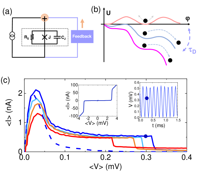
A route to reduce thermal fluctuations is to use a delayed and time dependent feedback [14, 15, 16]. To understand the effect of a feedback on a Josephson junction, we recall that behaves as the position of a particle in a one dimensional potential . We can write . has the form of a tilted washboard as shown in Fig. 1b [17]. With a small (orange curve in Fig. 1b), the phase difference remains around a potential minimum, resulting in zero voltage across the junction. As the bias is increased (blue and magenta curves), the phase rolls down the potential, leading to a non-zero voltage. A feedback adds a time delayed current to the actual Josephson current and periodically inhibits the evolution of the phase with time by reducing the tilt, as schematically shown in Fig. 1a,b. As we show below, thermal phase fluctuations are suppressed through a time dependent oscillatory action on the circuit.
Feedback driven Josephson junction
In Fig. 1c, we compare a time-averaged current-voltage characteristic for a Josephson junction formed between a Pb STM tip and a Pb sample (blue line) when a feedback element is integrated into the circuit, to the result obtained without a feedback element (dashed blue line, the experiment is described below and in Methods). We observe a regime with a sustained current in the circuit with a feedback over a bias range that is considerably larger than in the circuit without a bias. As we show in the upper right inset the voltage fluctuates with time in this regime. Importantly, whereas the behavior close to zero bias is highly temperature dependent (following approximately the same behavior as in the circuit without a feedback), the current in the regime induced by the feedback is almost independent of temperature.
To gain a deeper understanding, let us start by establishing the feedback RCSJ model at zero temperature. We can write
| (1) |
where is given by
| (2) |
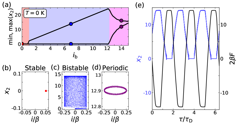
Here, and are the dimensionless variables, the reduced time is , with the characteristic Josephson time (and the Josephson frequency), the reduced bias current is , and is the McCumber parameter. Eq. 1 corresponds to the conventional RCSJ model plus the feedback term . is the bandwidth of the measurement circuit. The behavior of the solutions to the new coupled equations and Eq. (1) is shown in Fig. 2.
In Fig. 2 we show the evolution of voltage as function of the bias current. We identify three distinct regimes. For (orange in Fig. 2a and Fig. 2b) we find zero voltage, , and a finite Josephson current . When , and . The feedback reacts and there is an increase of up to . The current through the junction first increases and then oscillates at a time scale which is of order of . After a time , becomes too, which drives down to through the feedback (blue in Fig. 2a and Fig. 2c). The reaction of the feedback is immediate for but requires more time when increases. As an example we show the evolution of the voltage and the current with time in Fig. 2c over one period of the feedback approximately in the middle of the bistable regime. We see an initial increase in with and then an increase of to . We show the time dependence of and of in Fig. 2e. The establishment of the feedback (periods with a finite slope in Fig. 2e) gradually takes over more time when increases. Ultimately, when the required time reaches we lose the bistable regime and find the conventional AC periodic Josephson regime, characterized by a finite time-averaged voltage and a zero time-averaged current (blue in Fig. 2a and Fig. 2d). When decreasing again, , for which the feedback (Eq. 2) remains low over a certain range of , so that a smaller is needed to reach the bistable regime, obtaining a hysteretic behavior.
We note that the time-averaged current just at the point where the bistable regime is lost, is propotional to . At this point, the time dependence of (Fig. 2e) is close to a triangular wave, such that there is indeed just a single unit in time for which is not oscillating and does not average to zero. As we show below, this point is asymptotically approached when increasing within the bistable regime, giving a time-averaged current which is independent of thermal smearing.
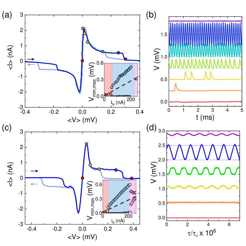
We now compare theory and experiment at a finite temperature. In Fig. 3a, we show a time-averaged current-voltage characteristic taken on an atomic size tunnel junction between a tip and a sample of Pb ( K and meV, s. Starting from zero bias, we observe that the average current increases, reaches a peak, and then decreases and saturates at a plateau, eventually dropping to zero at higher bias voltages. The point at which the current drops to zero is hysteretic and depends on the direction of the bias voltage ramp (light and dark blue lines show the different ramping directions). The time dependence of the voltage is shown in Fig. 3b and the minimum and maximum values in the inset of Fig. 3a (we use s for the temporal range or bandwidth of the experimental set-up, see also Methods). We observe a bistable regime (orange to blue curves) where the junction switches periodically, approximately every ms, between zero and a finite voltage. In Fig. 3c we show the time-averaged current vs voltage resulting from our simulations. The voltage vs time is shown in Fig. 3d and the minimum and maximum values in the inset of Fig. 3c. We see that experiment and calculations are mostly identical. The shape of the time-averaged current to voltage curve is similar, the hysteresis has a similar shape and the oscillatory behavior in the bistable regime occurs in experiment as well as in simulations.
Increasing the temperature reduces both the bistable range as well as the size of the hysteretic behavior, but leads, as shown in Extended Data Fig. 1, to a temperature independent value of the time-averaged current in the bistable regime.
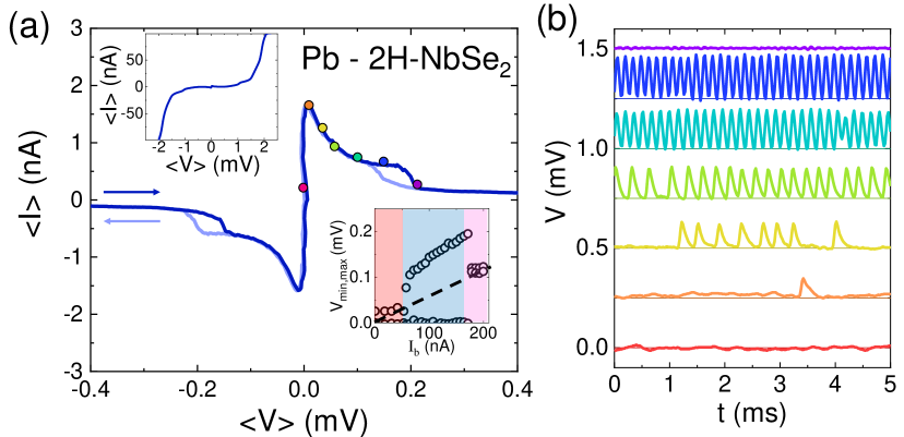
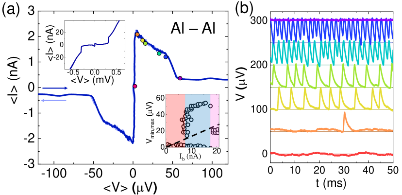
A detailed analysis of the different parameters governing the feedback RCSJ model (Extended Data Fig. 2 and Methods) shows that the appearance of the bistable regime for different time constants goes all the way down to being one or two orders of magnitude larger than . Furthermore, there is a large range of where the bistable regime can be observed. On the other hand, should be smaller than , but below , the integration does no longer provide a sufficiently large feedback term. In the experiment, we have observed the bistable regime in Pb-NbSe2 and in Al-Al atomic size junctions (Extended Data Figs. 3,4 and Supplementary Information). We discuss the dependence on the circuit parameters in Methods (circuit is shown in Extended Data Fig. 5). The switching behavior between different regimes is thermally driven, as shown in the Extended Data Fig. 6 and discussed in the Supplementary Information.
Note that there is a discrepancy between the symmetric peaks obtained in the voltage as a function of time in the bistable regime of our simulations, and the asymmetric peaks observed in the experiment (yellow and green curves in Fig. 3b and Fig. 3d). We do not have a clear explanation for this discrepancy, but it might be related to asymmetries in the circuit. For instance, different resistance and capacitance values in the two branches connecting the junction (Fig. 1c), which are not included in our feedback RCSJ model. The other essential features, such as the existence of a bistable regime and its accompanying hysteretic behavior, are accurately captured by the feedback RCSJ model.
Critical current from the bistable regime in feedback driven ultra small Josephson junctions
In summary, we have unveiled a novel behavior in ultrasmall Josephson junctions when measured with a circuit that incorporates a delayed feedback element. This component can induce bistable oscillations between two distinct states: the conventional one characterized by zero voltage and a finite Josephson current, and a non-zero voltage state. Notice that the observed delay time in the experiments is dictated by the time constant of the feedback component while is provided by the bandwidth of the experimental set-up.
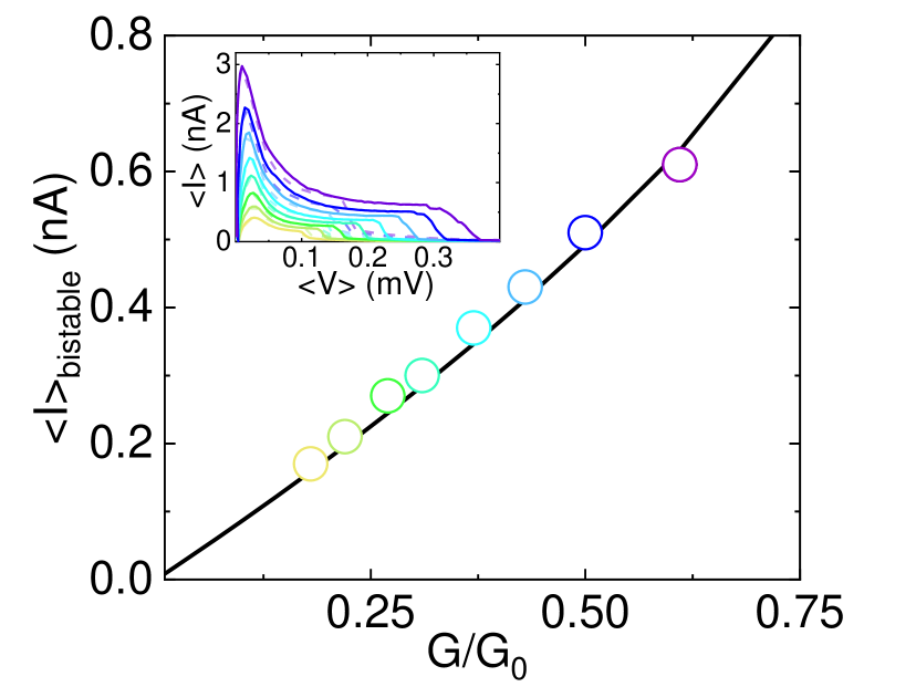
From the feedback RCSJ model at a finite temperature, we find that in the bistable regime, just before the transition to the periodic regime. This is in sharp contrast to the value of the current close to zero voltage, for , which decreases with increasing temperature as , or with the derivative of the current near zero voltage, which decreases with temperature as (see Supplementary Information). For the experiment shown in Fig. 3a, we find nA, which is very similar to the estimation provided by the Ambegaokar-Baratoff equation for symmetric junctions at zero temperature [18] ( being the conductance and the quantum of conductance, we use and meV). By taking and nA we can follow closely the dependence of on , as shown in Fig. 4, finding that the experiment (dots) follows the calculations (line). Thus, the measurement of the time-averaged current in the bistable regime provides a quantitative measurement of the critical current of the junction.
The bistable regime is found in junctions with different superconductors, as shown in the Supplementary Information. It is worth pointing out that performing SJS in the bistable regime can be particularly interesting when measuring a topological superconductor [19, 20, 21, 22, 23, 24, 25, 26, 27] or a chain of magnetic adatoms [28, 29]. In such systems, the phase coherent tunneling between the s-wave state of the tip and p-wave state of the sample occurs through higher-order processes [26], which considerably reduces the zero-bias Josephson current. Our method enables the sampling of the (near-zero) Josephson effect over a larger range of voltages, and allows to better probe the spatial distribution of the topologically protected states. The implications of our findings extend further, offering new possibilities for the measurement of small-size Josephson junctions through the detection of a signal which is mostly free of thermal broadening.
References
- [1] Gross, R. & Deppe, F. Josephson effect and superconducting electronics (Walter De Gruyter Incorporated, 2016, 2016).
- [2] Tinkham, M. & Tinkham, M. Introduction to Superconductivity (Dover Publications INC, 2004).
- [3] Goffman, M. F., Cron, R., Levy Yeyati, A., Joyez, P. & Devoret, M. H., Esteve, D. & Urbina, C. Supercurrent in atomic point contacts and Andreev states. Phys. Rev. Lett. 85, 170 (2000).
- [4] Vion, D., Götz, M., Joyez, P., Esteve, D. & Devoret, M. H. Thermal activation above a dissipation barrier: Switching of a small Josephson junction. Phys. Rev. Lett. 77, 3435–3438 (1996).
- [5] Joyez, P., Vion, D., Götz, M., Devoret, M. H. & Esteve, D. The Josephson effect in nanoscale tunnel junctions. Journal of Superconductivity 12, 757–766 (1999).
- [6] Hamidian, M. H. et al. Detection of a Cooper-pair density wave in Bi2Sr2CaCu2O8+x. Nature 532, 343–347 (2016).
- [7] Liu, X., Chong, Y. X., Sharma, R. & Davis, J. C. S. Discovery of a Cooper-pair density wave state in a transition-metal dichalcogenide. Science 372, 1447–1452 (2021).
- [8] Cho, D., Bastiaans, K. M., Chatzopoulos, D., Gu, G. D. & Allan, M. P. A strongly inhomogeneous superfluid in an iron-based superconductor. Nature 571, 541–545 (2019).
- [9] Jäck, B. et al. Quantum Brownian motion at strong dissipation probed by superconducting tunnel junctions. Phys. Rev. Lett. 119, 147702 (2017).
- [10] Huang, H. et al. Tunnelling dynamics between superconducting bound states at the atomic limit. Nature Physics 16, 1227–1231 (2020).
- [11] Trahms, M. et al. Diode effect in Josephson junctions with a single magnetic atom. Nature 615, 628–633 (2023).
- [12] Lee, G.-H. et al. Graphene-based Josephson junction microwave bolometer. Nature 586, 42–46 (2020).
- [13] Subero, D. et al. Bolometric detection of coherent Josephson coupling in a highly dissipative environment (2022). ArxiV:2210.14953.
- [14] Gregorio, P. D., Rondoni, L., Bonaldi, M. & Conti, L. Harmonic damped oscillators with feedback: a Langevin study. Journal of Statistical Mechanics: Theory and Experiment 2009, P10016 (2009).
- [15] Brown, K. R. et al. Passive cooling of a micromechanical oscillator with a resonant electric circuit. Phys. Rev. Lett. 99, 137205 (2007).
- [16] Cohadon, P. F., Heidmann, A. & Pinard, M. Cooling of a mirror by radiation pressure. Phys. Rev. Lett. 83, 3174–3177 (1999).
- [17] Chesca, B., Kleiner, R. & Koelle, D. SQUID Theory, chap. 2, 29–92 (John Wiley and Sons Ltd, 2005).
- [18] Ambegaokar, V. & Baratoff, A. Tunneling between superconductors. Phys. Rev. Lett. 10, 486–489 (1963).
- [19] Strand, J. D., Van Harlingen, D. J., Kycia, J. B. & Halperin, W. P. Evidence for complex superconducting order parameter symmetry in the low-temperature phase of UPt3 from Josephson interferometry. Phys. Rev. Lett. 103, 197002 (2009).
- [20] Lutchyn, R. M., Sau, J. D. & Das Sarma, S. Majorana fermions and a topological phase transition in semiconductor-superconductor heterostructures. Phys. Rev. Lett. 105, 077001 (2010).
- [21] Oreg, Y., Refael, G. & von Oppen, F. Helical liquids and Majorana bound states in quantum wires. Phys. Rev. Lett. 105, 177002 (2010).
- [22] Fu, L. & Berg, E. Odd-parity topological superconductors: Theory and application to CuxBi2Se3. Phys. Rev. Lett. 105, 097001 (2010).
- [23] Graham, M. & Morr, D. K. Imaging the spatial form of a superconducting order parameter via Josephson scanning tunneling spectroscopy. Phys. Rev. B 96, 184501 (2017).
- [24] Cornils, L. et al. Spin-resolved spectroscopy of the Yu-Shiba-Rusinov states of individual atoms. Phys. Rev. Lett. 119, 197002 (2017).
- [25] Escribano, S. D., Levy Yeyati, A., Oreg, Y. & Prada, E. Effects of the electrostatic environment on superlattice Majorana nanowires. Phys. Rev. B 100, 045301 (2019).
- [26] Zazunov, A., Iks, A., Alvarado, M., Levy Yeyati, A. & Egger, R. Josephson effect in junctions of conventional and topological superconductors. Beilstein Journal of Nanotechnology 9, 1659–1676 (2018).
- [27] Heinrich, B. W., Pascual, J. I. & Franke, K. J. Single magnetic adsorbates on s-wave superconductors. Progress in Surface Science 93, 1–19 (2018).
- [28] Nadj-Perge, S. et al. Observation of Majorana fermions in ferromagnetic atomic chains on a superconductor. Science 346, 602–607 (2014).
- [29] Schneider, L. et al. Probing the topologically trivial nature of end states in antiferromagnetic atomic chains on superconductors. Nature Communications 14, 2742 (2023).
Methods
Temperature dependence in the feedback-driven RCSJ model
We model the experiments through a feedback-driven RCSJ model following Refs. [1, 2]. By using the Kirchhoff equations on the circuit of Fig. 1b and introducing the feedback term and thermal noise, we obtain the set of differential equations
| (3) | ||||
| (4) |
The first equation corresponds to the voltage drop through the circuit while the second one accounts for the total current. The first term in the second equation is the current bias and the second one is the feedback term. This term compares the voltage at two different times, and , and adds to the circuit, multiplied by a coupling constant that has units of inverse resistance. Since the feedback element may not allow for a full resolution of , we introduce an average for time-scales . The third term gives the current through the Josephson junction, with the critical current and the phase difference. The fourth and fifth terms provide the currents through the resistance and the capacitor , respectively. The last term simulates the current fluctuations in the junction as a result of thermal noise, with the temperature and a time-dependent function that provides normally distributed random values that average to zero with standard deviation of one. This term is modeled following Ref. [2], which offers an expression especially suitable for Runge-Kutta solvers ( is the time discretization).
We can now rewrite the set of first-order differential equations of Eqs. (3) and (4) as a (dimensionless) second-order differential equation
| (5) |
where is the reduced time (with the inverse of the characteristic Josephson frequency), the McCumber parameter, and the reduced bias current. Notice that and are also written in units of .
Defining and , we can write
| (6) |
This equation is equivalent to Eq. (1) of the main text but including the effect of a finite temperature through a white noise term. Moreover, we assume in the main text perfect coupling between the feedback element and the circuit, provided by , in which the feedback perfectly compensates the voltage drop through the circuit (at ).
We solve this non-linear delayed differential equation using a fourth-order Runge-Kutta method as a function of time and sweeping for different bias current . For each current bias , we impose as initial condition the values of found for the previous value of . In this way we obtain a hysteretic behavior as also found in the experiments. We employ a small time discretization step so that the time scale is well-resolved () and we compute the solution for very large time scales so that one can account for the phenomena happening at scales of . Notice that there are five orders of magnitude between and , which makes these simulations computationally challenging.
Once and are found we compute the current and voltage through the Josephson junction as
| (7) |
and find their time average and . We remove the initial solutions to the differential equation in the time average (a few intervals) as the simulations may take some time to reach a possible different regime when changing . We also run several times (10 times) the same simulation using the same and initial condition, and average among the solutions to remove the dependence on a particular realization of thermal noise.
Parameters of the feedback-driven RCSJ model
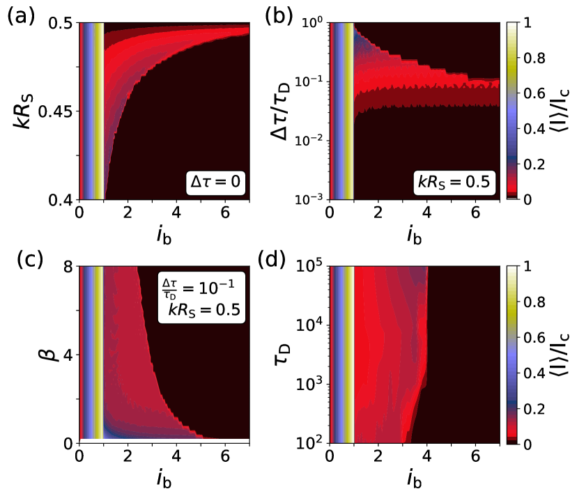
To explore the impact of different parameters of the feedback on the results of the model we calculate the time-averaged current for different bias currents and parameters: (shown in Extended Data Figure 2a, is given by the color scale), (Extended Data Figure 2b), (Extended Data Figure 2c) and (Extended Data Figure 2d) at zero temperature. In the stable regime, (Extended Data Figure 2a), the coupling constant has no significant influence since the feedback does not play a significant role. However, for we observe a substantial bistable regime that appears within the range of approximately to , as indicated by the red area in Extended Data Figure 2a (red indicates a finite , see color scale on the right). The saddle points of the differential equation determine the bistablility regime, which follows in this case . There is a divergence at , which serves as the upper boundary for the bistablility range. Conversely, the lower boundary for is when . Below this value the range for the bistable regime is infinitesimally close to the stable regime. In the present simulation this occurs at approximately .
The effect of the integration interval is very similar to that of as it ultimately modifies the coupling between and an average near . Thus, even at perfect coupling , see Extended Data Figure 2b, the bistability is possible when is smaller than the characteristic delay time , as is averaged to a very different quantity. Notice, nevertheless, that the bistable regime disappears when , as the feedback element averages to a time-independent constant.
The relationship between the bistable regime and the McCumber constant (Extended Data Figure 2c) is more intricate. In principle, one might argue that the saddle points of the differential equation are independent of , suggesting that the bistablility range should remain unaffected by it. However, the value of does influence the rate at which the differential equation converges to the saddle points, which in turn influences the extension in parameter space of the bistable regime.
To better understand this, let us explain in more detail the evolution of the system with time (for ). As discussed in the main text, the system undergoes a periodic evolution (with period ) in the bistable regime, oscillating between two distinct saddle points. Initially, the system reaches a periodic fixed point that persists for a time . This fixed point can be linked to an AC Josephson regime but with an average voltage that is renormalized to instead of the conventional . After this time , the action of the feedback element changes, leading the system to transition towards a different fixed point for an additional period . This latter saddle point is stable and exhibits similarities to a DC Josephson regime albeit with a renormalized current given by . Notably, the transition between these two saddle points occurs continuously in time. The system passes through an intermediary saddle point during this evolution. This intermediate point corresponds to the conventional AC Josephson regime (i.e., with ), but it only serves as a fixed point for a (brief) period of time when the condition is (approximately) satisfied. As the bias current is increased the transition between the two primary fixed points is slower until reaching a critical value beyond which the evolution becomes so sluggish that the system remains solely in the conventional AC regime.
The value is also influenced by , and since the rate of the transition is dependent on these parameters as well. In fact, one can analytically show that the eigenvalues of the Jacobian of the linearized differential equations near the saddle points exhibit a dependence on , and specifically the real part scales as . This implies an exponential decay of the eigenstates towards the saddle points with a rate of , and so does . Our numerical simulations, see Extended Data Figure 2c, confirm this intuition by showing that the extent of the bistable regime (red area) decreases approximately like . Note however that is a especial case in which there is no bistable regime.
We finally explore the dependence of the bistable regime with the delay time in Extended Data Figure 2d. We observe that the value of does not influence the bistable regime except when is comparable to , i.e., , where the behavior is more complex. This is because the evolution between the stable points becomes slower than itself, thereby disrupting the bistablility regime.
Feedback driven RCSJ model and experiment as a function of temperature
We show the dependence of the current-voltage characteristic for different temperatures in Extended Data Figure 1. We observe that temperature fluctuations suppress the value of the current at the peak (the peak reaches nA at ). To a lesser degree, the extension of the bistable regime is also decreased with temperature and may actually disappear for too high temperatures. On the contrary, the time-averaged current in the bistable regime is barely affected by temperature. To understand this behavior, we note that at the entire stable regime happens just at , while the bistable regime happens for a wide range of . Temperature mixes the regimes close to their transitions, thus suppressing the peak at (and moving it to larger values) as it hybridizes with the bistable regime. On the other hand, in the central part of the bistable regime is barely affected by temperature, as it hybridizes with other values inside the same bistable regime. This also implies that whenever the thermal energy is comparable to or larger than the voltage range of the bistable regime, no bistability is possible. Analytically, we find that the time-averaged current within the bistable regime, just prior to transitioning to the AC Josephson regime, is roughly given by
| (8) |
We have checked that this analytical expression agrees with our numerical data either when is negligible, and thus the first term dominates, or when is comparable to so that the second one does. For intermediate values, the behaviour of the system is more complex than the one this analytical equation can predict. Notably, this equation aligns well with the experimental data, as in our experimental setup is comparable to . Particularly, assuming perfect coupling and , this equation allows us to estimate a critical current of 50 nA for the junction discussed in the Fig. 3a of the main text, in agreement with Ambegaokar-Baratoff theory. Further support for this expression is demonstrated in Fig. 4 of the main text, where the current within the bistable regime obtained through experimental measurements closely follows the theoretical prediction across a wide range of tunneling conductances.
Measurement of the Josephson current with STM
We use a STM set-up in a dilution refrigerator with superconducting tip and sample. The tips are always prepared and cleaned through repeated indentation inside a pad of the same material as the tip. As described in Refs. [3, 4], we indent the tip in a controlled way and follow the conductance steps characteristic of atomic-size junctions. The same preparation method is used for tip and sample when measuring Pb-Pb, Pb-2H-NbSe2, and Al-Al junctions. The STM set-up, the software used and aspects of the cryogenics are described in Refs. [4, 5, 6, 7, 8, 9]. The 2H-NbSe2 sample has been cleaved in-situ at low temperatures.
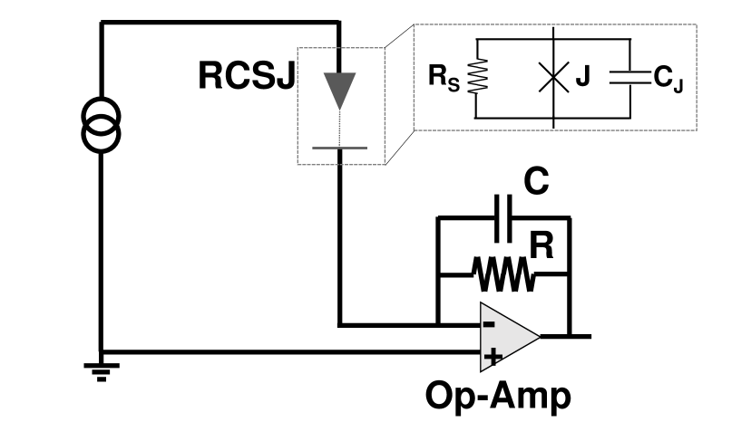
In our setup (Extended Data Figure 5), we employ a circuit featuring an operational amplifier for the feedback element, which is commonly utilized for SJS measurements [6, 7, 8, 9, 10, 11, 10, 11, 12, 13, 14, 15, 16, 17, 18, 19, 20, 21, 22, 23, 24, 25, 26, 27]. There is nevertheless an important difference between our circuit and similar ones. Typically, the resistor is chosen within the range of to M in order to prevent excessive bandwidth reduction, and an additional amplification stage is employed to achieve current-to-voltage conversions in the , or higher ranges. This amplification stage often incorporates a filter, which can eliminate any oscillatory behavior present in the junction like the bistable regime discussed in this work.
In absence of such an additional filtering stage, the current flowing through the atomic-size tunnel junction is directly measured through the operational amplifier in a current-to-voltage configuration. In our setup we use a voltage source with a 10 k resistor connected in series. The voltage drop on this resistor is subtracted from the bias voltage to obtain the curves. We determine the voltage as a function of time by multiplying the output of the operational amplifier by the tunnel resistance of the junction and subtracting an offset. The feedback of the operational amplifier ensures that the current flows through the resistor and reaches ground, thereby simultaneously nullifying the voltage difference at the amplifier’s two inputs.
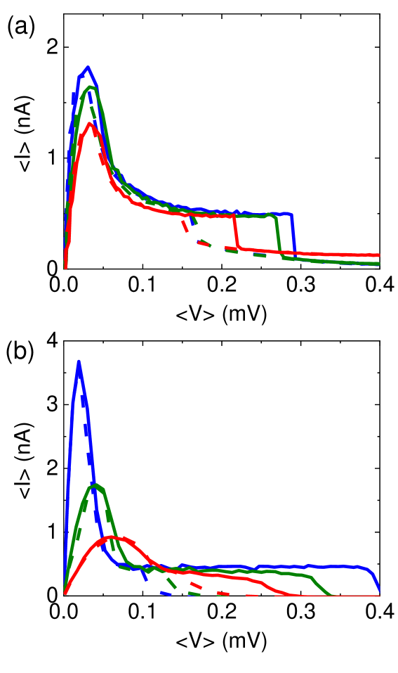
However, the feedback’s action is not immediate but rather delayed by a certain time constant , limited by the junction’s resistance and the capacitance . The capacitance in our circuit is mainly due to the capacitance in parallel to the resistor in Extended Data Figure 5, which mostly consists of the wiring to ground. This can be significant due to the typical long wiring in a dilution refrigerator setup [9, 5]. We observe the oscillatory behavior when nF. In the Al-Al experiment (discussed in the Supplementary information), we use a capacitor of nF and get an approximately ten times larger . When the setup has a capacitance of nF, further increases and the bistable regime is lost, resulting in the Josephson behavior reported in previous works, discussed in more detail in the Supplementary Information and shown in Fig.1b of the main text (blue dashed line).
In our experiment, taking , we estimate that is on the order of, or below, a few fF. The capacitance of tunnel junctions made with STM have been measured and calculated for typical tip shapes and sample-tip distances, yielding values in the range of tens of fF [28]. These capacitance values indicate that the tip can be modelled by a sphere with an effective radius somewhat below m. This suggests that the junction capacitance is primarily determined by the geometry of the tip at a distance slightly below that value, typically in the range of a few tens to hundreds of nm.
We use the OPA 111 amplifier in our setup, featuring a low bias current [29]. In the operational amplifier, two field effect transistors (FET) are connected to the input and to the power supply. The inputs ( and in Extended Data Figure 5) are connected to the gate of each FET while the power supply is connected to the source and the output to the drain of each FET. Before reaching the output, the signal is amplified through a low-noise cascode. As the gain is very large in the used circuit, we expect the settling time to be of order of the RC time of the circuit.
Acknowledgments.
Authors particularly acknowledge Juan Antonio Higuera from SEGAINVEX at UAM for the insight into the amplification circuitry used in STM. We also acknowledge discussions with Sebastián Vieira about SJS. Support by the Spanish Research State Agency (PID2020-114071RB-I00, PID2020-117671GB-100, PDC2021-121086-I00, TED2021-130546BI00 and CEX2018-000805-M), the European Research Council PNICTEYES through grant agreement 679080, grants No. PID2021-122769NB-I00 and No. PID2021-125343NB-I00 funded by MCIN/AEI/10.13039/501100011033, and by the Comunidad de Madrid through program NANOFRONTMAG-CM (S2013/MIT-2850) is acknowledged. We have benefitted from collaborations through EU program Cost CA21144 (superqumap), and from SEGAINVEX at UAM in the design and construction of STM and cryogenic equipment.
Author contributions.
Calculations were carried out by S.D.E and D.P., being supervised by E.P. and A.L.Y. The oscillatory signal was observed by V.B. and I.G. in Pb. Further experiments were carried out by J.A.M., M.F.L., M.A. and B.W., with the supervision of H.S. and I.G. The electronics, data and set-up were analyzed by J.A.H., E.H. and J.G.R. The concept was devised and the manuscript was written by S.D.E., D.P., A.L.Y. and H.S. All authors have read and approved the final manuscript.
Corresponding authors.
Correspondence to samuel.diaz-escribano@weizmann.ac.il and hermann.suderow@uam.es.
Supplementary Information
Temperature dependence of the bistable regime and results in Al and in 2H-NbSe2
We show data taken with a tip of Pb ( K) and a sample of 2H-NbSe2 ( K) in Extended Data Figure 3. 2H-NbSe2 is known to exhibit multiple superconducting gaps , which are distributed over the Fermi surface, ranging from meV to meV [30, 26, 31, 32, 33, 34, 35, 36]. This leads to the rounded bias-voltage dependence of the current-voltage characteristics above about mV shown in the upper inset of Extended Data Figure 3a. Despite these differences, the behavior regarding the bistable regime is similar to Pb-Pb junctions.
In Extended Data Figure 4, we show the results for the Al-Al junction. Due to the reduced superconducting gap compared to Pb, the voltage range is modified. Furthermore, the peak in the Josephson current is considerably reduced and the hysteresis is practically absent (Extended Data Figure 4). These curves were also taken at a relatively large temperature of 0.4 K (note that K). Nonetheless, the time-dependent oscillatory behavior in the bistable regime is still observed (Extended Data Figure 4b). We employed for these measurements a capacitor with ten times higher capacitance in the operational amplifier circuit than in the other experiments. This increased the time constant by about an order of magnitude.
Other approaches to measure the Josephson current
The current vs voltage characteristic in SJS is often understood through the phase diffusive transport approximation derived by Ivanchenko and Zilberman [37]. According to this model, the current is given by , where represents a high-frequency impedance and is a characteristic voltage. The conductance at zero bias is often used to map the Josephson current as a function of the position. However, is typically unknown [11]. Furthermore, the maximal current (for ) decreases as and the conductance at zero bias as as .
In the Fig. 1c of the main text we compare curves taken in different STM set-ups using tip and sample of Pb. We have tried to match as far as possible the conductance , which is around . In the set-up having a capacitance of around nF (blue curve) we observe the bistable regime. In the set-up having a capacitance of about nF (dashed blue curve) we observe no bistable regime. The current is then time-independent for all bias voltages and there is no hysteresis. The dashed blue curve is well captured by the Ivanchenko-Zilberman approximation.
Our model also requires an effective temperature of 1 K to obtain the shape of the curve at low bias voltages (Fig. 3c in the main text). It is important to note that the energy resolution of our experiment is far below this value, as evidenced by the sharp increase in the current at the gap edge (upper inset of Fig. 1c, and Ref. [5]). The increased temperature arises from the equivalent temperature of the electromagnetic environment at the Josephson frequency . However, we can extract the value of in the bistable regime from the oscillatory signal, which is given by and the time constants of our circuit, and is thus nearly independent of temperature for /2, following the dependence of with temperature.
Switching in and out of the bistable regime
We can analyze in more detail the effect of temperature by studying the entry and exit into and out of the bistable regime. The escape dynamics of small Josephson junctions has been extensively studied [4, 38, 39, 40, 41, 5]. The current jumps from the Josephson regime into the resistive regime with its dynamics determined by thermal activation at high temperatures and quantum tunneling at very low temperatures [4, 38].
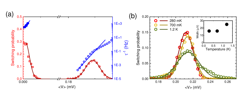
In the new bistable regime, the junction leaves the zero voltage regime and enters the bistable regime. In Extended Data Figure 6a, we show that this occurs through a stochastic process. Pulses of width are measured at time intervals that seem to be random. The inverse of the time between pulses, , increases exponentially with bias. We can find the probability of switching by taking . follows a Gaussian behavior within a range of time-averaged voltage of about (see Extended Data Figure 6a).
The junction leaves the bistable regime producing the hysteresis discussed above. To analyze this behavior, we have swept through the current-voltage characteristics many times and traced at each sweep the voltage where we lose oscillations at . From this, we define a switching probability and the corresponding time scale (Extended Data Figure 6a). As we observe in Extended Data Figure 6b, the Gaussian function that describes the switching probability becomes sharper when decreasing temperature.
Relation to relaxation oscillators and other dynamic phenomena in Josephson junctions
The nonlinear dynamics of a Josephson junction in itself, without feedback, can be extremely rich and complex, with regimes of chaotic behavior [42, 43, 44, 45, 46, 47]. Additionally, unstable regions in the current-voltage characteristics of Josephson junctions can lock into passive elements leading to an oscillatory behavior [48, 49, 50, 51, 52, 53, 54]. Often, they are called relaxation oscillators and imply the passage of the current to the dissipative regime. This is not possible in our junctions, as the voltage moves in a narrow interval close to zero, far below the superconducting gap value. Furthermore, these behaviors occur at frequencies between four and six orders of magnitude higher than those observed here [48, 49, 50, 51, 52, 53, 54].
References
- [1] Zhang Li-Sen, F. C.-W., Cai Li. Hopf bifurcation and chaotification of Josephson junction with linear delayed feedback. Acta Physica Sinica 60, 060306 (2011).
- [2] Segall, K., Schult, D., Ray, U. & Ohsumi, T. Numerical simulation of thermal noise in Josephson circuits (2016). ArxiV:1110.0172.
- [3] Rodrigo, J. G., Suderow, H., Vieira, S., Bascones, E. & Guinea, F. Superconducting nanostructures fabricated with the scanning tunnelling microscope. Journal of Physics: Condensed Matter 16, R1151 (2004).
- [4] Suderow, H., Guillamón, I. & Vieira, S. Compact very low temperature scanning tunneling microscope with mechanically driven horizontal linear positioning stage. Review of Scientific Instruments 82 (2011).
- [5] Fernández-Lomana, M. et al. Millikelvin scanning tunneling microscope at 20/22 T with a graphite enabled stick–slip approach and an energy resolution below 8 eV: Application to conductance quantization at 20 T in single atom point contacts of Al and Au and to the charge density wave of 2H–NbSe2. Review of Scientific Instruments 92, 093701 (2021).
- [6] Galvis, J. A. et al. Three axis vector magnet set-up for cryogenic scanning probe microscopy. Review of Scientific Instruments 86 (2015).
- [7] Álvarez Montoya, R. et al. Methods to simplify cooling of liquid Helium cryostats. HardwareX 5, e00058 (2019).
- [8] Horcas, I. et al. WSXM: A software for scanning probe microscopy and a tool for nanotechnology. Review of Scientific Instruments 78, 013705 (2007).
- [9] Martín-Vega, F. et al. Simplified feedback control system for scanning tunneling microscopy. Review of Scientific Instruments 92, 103705 (2021).
- [10] Šmakov, J., Martin, I. & Balatsky, A. V. Josephson scanning tunneling microscopy. Phys. Rev. B 64, 212506 (2001).
- [11] Naaman, O., Teizer, W. & Dynes, R. C. Fluctuation Dominated Josephson Tunneling with a Scanning Tunneling Microscope. Phys. Rev. Lett. 87, 097004 (2001).
- [12] Kimura, H., Barber, R. P., Ono, S., Ando, Y. & Dynes, R. C. Josephson scanning tunneling microscopy: A local and direct probe of the superconducting order parameter. Phys. Rev. B 80, 144506 (2009).
- [13] Randeria, M. T., Feldman, B. E., Drozdov, I. K. & Yazdani, A. Scanning Josephson spectroscopy on the atomic scale. Phys. Rev. B 93, 161115 (2016).
- [14] Rodrigo, J. G., Suderow, H. & Vieira, S. On the use of STM superconducting tips at very low temperatures. Eur. Phys. J. B 40, 483–488 (2004).
- [15] Pan, S. H., Hudson, E. W. & Davis, J. C. Vacuum tunneling of superconducting quasiparticles from atomically sharp scanning tunneling microscope tips. Applied Physics Letters 73, 2992–2994 (1998).
- [16] Rodrigo, J. G., Crespo, V. & Vieira, S. Josephson current at atomic scale: Tunneling and nanocontacts using a STM. Physica C 437-438, 270–273 (2006).
- [17] Guillamon, I., Suderow, H., Vieira, S. & Rodiere, P. Scanning tunneling spectroscopy with superconducting tips of Al. Physica C: Superconductivity and its Applications 468, 537 – 542 (2008).
- [18] Jäck, B. et al. Critical Josephson current in the dynamical Coulomb blockade regime. Phys. Rev. B 93, 020504 (2016).
- [19] Kohen, A. et al. Fabrication and characterization of scanning tunneling microscopy superconducting Nb tips having highly enhanced critical fields. Physica C: Superconductivity 419, 18 – 24 (2005).
- [20] Bergeal, N. et al. Mapping the superconducting condensate surrounding a vortex in superconducting V3Si using a superconducting MgB2 tip in a scanning tunneling microscope. Phys. Rev. B 78, 140507 (2008).
- [21] Proslier, T. et al. Probing the superconducting condensate on a nanometer scale. Europhysics Letters (EPL) 73, 962–968 (2006).
- [22] Edkins, S. D. et al. Magnetic field–induced pair density wave state in the cuprate vortex halo. Science 364, 976–980 (2019).
- [23] Ast, C. R. et al. Sensing the quantum limit in scanning tunnelling spectroscopy. Nature Communications 7, 13009 (2016).
- [24] Joo, S. H. et al. Cooper pair density of Bi2Sr2CaCu2O8+x in atomic scale at 4.2 K. Nano Letters 19, 1112–1117 (2019).
- [25] Chen, W. et al. Identification of a nematic pair density wave state in Bi2Sr2CaCu2O8+x. Proceedings of the National Academy of Sciences 119, e2206481119 (2022).
- [26] Liu, X., Chong, Y. X., Sharma, R. & Davis, J. C. S. Atomic-scale visualization of electronic fluid flow. Nature Materials 20, 1480–1484 (2021).
- [27] Steiner, J. F., Melischek, L., Trahms, M., Franke, K. J. & von Oppen, F. Diode effects in current-biased josephson junctions. Phys. Rev. Lett. 130, 177002 (2023).
- [28] de Voogd, J. et al. Fast and reliable pre-approach for scanning probe microscopes based on tip-sample capacitance. Ultramicroscopy 181, 61–69 (2017).
- [29] Burr-Brown. Low noise precision operational amplifier OPA111 Datasheet.
- [30] Guillamón, I., Suderow, H., Guinea, F. & Vieira, S. Intrinsic atomic-scale modulations of the superconducting gap of 2H-NbSe2. Phys. Rev. B 77, 134505 (2008).
- [31] Sanna, A. et al. Real-space anisotropy of the superconducting gap in the charge-density wave material 2H-NbSe2. npj Quantum Materials 7, 6 (2022).
- [32] Yokoya, T. et al. Fermi surface sheet-dependent superconductivity in 2H-NbSe2. Science 294, 2518–2520 (2001).
- [33] Noat, Y. et al. Quasiparticle spectra of 2H-NbSe2: Two-band superconductivity and the role of tunneling selectivity. Phys. Rev. B 92, 134510 (2015).
- [34] Huang, C. L. et al. Experimental evidence for a two-gap structure of superconducting 2H-NbSe2: A specific-heat study in external magnetic fields. Phys. Rev. B 76, 212504 (2007).
- [35] Boaknin, E. et al. Heat conduction in the vortex state of 2H-NbSe2: Evidence for multiband superconductivity. Phys. Rev. Lett. 90, 117003 (2003).
- [36] Rodrigo, J. G. & Vieira, S. STM study of multiband superconductivity in NbSe2 using a superconducting tip. Physica C: Superconductivity 404, 306–310 (2004). Proceedings of the Third European Conference on Vortex Matter in Superconductors at Extreme Scales and Conditions.
- [37] Ivanchenko, Y. M. & Zil’berman, L. The Josephson effect in small tunnel contacts. JETP 28, 1272 (1969).
- [38] Devoret, M. H., Martinis, J. M. & Clarke, J. Measurements of macroscopic quantum tunneling out of the zero-voltage state of a current-biased Josephson junction. Phys. Rev. Lett. 55, 1908–1911 (1985).
- [39] Massarotti, D. et al. Escape dynamics in moderately damped Josephson junctions (Review Article). Low Temperature Physics 38, 263–272 (2012).
- [40] Tafuri, F. Fundamentals and frontiers of the Josephson effect, vol. 286 of Springer Series in Materials Science (Springer, Switzerland, 2019).
- [41] Longobardi, L. et al. Direct transition from quantum escape to a phase diffusion regime in YBaCuO biepitaxial Josephson junctions. Phys. Rev. Lett. 109, 050601 (2012).
- [42] Whan, C. B. & Lobb, C. J. Complex dynamical behavior in RCL-shunted Josephson tunnel junctions. Phys. Rev. E 53, 405–413 (1996).
- [43] Cawthorne, A. B., Whan, C. B. & Lobb, C. J. Complex dynamics of resistively and inductively shunted Josephson junctions. Journal of Applied Physics 84, 1126–1132 (1998).
- [44] Miracky, R. F., Devoret, M. H. & Clarke, J. Deterministic hopping in a Josephson circuit described by a one-dimensional mapping. Phys. Rev. A 31, 2509–2519 (1985).
- [45] Meister, S. et al. Resonators coupled to voltage-biased Josephson junctions: From linear response to strongly driven nonlinear oscillations. Phys. Rev. B 92, 174532 (2015).
- [46] Dalla Torre, E. G., Demler, E., Giamarchi, T. & Altman, E. Dynamics and universality in noise-driven dissipative systems. Phys. Rev. B 85, 184302 (2012).
- [47] Kleiner, R. et al. Space-time crystalline order of a high-critical-temperature superconductor with intrinsic Josephson junctions. Nature Communications 12, 6038 (2021).
- [48] Muck, M. & Heiden, C. Simple DC-SQUID system based on a frequency modulated relaxation oscillator. IEEE Transactions on Magnetics 25, 1151–1153 (1989).
- [49] Fulton, T. A. Relaxation oscillation logic in Josephson junction circuits (U.S. Patent No. 4 249 094A, Dec 1978).
- [50] Dechert, J., Krischker, K., Goddenhenrich, T., Muck, M. & Heiden, C. Self-oscillating micro-SQUIDs for application in a scanning SQUID microscope. IEEE Transactions on Applied Superconductivity 7, 3143–3146 (1997).
- [51] Onomi, T. Experimental demonstration and performance estimation of a new relaxation oscillator using a superconducting Schmitt trigger inverter. Physics Procedia 81, 141 – 144 (2016). Proceedings of the 28th International Symposium on Superconductivity (ISS 2015) November 16-18, 2015, Tokyo, Japan.
- [52] Taur, Y. & Richards, P. L. Relaxation oscillations in point-contact Josephson junctions. Journal of Applied Physics 46, 1793–1797 (1975).
- [53] Mück, M., Rogalla, H. & Heiden, C. Relaxation oscillators made of bridge-type Josephson contacts. Applied Physics A 46, 97–101 (1988).
- [54] Calander, N., Claeson, T. & Rudner, S. A subharmonic Josephson relaxation oscillator-amplification and locking. Applied Physics Letters 39, 504–506 (1981).