Design Automation for Silicon Dangling Bond Logic under Atomic Defects on the H-Si(100)-2×1 Surface
A Physical Design Flow for Silicon Dangling Bond Logic under Atomic Defects on the H-Si(100)-2×1 Surface
Defect-Aware Physical Design of Silicon Dangling Bond Logic
Atomic Defect-Aware Physical Design of
Silicon Dangling Bond Logic on the H-Si(100)-2×1 Surface
Abstract
Although fabrication capabilities of Silicon Dangling Bonds have rapidly advanced from manual labor-driven laboratory work to automated manufacturing in just recent years, sub-nanometer substrate defects still pose a hindrance to production due to the need for atomic precision. In essence, unpassivated or missing surface atoms, contaminants, and structural deformations disturb the fabricated logic or prevent its realization altogether. Moreover, design automation techniques in this domain have not yet adopted any defect-aware behavior to circumvent the present obstacles. In this paper, we derive a surface defect model for design automation from experimentally verified defect types that we apply to identify sensitivities in an established gate library in an effort to generate more robust designs. Furthermore, we present an automatic placement and routing algorithm that considers scanning tunneling microscope data obtained from physical experiments to lay out dot-accurate circuitry that is resilient against the presence of atomic surface defects. This culminates in a holistic evaluation on surface data of varying defect rates that enables us to quantify the severity of such defects. We project that fabrication capabilities must achieve defect rates of around , if charged defects can be completely eliminated, or , otherwise. This realization sets the pace for future efforts to scale up this promising circuit technology.
I Introduction & Motivation
With the decline of Moore’s Law, research has turned to alternative circuit technologies in the search for promising post-CMOS candidates. A relatively new contestant in this domain are Silicon Dangling Bonds (SiDBs) that act as atomically-sized quantum dots and that have seen tremendous fabrication advancements in the recent years [1, 2, 3, 4, 5, 6, 7]. Under the term atomic silicon quantum dots, their application for the creation of nanometer-sized logic cells has been investigated which led to the successful demonstration of a sub- SiDB OR gate and wire segments on hydrogen-passivated silicon surfaces [8]. Relying on Coulomb interaction instead of the transmission of electric current, SiDB logic implements the Field-coupled Nanocomputing (FCN) paradigm [9] that offers logic-in-memory devices [10, 11] and promises energy dissipation capabilities below the Landauer limit [12, 13, 14, 10, 15], or clock frequencies in the terahertz regime [16, 17, 18, 19, 20].
Motivated by this, the research community has already taken interest in the SiDB platform for logic design; an effort that resulted in the creation of various physical simulators [21, 19, 18, 22, 23, 24], various manually designed circuits and some gate libraries [21, 18, 20, 25, 26, 27, 28, 29], as well as algorithms for placement and routing of SiDB gates [28, 30].
However, SiDB fabrication requires atomic precision and, thus, is prone to substrate defects at the sub-nanometer level. These defects naturally occur during the substrate preparation, i. e., in the process of preparing a pure hydrogen-passivated silicon (H-Si(100)-2×1) surface for SiDB fabrication. They are generally classified as any atomic structure that does not follow the H-Si(100)-2×1 surface reconstruction, in which each surface silicon atom is bonded to a neighboring silicon atom creating a dimer pair, a hydrogen atom from the passivation, and two silicon atoms in the bulk of the crystal [31]. Such defects could include unpassivated surface silicon atoms, missing silicon atoms, contaminant atoms, or structural deformations (which is covered in more detail in Section III).
Current fabrication of SiDB logic necessitates the scanning for defect-free regions that are large enough to host the intended layout on the substrate at hand [32]. While being a useful proof-of-concept demonstration, this fabrication approach is not only wasteful, but also increasingly unrealistic with growing layout size as it can accommodate for a handful of gates at the utmost. Hence, the presence of surface defects imposes a hindrance on scaling SiDB design size. At the same time, operating at the atomic-scale, material defects are largely common at the current fabrication capabilities.
Accordingly, the electrostatic effects of such surface defects have been closely examined—providing insights into how they might limit SiDB fabrication and the operation of fabricated SiDB devices [33, 34]. This work leverages these defect analysis findings to enable automatic layout design under the presence of atomic surface defects.
In this regard, the paper at hand proposes the following contributions:
-
1.
the derivation of an atomic defect model by the establishment of equivalence classes among 13 experimentally verified H-Si(100)-2×1 defect types to guide design automation methodologies,
-
2.
a case study of applying said defect model to the established Bestagon gate library [28], which led to the identification of sensitivities of some gates to certain defects for which we propose more robust redesigns,
-
3.
an automatic placement and routing algorithm that considers real Scanning Tunneling Microscope (STM) surface scans obtained from physical experiments as well as simulated surface data to design functioning dot-accurate SiDB circuit layouts in the presence of atomic surface defects by avoiding disturbed regions, and
-
4.
a culmination of the previously mentioned contributions into a holistic experimental evaluation on H-Si(100)-2×1 surfaces of variable defect rates that quantifies the severeness of—particularly—charged atomic defects.
Thereby, we propose the first defect-aware framework for SiDB logic that amalgamates fabrication and design automation. Experimental evaluations on both real and simulated H-Si(100)-2×1 surfaces allow us to estimate the required surface manufacturing quality in terms of the defect rate for large-scale SiDB device fabrication in future efforts to be around , if charged defects can be completely eliminated or , otherwise.
The remainder of this manuscript is structured as follows: in an effort to establish this paper as a stand-alone work, Section II reviews related material on SiDB fabrication and their logic platform to constitute the foundation upon which this paper is built. Afterward, Section III introduces atomic defects on the H-Si(100)-2×1 surface and discusses their effects on SiDB systems. Based on that, Section IV presents the proposed defect-aware physical design methodology by first establishing a surface defect model and, then, discussing algorithmic details. An experimental evaluation of the approach is conducted in Section V. Finally, Section VI concludes the paper and gives an outlook on future work in the domain.
II Silicon Dangling Bond Logic
As an implementation of the FCN paradigm [9], the utilization of SiDBs has recently gained momentum. Using an atomically-sharp tip of a Scanning Tunneling Microscope (STM), individual dangling bonds can be created on a hydrogen-passivated silicon surface at the single-atom scale [3, 2, 4, 35, 36, 37, 38, 39]. These dangling bonds act as quantum dots and are used to represent logic states and to realize Boolean operations at the limit of physical scaling [1, 8, 5, 40, 41].
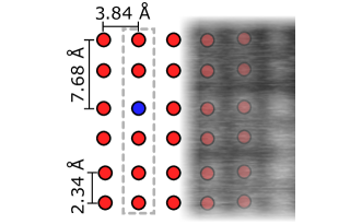
The most commonly used surface phase for SiDB creation is H-Si(100)-2×1 whose atomic structure is illustrated in Fig. 1. The surface consists of discretely defined sites (shown as red atoms in Fig. 1d), where SiDBs can be fabricated with atomic precision. By using the scanning probe tip to inject current into the H-Si bond, it is possible to selectively remove single hydrogen atoms from the surface, leaving behind an SiDB (shown in blue in Fig. 1b–1d).
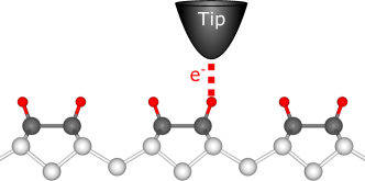
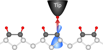
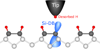
The resulting SiDBs may possess 0, 1, or 2 electrons, corresponding to positive, neutral, and negative charge states, respectively.111Note that, in the following only negative or neutral dangling bonds are of interest. Positively charged ones are not relevant for gate configurations [21, 8] The corresponding charge states can be controlled by environmental factors such as the bulk dopant concentration [42] and the presence of electric fields [40, 36]. A groundbreaking demonstration by Huff et al. has experimentally demonstrated that careful configurations of pairs of SiDBs can be used to realize logic components [8]. These SiDB pairs are observed to share a single additional electron between them which can be manipulated to occupy the left or right SiDB of the pair indicating a binary 0 or 1 state; a behavior that was coined Binary-Dot Logic (BDL) [8].
These electronic properties enable the realization of BDL wire structures as well as a sub logic OR gate [8]. A simulated reproduction of the OR gate using the SiDB simulator SiQAD [21] is shown in Fig. 2. Here, the input bit states are set by the addition of a peripheral SiDB, dubbed a perturber [8, 21], which exerts an external field on the input SiDB pair to emulate the presence of an input BDL wire at the logic state. When one or both of the input SiDB pairs are set to logic by input perturbers, the output also toggles to logic as expected of an OR gate. It is to be noted that the need for these perturbers will be alleviated upon the future development of I/O devices.
The recent physical accomplishments and the upcoming commercialization [43, 44] in the domain of SiDB logic have triggered an increasing interests in design automation methods for this technology—yielding first CAD tools, circuit layouts, and physical design algorithms [21, 19, 18, 22, 23, 24, 20, 25, 26, 27, 28, 29, 30]. However, none of these methodologies and proposals take into account that the fabrication of sub-nanometer structures is naturally error-prone and that atomic defects of the substrate are inherent to this endeavor and will continue to be for the foreseeable future [33, 34]. The following section covers common atomic defects on the H-Si(100)-2×1 surface and their influence on SiDB logic.
III Atomic Surface Defects
Despite the relative cleanliness of H-Si(100)-2×1 compared to other crystal faces of silicon [31], there still exists a natural concentration of defects that cannot be completely avoided with current in-situ preparation methods. These defects can be broadly described as any collection of atoms in the crystal that do not form the 21 surface phase, where each surface silicon atom is host to only one hydrogen. These could include unpassivated surface silicon atoms, missing silicon atoms, contaminant atoms, or structural deformations. To this end, defects prevent the creation of atomically identical SiDBs due to their varying structures. Additionally, the proximity of defects alters SiDB behavior and, consequently, corrupts implemented logic gates.
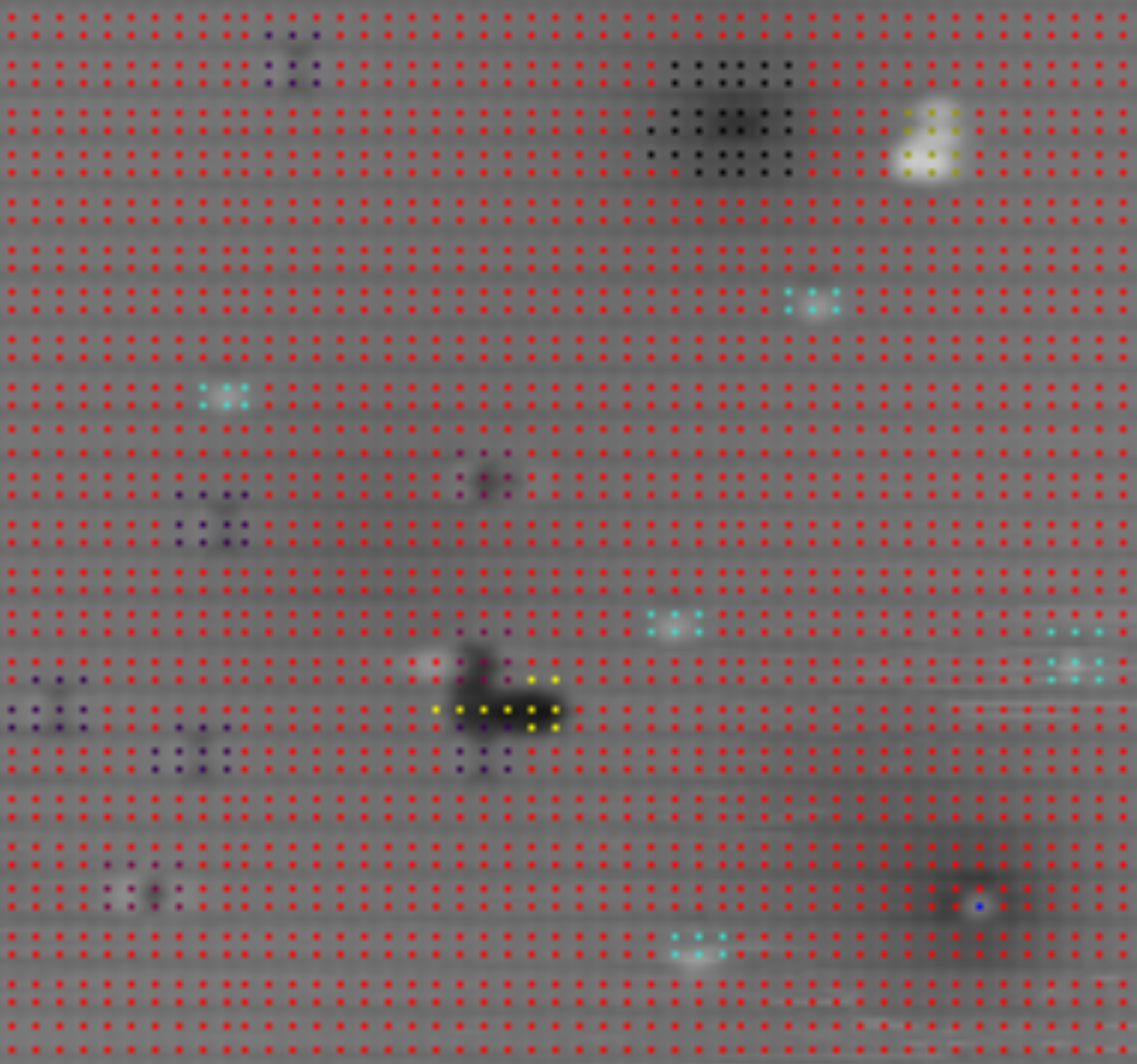
As an example, Fig. 3a depicts an empty states STM scan acquired at and of a physically fabricated H-Si(100)-2×1 surface. The black frames with alphabetical labels indicate different atomic defects. Fig. 3b to Fig. 3g illustrate these defects as a side-view ball-and-stick model. The following list gives a brief explanation of their nature:222A more detailed discussion of these and other commonly occurring defects can be found in [33].
-
3b
The defect-free H-Si(100)-2×1 surface phase. Each surface silicon atom in dark gray is paired with another surface silicon atom creating a dimer pair. Each silicon atom of a dimer is then passivated with a single hydrogen atom. Each silicon atom in this configuration is capable of hosting a single, chemically identical dangling bond.
-
3c
A silicon atom that is not terminated with hydrogen leaving a dangling bond. These can be intentionally created, or found from incomplete hydrogen passivation.
-
3d
A dihydride pair, where no dimer bond forms, leaving each silicon atom to bond with two hydrogen atoms. Dihydrides are found more often when the crystal annealing temperature is too low [45].
-
3e
A silicon vacancy, where a single silicon atom is missing from the lattice leaving unsatisfied subsurface dangling bonds.
-
3f
A siloxane dimer, which features a single oxygen atom between the two silicon atoms of the dimer. This defect occurs in high concentration when the preparation chamber is contaminated with water molecules.
-
3g
A missing dimer where both silicon atoms are absent.
Atomic defects can furthermore also appear in various combinations on the same or adjacent dimers which increases their affects on logic placed in their vicinity [33].
To the best of the authors’ knowledge, no related work on SiDB logic and design automation has considered the impact atomic defects have on their proposed layouts. This disregard of physical effects leaves most approaches conflicting with existing fabrication capabilities.
In the following section, we are addressing this shortcoming by proposing a physical design methodology that is aware of atomic defects. Consequently, the layouts automatically generated by the proposed approach avoid defective surface positions.
IV Defect-Aware Physical Design
In this section, we introduce a solution that addresses the shortcomings of existing physical design methods for SiDB logic discussed above. To this end, we first propose an abstract surface defect model for automatic design that is based on the physical properties of the identified atomic surface defects. Afterward, we propose a defect-aware physical design method that, utilizing the proposed model, is able to realize SiDB logic that behaves as intended on an otherwise defective surface.
IV-A Surface Defect Model
Before being able to apply any defect-aware design methodology, the atomic structure of the specific surface at hand must be analyzed and defects identified. In this instance, defects are autonomously classified using a Convolutional Neural Network (CNN) similar to that developed in [32]. Its input is an STM image like that in Fig. 3a. The CNN provides a pixel-based classification of the surface corresponding to the defect types as its output. The classification is then correlated to the lattice positions of the H-Si(100)-2×1 surface yielding a coordinate-based defect assignment as shown in Fig. 4. Hydrogen-terminated silicon (defect-free dimers) is labeled in red, while various defects are labeled as described in the caption.333Looking at the defect lattice positions, one can see that some assigned labels extend farther than the underlying physical defect. This is due to the output of the CNN. When labeling the training data, defects were marked based on their contrast in the acquired images and not the exact lattice coordinates. Since some defects had a strong influence on the contrast of adjacent, defect-free atoms, they were labeled as the same defect to avoid any aliasing in defect classification. It is possible to apply a filter as a post-processing step to limit each defect label to its exact atomic position as shown for the dangling bond defect (in blue) near the bottom-right corner of Fig. 4. Since it is necessary to keep some distance from the various defects anyway, such filtering is not a crucial step of the proposed methodology. However, localizing stray dangling bond defects with atomic accuracy can be beneficial in another way: if they happen to coincide with SiDB positions of placed gates, they can be seamlessly integrated rather than considering them as defects that must be avoided.
Once each lattice position has been classified, the atomic defects of the H-Si(100)-2×1 surface can be further divided into two categories: charged and uncharged (neutral). The overall charge of a defect is dependent on both the atomic structure and the crystal doping level. Since the crystals considered in this work are degenerately n-doped, all electron energy levels within the band gap are filled resulting in negatively charged defects.
These residual negative charges (as observed in dangling bond and silicon vacancy defects) are able to exert screened Coulombic effects on the charge state of nearby SiDBs as demonstrated by experiments in the literature [34]. Different gates may have a varying tolerance against these effects, which can be found by running fixed charge defect simulations for defect types of interest using SiQAD [21, 46]. The physical parameters of silicon vacancy defects have been fitted in [34] and recreated in simulation in [46]. With these resources, we have developed the following procedure to determine the minimum distance that each gate tile of a given library must avoid a defect by in order to achieve correct logic operation for that tile in isolation:
-
1.
Place the defect at distance from the gate.
-
2.
Run physical simulations of the gate toggling through all possible input signal combinations.
-
3.
For each simulation run, check that the input and output SiDB pairs hold the correct binary logic state.
-
4.
If any input combination results in incorrect logic states, return as the minimum avoidance distance.
-
5.
Repeat for a sufficient count of defect locations and values of to cover meaningful distances in the vicinity of the gate.
We have applied this procedure to the Bestagon gate library [28] with silicon vacancy defects placed at spacings in both and directions, under the surface within a grid centered on each gate. We have found that some Bestagon tiles are not functional at any tested defect distance, necessitating the redesign of these nonfunctional logic tiles. We have, therefore, redesigned them using an automated SiDB layout designer based on reinforcement learning [47] and selected candidates that have the lowest minimum avoidance distances. The global minimum avoidance distance was found to be by taking the worst performing minimum avoidance distance out of all tiles. A repository is made publicly available on GitHub444https://github.com/cda-tum/sidb-defect-aware-physical-design containing 1. SiQADdesign files of the redesigned tiles, 2. evaluation results for minimum avoidance distance of these tiles, 3. the original Bestagon tiles, and 4. a list of nonfunctional tiles that do not have a proposed direct replacement. The latter applies foremost to the half-adder tile which can however be decomposed into, e. g., an XOR and an AND tile.
IV-B Automatic Physical Design
The de-facto standard for physical design in the FCN domain is that of a tile-based abstraction [48, 49, 50, 51, 52, 53]. That is, a (uniform) tiling of a surface is provided where each tile can implement one designated Boolean function. A standard library of pre-designed SiDB gates and wire segments can be applied to generate a dot-accurate layout from such a gate-level abstraction. Thereby, the focus is shifted from the physical to the logic level and, thus, assists placement and routing by limiting the search space [54, 51, 52, 53]. Additionally, logic-level simulation and verification are enabled [55].
Surface tilings come in manifold forms with the most common one being the Cartesian grid where each tile is a rectangle [48, 49, 56, 57]. Recently, hexagonal tilings were established for SiDBs [28], because they intrinsically match the Y-shaped SiDB gates that have been experimentally proven by Huff et al. [8], and as such provide a more realistic abstraction for SiDB circuit layouts.
This work, thus, also relies on tile-based design. In the following, we assume a hexagonal tiling together with established SiDB gates [28]. However, our approach is generic such that any tiling and any standard library can be applied.
Instead of imagining a perfect, idealized surface, we consider a realistic STM surface scan as input to our algorithm. We overlay a tiling and match each gate and wire of a given gate library in every rotation against each tile and analyze the effects of defects in the proximity of each dot that make up the gate/wire tile. This procedure yields a blacklist of gate-tile pairs, i. e., a listing of SiDB structures that cannot operate properly on certain tiles of the surface.
We pass this blacklist as a set of placement and routing constraints to a satisfiability-based algorithm that avoids placing those gates/wires on the specified tiles in the specified rotation. The result is a dot-accurate layout that avoids all defects on the surface and, thus, preserves functionality in the presence of disturbances.
Benchmark [28] Examined Surface Data Experimental STM Scans Simulated w/ Charged Defects Simulated w/o Charged Defects defect-free defective defective defective defective defective defective defective defective Name #SiDBs A[] #SiDBs A[] #SiDBs A[] #SiDBs A[] #SiDBs A[] #SiDBs A[] #SiDBs A[] #SiDBs A[] #SiDBs A[] xor2 — — — — xnor2 — — — — par_gen — — — — — — mux21 — — — — — — — — — — par_check — — — — — — — — — — xor5_r1 — — — — — — — — xor5_majority — — — — — — t — — — — — — — — — — t_5 — — — — — — — — — — c17 — — — — — — — — — — majority — — — — — — — — — — — — majority_5_r1 — — — — — — — — — — — — cm82a_5 — — — — — — — — — — — — — — newtag — — — — — — — — — — — —
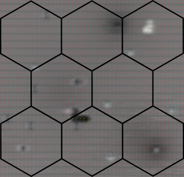
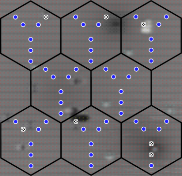
The following example shall illustrate this process. Assume the STM surface scan depicted in Fig. 3 was to be used as input to the proposed defect-aware physical design algorithm together with Huff et al.’s SiDB OR gate [8] as the target technology. The detected defects are to be avoided while employing a tile-based design paradigm for abstraction and search space restriction. Fig. 5a shows a hexagonal tiling laid over said STM surface scan from Fig. 3. Note that the size and rotation of the hexagons depend on the applied standard library.
In Fig. 5b, Huff et al.’s OR gate is matched against each tile and the effects of present defects on each SiDB are analyzed. The SiDBs indicated with a crosed-out black dot conflict with surface defects. Any gate that has at least one conflicting SiDB is excluded from being placed on that particular tile in that particular rotation. The same is repeated for all rotations of all gates/wires in the given standard library. This procedure yields the aforementioned placement blacklist.
For any given circuit specification, the resulting placement and routing problem with the blacklist is encoded as a satisfiability instance as successfully demonstrated in [51, 52]. A satisfying solution to the instance yields a conflict-free placement and routing on the surface. Due to the search space restrictions that have been employed by relying on tile-based design, it cannot be guaranteed that no such solution exists if the satisfiability instance returns UNSAT. However, the specification can be resynthesized and/or the tile overlay shifted across the surface in order to attempt finding a satisfying solution.
V Experimental Evaluations
In this section, we present and discuss the results of an experimental evaluation of the proposed defect-aware physical design approach. To this end, we applied the algorithm to automatically generate SiDB layouts on defective H-Si(100)-2×1 surfaces, both real and simulated. The following Section V-A goes over our experimental setups while Section V-B discusses the results and their implications.
V-A Experimental Setups
V-A1 Fabrication
Of the surfaces used in this evaluation, two were experimentally fabricated in a lab and measured with an STM, the others were simulated based on experimental findings.
The STM measurements were performed using an Omicron LT-STM system operating at and ultra-high vacuum (). The STM tips were electrochemically etched from tungsten wire and sharpened using a field ion microscope [58]. The used samples are highly arsenic-doped (). They were prepared in-situ via resistive heating. To this end, they were first degassed at overnight followed by multiple flash annealing cycles at . Finally, the samples were hydrogen-terminated at while exposing their surface to molecular hydrogen (). The H2 gas was converted to atomic hydrogen using a tungsten filament held at .
The image acquisition was done using a Nanonis SPM controller with respective software. All images were taken in constant height mode with an imaging bias of and a current setpoint of .
V-A2 Programming
The architecture and training of the neural network used for defect identification in STM scans is modeled after [32] and implemented in Python using Keras with the TensorFlow backend. As an addition, the training data was expanded by a factor of three and the number of classes increased to a total of 13 different defect types. The proposed defect-aware physical design algorithm was implemented in C++17 on top of the fiction framework [59] as part of the Munich Nanotech Toolkit (MNT).555Publicly available at https://github.com/cda-tum/fiction. The utilized SMT solver is Z3 [60]. All experiments were compared against the state-of-the-art results for defect-free SiDB layouts presented in [28]. The obtained layouts were formally verified for logical correctness using the approach presented in [55]. All evaluations were run on a Manjaro 23 machine with an AMD Ryzen 7 PRO 5850U CPU with 1.90 GHz (up to 4.40 GHz boost) and 32 GB of DDR4 main memory.
V-B Results
The STM scans of the fabricated H-Si(100)-2×1 surfaces span a total of and hydrogen sites, respectively, of which and are defective.666Not counting stray DB defects, as they can be erased from the surface prior to the fabrication of circuitry [2]. We applied the proposed atomic defect-aware physical design algorithm to generate the same set of benchmark circuits used in [28] while obeying the presented surface defect model, and using the Bestagon gates that we redesigned for defect robustness.
The results for these cases are listed in Table I under the caption Experimental STM Scans. For all evaluations, we list the number of required SiDBs to implement each circuit and its bounding box area in . As can be seen, not a single layout could be successfully generated—as is indicated by the dashes—due to the relatively high defect rates of the fabricated samples—highlighting the critical severity of atomic defects in logic design.
To this end, we strive for quantifying their impact by evaluating simulated surfaces of comparable size with variable defect rates of , , and , once with both charged and neutral atomic defects, and once with only neutral defects, using the same benchmark set. The obtained results can be found in the same table under the caption Simulated w/ Charged Defects for surfaces including charged defects, and under Simulated w/o Charged Defects for surfaces with purely neutral defects. In both cases, defect types were automatically distributed in accordance with experimental findings. In the former case, charged ones make up of all defects.
Three core findings can be obtained from these results: 1. defect avoidance directly correlates with significantly larger overall area consumption, 2. high defect rates, and particularly charged defects, have a tremendous impact on layout generation to the degree where circuits cannot be realized in their vicinity at all, and 3. fabrication capabilities must achieve a defect rate of around in the absence of charged defects or with charged defects present to enable sophisticated layout manufacturing.
VI Conclusions
Fabrication capabilities of Silicon Dangling Bonds (SiDBs) have advanced to the automated manufacturing stage. Nevertheless, atomic substrate defects are currently preventing technology scaling as they disturb gate functionalities or prevent logic realization altogether. In this work, we presented a surface defect model to guide physical design that we obtained by investigating 13 experimentally verified H-Si(100)-2×1 defect types. Furthermore, we proposed modifications to an established SiDB gate library to increase its robustness against substrate defects. Finally, we proposed a defect-aware placement and routing algorithm that considers STM surface scans obtained from experimentation as well as simulated surface data and designs functioning SiDB circuit layouts in the presence of atomic defects. An experimental evaluation on real fabricated surfaces demonstrated its functioning but also highlighted the limitations of current fabrication capabilities. We demonstrated the critical impact that charged defects have on the creation of circuit layouts and determined a defect rate of around , if charged defects can be completely eliminated, or , otherwise, to be required for the future of large-scale SiDB logic manufacturing. Herewith, this work represents an amalgamation of fabrication and design automation that provides the basis for large-scale defect-aware physical design of SiDB circuitry.
References
- [1] M. B. Haider et al., “Controlled Coupling and Occupation of Silicon Atomic Quantum Dots at Room Temperature,” Physical Review Letters, vol. 102, no. 4, p. 046805, 2009.
- [2] T. R. Huff et al., “Atomic White-Out: Enabling Atomic Circuitry through Mechanically Induced Bonding of Single Hydrogen Atoms to a Silicon Surface,” ACS Nano, vol. 11, no. 9, pp. 8636–8642, Sep. 2017.
- [3] N. Pavlic̆ek et al., “Tip-induced Passivation of Dangling Bonds on Hydrogenated Si(100)-21,” Applied Physics Letters, vol. 111, no. 5, p. 053104, 2017.
- [4] R. Achal et al., “Lithography for Robust and Editable Atomic-Scale Silicon Devices and Memories,” Nature Communications, vol. 9, no. 1, p. 2778, Jul. 2018.
- [5] R. A. Wolkow et al., Silicon Atomic Quantum Dots Enable Beyond-CMOS Electronics. Springer, 2014, pp. 33–58.
- [6] J. Croshaw et al., “Ionic Charge Distributions in Silicon Atomic Surface Wires,” Nanoscale, vol. 13, pp. 3237–3245, 2021. [Online]. Available: http://dx.doi.org/10.1039/D0NR08295C
- [7] J. Wyrick et al., “Atom-by-Atom Fabrication of Single and Few Dopant Quantum Devices,” Advanced Functional Materials, vol. 29, p. 1903475, 2019.
- [8] T. Huff et al., “Binary Atomic Silicon Logic,” Nature Electronics, vol. 1, pp. 636–643, 2018.
- [9] N. G. Anderson et al., Field-coupled Nanocomputing: Paradigms, Progress, and Perspectives. New York: Springer, 2014.
- [10] J. Jiao et al., “Building Blocks for the Molecular Expression of Quantum Cellular Automata. Isolation and Characterization of a Covalently Bonded Square Array of Two Ferrocenium and Two Ferrocene Complexes,” Journal of the American Chemical Society, vol. 125, no. 25, pp. 7522–7523, 2003.
- [11] H. Qi et al., “Molecular Quantum Cellular Automata Cells. Electric Field Driven Switching of a Silicon Surface Bound Array of Vertically Oriented Two-Dot Molecular Quantum Cellular Automata,” Journal of the American Chemical Society, vol. 125, no. 49, pp. 15 250–15 259, 2003.
- [12] R. Landauer, “Irreversibility and Heat Generation in the Computing Process,” IBM Journal of Research and Development, vol. 5, no. 3, pp. 183–191, 1961.
- [13] R. W. Keyes et al., “Minimal Energy Dissipation in Logic,” IBM Journal of Research and Development, vol. 14, no. 2, pp. 152–157, 1970.
- [14] C. S. Lent et al., “Bennett clocking of quantum-dot cellular automata and the limits to binary logic scaling,” Nanotechnology, vol. 17, no. 16, pp. 4240–4251, 2006.
- [15] G. Toth et al., “Quasiadiabatic switching for metal-island quantum-dot cellular automata,” Journal of Applied Physics, vol. 85, no. 5, pp. 2977–2984, 1999.
- [16] J. Timler et al., “Power Gain and Dissipation in Quantum-dot Cellular Automata,” Journal of Applied Physics, vol. 91, no. 2, pp. 823–831, 2002.
- [17] L. Livadaru et al., “Dangling-bond Charge Qubit on a Silicon Surface,” New Journal of Physics, vol. 12, no. 8, p. 083018, Aug. 2010.
- [18] S. S. H. Ng, “Computer-aided Design of Atomic Silicon Quantum Dots and Computational Applications,” Master’s thesis, University of British Columbia, 2020.
- [19] H. N. Chiu et al., “PoisSolver: A Tool for Modelling Silicon Dangling Bond Clocking Networks,” in IEEE-NANO. Montreal, QC, Canada: IEEE, Jul. 2020, pp. 134–139.
- [20] H. N. Chiu, “Simulation and Analysis of Clocking and Control for Field-coupled Quantum-dot Nanostructures,” Master’s thesis, University of British Columbia, 2020.
- [21] S. S. H. Ng et al., “SiQAD: A Design and Simulation Tool for Atomic Silicon Quantum Dot Circuits,” TNANO, vol. 19, pp. 137–146, 2020.
- [22] J. Drewniok et al., “QuickSim: Efficient and Accurate Physical Simulation of Silicon Dangling Bond Logic,” in IEEE-NANO, 2023, pp. 817–822.
- [23] ——, “Temperature Behavior of Silicon Dangling Bond Logic,” in IEEE-NANO, 2023, pp. 925–930.
- [24] ——, “The need for speed: Efficient exact simulation of silicon dangling bond logic,” 2023.
- [25] A. N. Bahar et al., “Atomic Silicon Quantum Dot: A New Designing Paradigm of an Atomic Logic Circuit,” TNANO, pp. 807–810, 2020.
- [26] M. D. Vieira et al., “Novel Three-Input Gates for Silicon Quantum Dot,” in SBCCI, 2021, pp. 1–6.
- [27] ——, “Three-Input NPN Class Gate Library for Atomic Silicon Quantum Dots,” IEEE Design & Test, 2022.
- [28] M. Walter et al., “Hexagons are the Bestagons: Design Automation for Silicon Dangling Bond Logic,” in DAC, vol. 22, 2022.
- [29] S. S. H. Ng et al., “A Blueprint for Machine Learning Accelerators Using Silicon Dangling Bonds,” in IEEE-NANO, 2023.
- [30] S. Hofmann et al., “Scalable Physical Design for Silicon Dangling Bond Logic: How a 45° Turn Prevents the Reinvention of the Wheel,” in IEEE-NANO, 2023, pp. 872–877.
- [31] J. J. Boland, “Scanning tunnelling microscopy of the interaction of hydrogen with silicon surfaces,” Advances in Physics, vol. 42, no. 2, pp. 129–171, 1993.
- [32] M. Rashidi et al., “Deep learning-guided surface characterization for autonomous hydrogen lithography,” Machine Learning: Science and Technology, vol. 1, no. 2, 2020.
- [33] J. Croshaw et al., “Atomic defect classification of the H-Si(100) surface through multi-mode scanning probe microscopy,” Beilstein Journal of Nanotechnology, vol. 11, no. 1, pp. 1346–1360, 2020.
- [34] T. Huff et al., “Electrostatic Landscape of a Hydrogen-Terminated Silicon Surface Probed by a Moveable Quantum Dot,” ACS Nano, vol. 13, no. 9, pp. 10 566–10 575, 2019.
- [35] M. Rashidi et al., “Automated Atomic Scale Fabrication,” US Patent 20 220 130 033, 2022.
- [36] T. Huff et al., “Electrostatic Landscape of a Hydrogen-Terminated Silicon Surface Probed by a Moveable Quantum Dot,” ACS Nano, vol. 13, no. 9, pp. 10 566–10 575, 2019.
- [37] R. Achal et al., “Detecting and Directing Single Molecule Binding Events on H-Si (100) with Application to Ultradense Data Storage,” ACS Nano, vol. 14, no. 3, pp. 2947–2955, 2019.
- [38] J. Onoda et al., “Ohmic Contact to Two-Dimensional Nanofabricated Silicon Structures with a Two-Probe Scanning Tunneling Microscope,” ACS Nano, vol. 15, no. 12, pp. 19 377–19 386, 2021.
- [39] F. Altincicek, “Atomically Defined Wires on P-Type Silicon,” Bulletin of the American Physical Society, 2022.
- [40] J. L. Pitters et al., “Charge Control of Surface Dangling Bonds Using Nanoscale Schottky Contacts,” ACS Nano, vol. 5, no. 3, pp. 1984–1989, Mar. 2011.
- [41] M. Rashidi et al., “Initiating and monitoring the evolution of single electrons within atom-defined structures,” Physical Review Letters, vol. 121, no. 16, p. 166801, Oct. 2018.
- [42] ——, “Time-resolved single dopant charge dynamics in silicon,” Nature Communications, vol. 7, no. 1, p. 13258, Dec. 2016.
- [43] R. A. Wolkow et al., “Multiple silicon atom quantum dot and devices inclusive thereof,” US Patent 10 937 959, 2021.
- [44] R. Wolkow et al., “Initiating and monitoring the evolution of single electrons within atom-defined structures,” US Patent 11 047 877, 2021.
- [45] J. J. Boland, “Role of bond-strain in the chemistry of hydrogen on the Si(100) surface,” Surface Science, vol. 261, no. 1-3, pp. 17–28, 1992.
- [46] S. S. H. Ng et al., “Charged Defect Simulation in SiDB Systems,” 2022. [Online]. Available: https://arxiv.org/abs/2211.08698
- [47] R. Lupoiu et al., “Automated Atomic Silicon Quantum Dot Circuit Design via Deep Reinforcement Learning,” 2022.
- [48] J. Huang et al., “Tile-based QCA Design Using Majority-like Logic Primitives,” JETC, vol. 1, no. 3, pp. 163–185, 2005.
- [49] E. Blair and C. Lent, “Clock Topologies for Molecular Quantum-Dot Cellular Automata,” Journal of Low Power Electronics and Applications, vol. 8, no. 3, 2018.
- [50] J. Retallick et al., “Low-Energy Eigenspectrum Decomposition (LEED) of Quantum-Dot Cellular Automata Networks,” TNANO, vol. 20, pp. 104–112, 2021.
- [51] M. Walter et al., “An Exact Method for Design Exploration of Quantum-dot Cellular Automata,” in DATE, 2018, pp. 503–508.
- [52] ——, “One-pass Synthesis for Field-coupled Nanocomputing Technologies,” in ASP-DAC. ACM New York, NY, USA, 2021, pp. 574–580.
- [53] ——, “Scalable Design for Field-coupled Nanocomputing Circuits,” in ASP-DAC. ACM New York, NY, USA, 2019, pp. 197–202.
- [54] ——, “Placement & Routing for Tile-based Field-coupled Nanocomputing Circuits is -complete,” JETC, vol. 15, no. 3, 2019.
- [55] ——, “Verification for Field-coupled Nanocomputing Circuits,” in DAC, 2020.
- [56] C. A. T. Campos et al., “USE: A Universal, Scalable, and Efficient Clocking Scheme for QCA,” TCAD, vol. 35, no. 3, pp. 513–517, 2016.
- [57] V. Vankamamidi et al., “Clocking and Cell Placement for QCA,” in IEEE-NANO, vol. 1. IEEE, 2006, pp. 343–346.
- [58] M. Rezeq, J. Pitters, and R. Wolkow, “Tungsten nanotip fabrication by spatially controlled field-assisted reaction with nitrogen,” Journal of Chemical Physics, vol. 124, no. 204716, 2006.
- [59] M. Walter et al., “fiction: An Open Source Framework for the Design of Field-coupled Nanocomputing Circuits,” 2019.
- [60] L. de Moura, “Z3: An efficient SMT solver,” in International Conference on Tools and Algorithms for the Construction and Analysis of Systems. Springer, 2008, pp. 337–340.