PIMSAB: A Processing-In-Memory System with Spatially-Aware Communication and Bit-Serial-Aware Computation
Abstract
Bit-serial Processing-In-Memory (PIM) is an attractive paradigm for accelerator architectures, for parallel workloads such as Deep Learning (DL), because of its capability to achieve massive data parallelism at a low area overhead and provide orders-of-magnitude data movement savings by moving computational resources closer to the data. While many PIM architectures have been proposed, improvements are needed in communicating intermediate results to consumer kernels, for communication between tiles at scale, for reduction operations, and for efficiently performing bit-serial operations with constants.
We present PIMSAB, a scalable architecture that provides spatially aware communication network for efficient intra-tile and inter-tile data movement and provides efficient computation support for generally inefficient bit-serial compute patterns. Our architecture consists of a massive hierarchical array of compute-enabled SRAMs (CRAMs), which is codesigned with a compiler to achieve high utilization. The key novelties of our architecture are (1) in providing efficient support for spatially-aware communication by providing local H-tree network for reductions, by adding explicit hardware for shuffling operands, and by deploying systolic broadcasting, as well as (2) by taking advantage of the divisible nature of bit-serial computations through adaptive precision, bit-slicing and efficient handling of constant operations. These innovations are integrated into a tensor expressions-based programming framework (including a compiler for easy programmability) that enables simple programmer control of optimizations for mapping programs into massively parallel binaries for millions of PIM processing elements.
When compared against a similarly provisioned modern Tensor Core GPU (NVIDIA A100), across common DL kernels and an end-to-end DL network (Resnet18), PIMSAB outperforms the GPU by 3, and reduces energy by 4.2. We compare PIMSAB with similarly provisioned state-of-the-art SRAM PIM (Duality Cache) and DRAM PIM (SIMDRAM), and observe a speedup of 3.7 and 3.88 respectively.
I Introduction
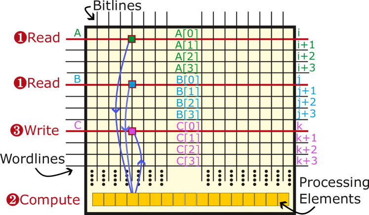
Bit-serial Processing-In-Memory (PIM) is a promising accelerator paradigm [12, 14, 20, 21, 28] with both high compute density and abundant on-chip memory capacity, especially considering the recent surge of demands on computing power and memory bandwidth in multiple application domains, including but not limited to deep learning, image processing, and signal processing. The essential principle of this paradigm is to integrate a single-bit processing element (PE) at the output of the sense amplifier under each bitline of a memory array so that massive data parallelism can be exploited over a transposed data layout.
This technology provides compute density that is competitive with the state-of-the-art GPUs. The theoretical throughput of a PIM system based on prior technologies [5, 12] is in the range of 310-340 GOPS/mm2 for int8 precision, for the same area and DRAM bandwidth as that of an NVIDIA A100 GPU. The GPU has a much lower vector throughput of 24 GOPS/mm2, but has a higher throughput of 755 GOPS/mm for Tensor Cores. However, Tensor Cores can only achieve high utilization for specific kernels and parameters. In addition, bit-serial PIM supports arbitrary precision, which can be extremely beneficial for saving memory bandwidth and increasing compute throughput. The paradigm keeps data near compute units to avoid data movement overhead and thwart the memory wall [42]. Overall, bit-serial PIM is a promising paradigm that has competitive compute density without needing specialized units like Tensor Cores, and can be a path-forward for DL workloads.
State-of-the-art PIM systems [14, 17] have showcased improved performance compared to previous generation GPUs. To make PIM systems outperform the state-of-the-art GPUs, we need to fully unlock the potential of the PIM paradigm by taking a system-level approach - co-optimizing hardware and software. Hardware should be carefully architected, given the area budget, to optimize computation and communication. Prior works suffer from excessively high overhead in on-chip data communication, because of lack of hardware specialization for common data access behaviors. Similarly, the software can be tuned to make better use of the underlying hardware. Prior works do not enable the software to take advantage of the hardware’s bit-serial nature to perform optimized data allocation and computation. Also, though some prior works claim to have a full-stack implementation, their programming interfaces are rather low-level. These interfaces limit the productivity of application development and performance tuning.
Our goal is to build a Processing-In-Memory (PIM) system - ISA, microarchitecture and compiler - that can exceed the performance and energy efficiency of similarly-provisioned GPUs and prior PIM systems, with a focus on DL workloads. There are two key principles that form the basis of our proposed design: 1. We optimize on-chip communications to be spatially-aware: H-tree interconnect topology for faster reductions at lower level of hierarchy & dynamic routing at higher level of hierarchy for scalability, explicit hardware for shuffling & multicasting operands for common data patterns in DL workloads, and systolic broadcasting. 2. We optimize the bit-serial computations that are common in PIM architectures: memory allocation can expand/shrink dynamically based on precision requirements (adaptive precision), large precisions can be broken down into smaller parallel computations (bit-slicing), and saving space & time by exploiting bit-level sparsity in operands for constant operations. Operations such as reductions, constant multiplication, multicasting, broadcasting are very common in workloads like DL.
Our overall system is a hierarchical and spatial PIM accelerator, abbreviated as PIMSAB. PIMSAB uses a hierarchical structure, where each tile is composed of many SRAM arrays capable of bit-serial PIM, along with an instruction controller that broadcasts commands to SRAM arrays in its tile. The ISA enables efficient expression of mixed scalar/vector program regions. The intra-tile network is simple and static for low overhead, and uses an H-tree [6] to facilitate high-bandwidth reduction. Broadcasting, multicasting, and shuffling mechanisms can be configured on this H-tree to reduce data packing overheads. At the inter-tile level, tiles communicate explicitly, and routing is done over a dynamically routed network to enable flexible parallelization strategies. Further, a mesh-based topology enables scalability to arbitrary sizes. PIMSAB’s programming interface is based on the TVM tensor DSL [10], which can be used to express a wide range of applications, including linear algebra, neural networks, and stencil processing. With moderate hints from the developers, the compiler can easily generate portable and high-performance code, by partitioning work across millions of PEs and balancing buffer occupancy and data parallelism.
Our evaluation shows that with sufficient co-design, PIMSAB can rival and surpass state-of-the-art GPUs as well as prior PIM systems. Specifically, we achieve 3 speedup over NVIDIA A100, while having 4.2 energy improvement for the equal-provisioned area and the same memory bandwidth. We also observe a speedup of 3.7 with similarly provisioned state-of-the-art SRAM PIM (Duality Cache), and a speedup of 3.88 with similarly provisioned state-of-the-art DRAM PIM (SIMDRAM). To sum up, the contributions are:
-
•
A hierarchical and spatial PIM system with an ISA, a microarchitecture, a compiler and a programming interface.
-
–
A microarchitecture that deploys dual-ported SRAM arrays with configurable PEs for PIM.
-
–
An ISA that exposes PIM-specific features of the hardware that can be utilized by the compiler.
-
–
A compiler that can automatically tune the parallelism and on-chip buffer allocation, with moderate hints from application developer.
-
–
A user-friendly programming interface using TVM Tensor DSL.
-
–
-
•
Employing techniques for spatially-aware communication (shuffle hardware, H-tree for efficient reduction, systolic broadcasting) and bit-serial-aware computation (constant operations, adaptive precision, bit-slicing) to achieve high performance.
-
•
Demonstration of GPU-outperforming performance and energy efficiency across both DL microbenchmarks and an end-to-end Deep Neural Network (DNN).
-
•
Comparison with state-of-the-art SRAM and DRAM PIM systems, showing improved performance for realistic benchmarks.
II Background
II-A Bit-serial Processing-In-Memory in SRAMs
Bit-serial computing paradigm performs operations on data bit-by-bit instead of element-by-element. This makes each operation take many cycles, but massive parallelism can be achieved by utilizing simple 1-bit processing elements, enabling high throughput.
Bit-serial Processing-In-Memory combines bit-serial computing with Processing-In-Memory. Analog approaches to bit-serial PIM [26, 23] require analog-to-digital and digital-to-analog converters, have high power consumption, and are therefore, not considered in this work. In digital approaches, 1-bit processing elements (PE) are added to an SRAM block. To provide operands to the PEs, two methods are used: (1) activating multiple wordlines at the same time on one port [1, 12, 3, 14], (2) using dual ported RAMs to read two wordlines at the same time [5]. Table I compares various properties of the compute capable SRAM blocks that use these two methods.
| Feature | Single Port Based | Dual Port Based |
|---|---|---|
| Activate two wordlines at the same time on one port | Yes | No |
| Requires extra voltage source | Yes | No |
| Requires extra row decoder | Yes | No |
| Requires modification to sense amps | Yes | No |
| Compute uses dual-port behavior | No | Yes |
| Generic/Flexible PE | No | Yes |
| Cross-RAM shift | No | Yes |
| Area of the array | Lower | Higher |
| Frequency of operation | Lower | Higher |
| Examples | [1, 12, 3, 14] | [5] |
Figure 1 shows the basic principle of bit-serial Processing-In-Memory. In every cycle, two wordlines containing a bit of each operand are activated, the processing element performs the computation and the result is written into a wordline. Operations such as addition, multiplication, etc. can be performed by repeating this basic step over multiple cycles. We refer the reader to Neural Cache [12] for a detailed description of the algorithms for various operations. Note that floating point and transcendental operations are also supported [20, 14].
The challenges in prior PIM systems include (1) high on-chip communication overhead in moving partial results across the chip and in organizing the data in the right layout, especially in large systems with thousands of RAMs, even though the off-chip memory traffic is reduced, and (2) bit-serial computation takes a large number of cycles, especially when the precision expands because compilers allocate the number of bits based on traditional paradigms (e.g. int8 int8 int32) .
II-B Tensor Domain-Specific Language (DSLs)
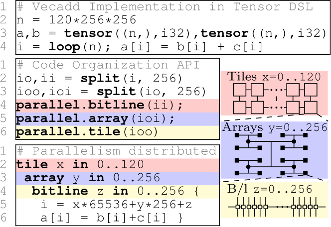
DSLs, like Halide [33], TVM [10], and Tensor Comprehensions [39], are developed to productively write high performance tensor programs. The idea is to decouple the algorithm and the performance tuning controlled by loop re-organization. Consider the vector addition implementation in Figure 2: Loop variables and tensors are first declared, and then a vector addition is implemented in an expression involving these declared variables. Using the DSL allows us to tune the algorithm at an abstract level orthogonally with the specific problem tiling and work distribution that is involved when realizing it on a specific hardware. By tiling, ordering, and annotating the loops, the parallelism in the program can be mapped onto our hardware hierarchies.
III Overview
III-A Hardware Organization
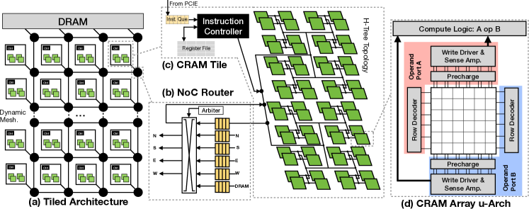
Figure 3 provides an overview of the hardware organization of PIMSAB. The PIMSAB hardware deploys a large number of compute-enabled SRAMs (or CRAMs). Each CRAM is a dual-ported SRAM modified to add multiple single-bit PEs. We base our CRAM design on CoMeFa [5], because of its more practical design compared to Neural Cache [12]. We use their basic block to build a large scalable network of CRAMs with several enhancements for both communication and computation, enabling efficiently at scale.
To communicate between the CRAMs, a statically scheduled network is chosen, since most communication patterns are identifiable at compile time. We choose an H-Tree topology for this network, because it is well suited for partial sum reduction, a common computation pattern in DL and many modern applications. Statically scheduling the entire chip would put too much burden on the compiler. So, we introduce another level of hierarchy: tiles. Tiles communicate using a dynamically scheduled packet-switched NoC. We choose a 2D mesh topology for the NoC because this enables scalability. The NoC is used to send and receive data across tiles and to/from DRAM. Having parallelism at 3 levels of hierarchy - CRAM, tile, chip - enables PIMSAB to capture different types of parallelism in highly data-parallel applications.
Each CRAM needs to be fed micro-ops to perform computation. An instruction controller decodes the instructions and provides micro-ops to the CRAMs every cycle. However, connecting an instruction controller to each CRAM would result in significant overhead. We reduce this overhead by having one instruction controller in a tile, making CRAMs in each tile operate in a SIMD fashion.
The PIMSAB system defines three memory locations: main memory (DRAM), CRAMs and register file. HBM (High Bandwidth Memory) DRAM is adopted to sustain the high bandwidth required by massive parallelism. To simplify physical design, DRAM controllers are connected to the routers at the edges of the NoC. For similar reasons, we connect all DRAM controllers to the top edge of the mesh NoC. A register file is provided in each tile to store constants or scalars. We assume a PCIe interface, both for loading instructions and for transferring data (like GPUs).
III-B Enabling Scalable and Performant Processing-In-Memory
In this section, we present the innovationse - for spatially-aware communication and for bit-serially-aware computation - that make PIMSAB a scalable and performant PIM system.
Register File and Constant Operations: A frequent operation in applications such as DL is multiplying a scalar (or a constant) with an array or vector operand. With the computation paradigm of bit-serial PIM, we would have to replicate this scalar over multiple bitlines in the CRAM. A more efficient way is to keep scalars outside the CRAM and perform what we call constant multiplication (explained in Section IV-B). To store these scalar operands, we introduce a register file (RF) in each tile. Additionally, this approach can enable exploiting bit-level sparsity in the constant operand by skipping operations for zero-bits, leading to up to 2 speedup in operations like multiplication and 4 speedup in operations like dot product. This feature is exposed to the compiler through the ISA (mul_const instruction).
Dedicated Shuffle Hardware: When data is loaded from the DRAM, it often needs to be broadcasted or multicasted to various CRAMs in different patterns to avoid loading data multiple times or to ensure high utilization of CRAMs in a tile. In addition to just loading data from DRAM, broadcasting or multicasting is useful when data is transferred from one tile to another. We provide explicit hardware near each CRAM to support this. Several multicast and broadcast patterns are supported, governed by the requirements of common workloads such as GEMM. Pattern specification is exposed to the compiler through special fields in the data transfer instructions.
Adaptive Precision: Since PIMSAB uses bit-serial operations, any precision is supported, including floating point. In PIMSAB ISA, the precision for each operand can be specified separately. This capability of specifying a custom precision at operand granularity enables using just the number of bits that are required and allocating only the required number of wordlines. For example, when multiplying numbers of precision 8 and 10, 18 wordlines can be allocated to store the result, instead of 32 bits as in a normal CPU. Our compiler exploits this feature to pack as any operands as possible in each bitline (enabling high reuse), even splitting portions of an operand across non-consecutive wordlines.
Bit Slicing: Although bit-serial PIM can support any precision, the number of cycles consumed by an operation directly depends on the precision of the operands. Larger precisions (e.g. int32) take more cycles than smaller precisions (e.g. int8). However, in PIMSAB, we employ a technique where larger precision operations are broken down into smaller-precision independent parallely-executable operations and the results are combined later. We refer to this as bit slicing. For addition, this is exposed to the compiler by a special field in the instruction. For multiply, this is done by the compiler in software.
Cross-CRAM Shift: Shifts are commonly used in operations like stencils, filters, etc. Vectorization widths in PIM architectures can get really large (e.g. in PIMSAB, the vectorization width for maximum utilization is 256*256). Supporting only intra-CRAM shifting (i.e. shifting data from a bitline to the next within a CRAM using connections between PEs) limits the utility of the shift operation to only a CRAM. To support shifting data from a bitline to the next across the whole vectorization width, we provide CRAM-to-CRAM shift connections within a tile. This gives PIMSAB the ability to perform filters and stencils much more efficiently.
Systolic Broadcasting: Chip level communications, such as broadcast, are essential for workloads such as convolutions, where weights need to be broadcasted to multiple compute units or tiles. However, naive broadcast algorithms, like one-to-many transfers, can cause extreme network congestion and overheads. To optimize this, we support a near-neighbor systolic-like data transfer supported in hardware and exposed to the compiler through the load_bcast and tile_bcast instructions. This efficiently utilizes the available NoC bandwidth and reduces congestion.
Hierarchical Interconnect: A two-tiered interconnect is used in PIMSAB. A statically scheduled H-tree interconnect topology at the lower (intra-tile) level is used to enable faster reductions. A dynamically scheduled mesh interconnect topology at the higher (inter-tile) level is used to reduce the burden on the compiler and also to increase the scalability of PIMSAB. A non-hierarchical PIMSAB would mean one of two implementations: (1) All CRAMs connected using a static H-tree interconnect. This would lead to excessive burden on the compiler because the whole computation would need to be statically scheduled. Additionally, this would cause a rapid degradation in the frequency of operation of the chip as the number of CRAMs increases. (2) All CRAMs connected using a dynamically routed mesh network. This would imply one router for each CRAM, increasing the area overhead of non-computational logic significantly. In either implementation, we would need one instruction controller per CRAM. Area overheads of each unit are shown later in Section VII-H.
IV Architecture
IV-A Instruction Set Architecture (ISA)
In this section, we elaborate the PIMSAB ISA, including Compute, Data Transfer and Synchronization instructions.
Compute Instructions: Compute instructions support arithmetic and logical operations, operate on data in the CRAMs, and are vectorized across bitlines. We also support inter-bitline instructions, like shifting data across bitlines. Instructions to reduce data within a CRAM and across the CRAMs in a tile are also provided. We also have an instruction, set_mask, which copies the data of wordline into the mask latches in PEs, to enable predicating operations per bitline. Additionally, each instruction has a field to specify what should be used for predication - the mask latch or the carry latch (Section IV-B describes the PE architecture incl. the latches). In most cases, all compute instructions are executed across all the CRAMs in tile, but we also have a field (called size) to specify the number of bitlines involved in the operation across the tile.
Bit Slicing: To support bit slicing, in the add instruction, we provide two special fields. The cen field can be used to specify if the carry stored in the PE (from a previous op) should be used during the first step. The cst field can be used to specify if the generated carry in the last step should be written into the CRAM. This allows larger precision addition operations to be broken down into smaller precision operations by the compiler much more efficiently. For example, to perform an 8-bit addition, two separate 4-bit additions can be performed, and the second 4-bit addition can directly use the CARRY bit from the first one. Also, for multiplication ops, bit slicing is done at the software level by the compiler, which divides-up large operands, performing the individual ops in parallel and reducing the results.
Operations with scalars or constants: For multiplication operation, a special instruction called mul_const is provided where one operand is from the RF (scalar or constant), instead of being replicated in the CRAM. This instruction skips zeros in the constant operand in the RF, reducing the execution time.
Data transfer instructions: These instructions are used to move data between the DRAM, CRAMs and the RF. Specifically, we support bidirectional data transfer between DRAM and CRAMs, as well as DRAM and the RF. An instruction to send data from one CRAM in a tile to another is also provided. In addition, we also support data loaded from DRAM to be broadcast to multiple tiles’ CRAMs. Within each tile, we allow one CRAM to broadcast data to all other CRAMs. Tiles are allowed to perform either point-to-point communication or broadcast data. Point-to-point communication blocks the receiver until the data arrives.
Synchronization instructions: These instructions coordinate data transfers and computations among tiles. Two synchronization instructions provided are signal and wait. signal sends a message from a source CRAM to a destination CRAM and is non-blocking. A CRAM can wait for a message (blocking) from a source CRAM using the wait instruction.
Transposing data: In load and store instructions, besides the source address, destination address, size and precision, there is an additional tr field specifying if the data is transposed or not. This can be used when, e.g., an immediate/constant operand read from the main memory need not be transposed.
Program example: A simple elementwise vector multiplication is shown in Listing 1. The program generates an instruction stream for all tiles in the chip (NUM_TILES). Two operand arrays, each with elements of precision int8, are loaded from the main memory. vec_width is specified to be the full width of a tile. Then a multiplication instruction is used to generate a result with precision int6. The result is then stored back to main memory.
IV-B Microarchitecture
Here we discuss PIMSAB’s microarchitecture. Table II provides a list of hardware parameters.
| Parameter | Value |
|---|---|
| CRAM geometry | 256x256 |
| PEs per CRAM | 256 |
| CRAM size | 8 KB |
| Mesh dimensions | 12x10 |
| DRAM bandwidth | 12288 bits/clock |
| Clock frequency | 1.5 GHz |
| Num tiles | 120 |
| Num CRAMs per tile | 256 |
| Total CRAMs | 30720 |
| RF size | 32 32-bit regs |
| Tile-to-Tile bandwidth | 1024 bits/clock |
| CRAM-to-CRAM bandwidth | 256 bits/clock |
CRAMs: We employ dual-ported compute-enabled RAMs (called CRAMs). A CRAM has two modes: compute and memory. In compute mode, the data word written into the memory is treated as a micro-op. Each micro-op takes 1 cycle, in which two wordlines are read, computation is performed in the PE, and the result is written into a wordline. In memory mode, the CRAM behaves as a normal RAM. CRAMs are grouped into tiles; all CRAMs in a tile execute in lock-step in a SIMD fashion (except when executing CRAM-to-CRAM data transfer). CRAMs in a tile are connected through the intra-tile network. In addition, there is a single wire ring interconnect between all CRAMs in a tile to facilitate shift instructions.
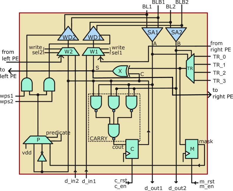
Processing Element (PE): PIMSAB adopts the PE architecture from CoMeFa [5], as shown in Figure 4. Each PE can perform any logical operation between 2 operands, using the TR mux. With the addition of an XOR gate (X), it can also perform a 1-bit full adder operation. A carry latch (C) is used to store the carry-out, which can be used as carry-in for the next timestep. The output of the TR mux can be stored in the mask latch (M). Predication based on mask bits and carry bits is supported, through the predication mux (P). There are as many PEs in a CRAM as many bitlines. The operation performed by the element is governed by the micro-op received by the CRAM from the instruction controller.
Instruction controller: Instructions are received from the HOST over PCIe. Each tile has an instruction controller to decode and farm-out execution to corresponding units. For compute instructions (add, multiply, reduction, etc.), it generates micro-ops for the CRAMs every cycle. For data transfer instructions (CRAM-to-CRAM transfer, tile-to-tile transfer, DRAM transfers), it reads the CRAM and sends data into the static network’s switches, and also writes data coming in from the switches into the CRAMs.
On-chip networks: The inter-tile network uses a standard wormhole-switched dynamic NoC, with X-Y routing. The intra-tile network is a static circuit-switched network using an H-Tree topology. This is similar to a hierarchical FPGA [2, 37], but with much smaller configuration overhead because of the coarser granularity (word-level instead of bit-level). Each switch is a buffered crossbar with 5 input and output ports. Each output port can be driven by the other 4 input ports, controlled with 2 configuration bits. This network only needs to be reconfigured if there is a data transfer instructions with new communication pattern; this is rare for tile-to-tile transfers and DRAM transfers.
Shuffle logic: To facilitate operations like GEMM and convolutions, different data layout patterns are required. E.g. we may need a data element to be duplicated in each bitline or repeated every 4 bitlines in a CRAM. Such data layouts help data reuse and avoid unnecessary data traffic from/to DRAM. For this purpose, at the periphery of each CRAM, a shuffle logic unit is provided. Data can be shuffled before writing into the CRAM. The shuffling pattern is an input to this shuffle logic and is exposed to the compiler through the shf argument in the tile_bcast and load_bcast instructions. shf specifies the stride of distributing the bits of data received onto the CRAMs in the tile. E.g., a 256-bit value loaded from DRAM into a tile can be shuffled such that the first bit is duplicated in 256 bitlines in the first CRAM, the second bit is duplicated in 256 bitlines in the second CRAM, and so on.
DRAM interface and transpose unit: All tiles in the top-row of the mesh NoC are connected to DRAM controllers. The data from DRAM must be transposed before storing into CRAMs, so that bit-serial arithmetic can be performed. Results need to be untransposed when writing back. We use a transpose unit similar to CoMeFa’s [5]. It employs a ping-pong FIFO. Data enters from one side into the ping part in the non-transposed format. When full, transposed output is obtained by reading bit slices of the loaded elements, while the pong part is filled with new data. When the pong part is full, the roles are reversed and the process repeats. In PIMSAB, this unit is integrated within the DRAM controller(s). This unit can be disabled if not needed (through the tr field of the DRAM load/store instructions), e.g. for the weights of a neural network, which can be pre-transposed.
Register File and operations with constants: Each tile has a register file (RF) that stores data in untransposed format. RF is used in performing operations with scalars or constants. When an instruction (mul_const and add_const) is issued, the instruction controller fetches the scalar operand from the RF and sends micro-ops to the CRAMs according to the bits of the constant which are set. This saves the overhead of copying the same operand to multiple bitlines in the CRAM. It also speeds up the computation by exploiting bit-level sparsity through skipping some micro-ops. For example, for multiplication, if a bit of the scalar operand is 0, all micro-ops for summing the partial products for that bit position can be skipped. Finally, we enable parallel RF writes for quickly loading constants. Thus, we use a flip-flop based design to avoid port restrictions.
V Compiler
V-A Overview
Programming Interface
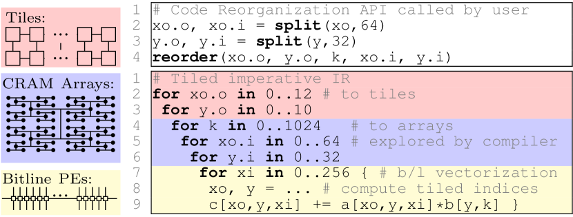
We adopt a tensor DSL as our high-level interface, because of its portability and ease of performance tuning. As shown in Figure 5(a), a matrix multiplication is implemented in a tensor DSL, by declaring loops, and tensors, and describing the program behaviors in expressions involving these declared variables. The loop organizations are the key to the performance tuning in tensor programs, and can be easily explored by invoking several loop organization primitives (e.g. split and reorder shown in Figure 6). The parallelism is naturally encoded in the declared loops with different types, either data-parallel or reduction. These different loop types may lead to different program behaviors when mapping loops to different hardware hierarchies.
Performance Tuning
Different implementations significantly affect the on-chip buffer occupancy, memory traffic, on-chip network traffic, and parallelism distribution, and lead to different performances. Considering the excessively large space of code organizations, we decide to leave part of the performance tuning as developers’ responsibility, including the loop organization and data layout, so that the compiler can figure out the best parallelism distribution and buffer allocation under this organization.
To explain, consider the matrix multiplication example in Figure 5(a). Its imperative version in Figure 5(a’) shows that the innermost reduction loop across is hard to be parallelized across bitlines specialized for vector parallelism. Thus, one important transformation is to place a data-parallel dimension in the inner loop. As shown in Figure 5(b)&(b’), the outermost dimension of tensor a is tiled by 256, and reordered to the innermost for mapping to bitline PEs. Then, Figure 6 shows that users are required to call the loop organization APIs to determine a code organization for the compiler to distribute the parallelism and allocate CRAM memory buffers.
Compiler Optimizations
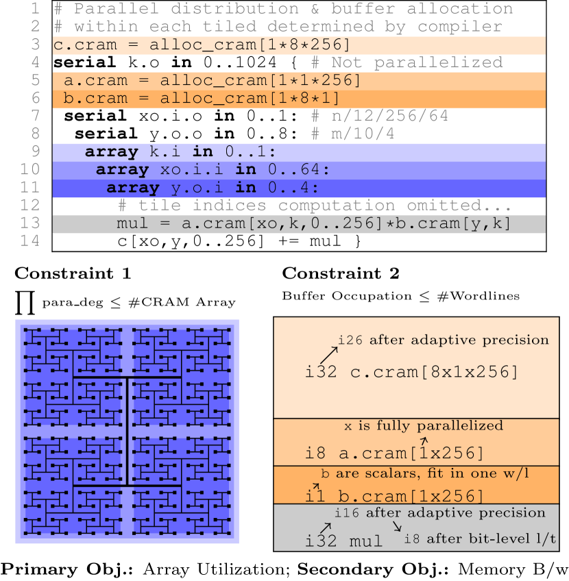
After the data layout and loop organization are determined, the compiler analyzes the program and optimizes it. The optimization includes both coarse grain optimizations (in Section V-B) like distributing parallelism to hardware hierarchies, and memory buffer allocation, as well as fine grain optimizations (in Section V-C) that take advantage of the properties of bit-serial arithmetic to save on-chip memory occupancy. Since the exploration space of coarse-grain optimizations is small, the compiler exhaustively evaluates each point, and adopts the one with the best objective. As shown in Figure 7, the parallelism distribution will affect the memory buffer allocation. If the required buffer size exceeds the on-chip resources available, this exploration point is considered invalid. To make more exploration points more likely to succeed, fine-grain optimizations will squeeze the buffer size requirement.
Code Generation & Feedback Loop
After the favored parallelism distribution and buffer allocation is successfully determined on the given loop organization, the compiler extracts all the computational instructions to be offloaded to PIM and rewrites them in hardware intrinsics. Then the transformed IR is ready for code generation. If all the parallelism distribution fails under the given loop organization, the compiler will throw an error to the developer, and the developer is required to find another more conservative loop organization.
V-B Parallelism Distribution & Memory Allocation
Parallelism distribution determines how much of these loops should be tiled and parallelized across hardware hierarchies, and how much should be executed in serial. Since the parallel degree of each hierarchy is at an order of hundreds, the loop tiling space is small enough for the compiler to search exhaustively. Next, we explain how the loops are mapped to parallelism across and within tiles.
Inter-Tile Parallelism Distribution
Considering the overhead of communicating data between tiles, it is often inefficient to reduce the partial sum across different tiles. Therefore, our compiler only seeks to map data parallel loops to inter-tile parallelism. Assuming we have 120 tiles, each iteration of xo.o and y.outer in Figure 6 are mapped to each tile exactly. If the iterations exceed the number of tiles, the compiler will seek to tile the loops and execute parts serially.
Intra-Tile Parallelism Distribution
Figure 7 shows that, after the inter-tile parallelism is fixed, the compiler distributes the intra-tile parallelism by exploring the space of loop tiling. Each tiled outer loop (with .o suffix) will be executed in serial by each tile’s controller, and each tiled inner loop (with .i suffix) will be mapped to a CRAM array. The total iterations of these .i-loop should not exceed the number of arrays. This can easily be enforced when tiling the loop by multiplying the tiling factor. Besides, the CRAM buffer allocation should not exceed the wordlines available in each array.
When there are multiple distributions that fulfill these two constraints (parallelization degree and CRAM buffer), we use two objectives to determine the best one. The primary objective is more computing resource occupancy, and the second is less DRAM memory bandwidth. The rationale behind this objective order is that a high computing resource occupancy often requires high data bandwidth to sustain.
CRAM Buffer Allocation
CRAM buffer allocation is the key to determine the feasibility of a parallel distribution. Here, we first explain how the compiler greedily exploits data reuse, and compute occupancy, while not exceeding the CRAM capacity. Some overused CRAM capacity can be false positive, the compiler will try to detect and optimize it. If it turns out to be a true overuse, a feedback will be sent to the developer for a conservative initial loop organization.
For the example shown in Figure 7, the compiler greedily allocates the memory buffer at the highest serialized loop with reuse. Therefore, a and b are allocated below k.o, and c is allocated above k.o. Then, the compiler tries to minimize the CRAM buffer occupancy by analyzing the data access pattern of each operand. In the case shown in Figure 7, the size of each buffer is proportional to the iterations of serialized loops. For example, because the indices of c are controlled by xo and y, the c.cram buffer size is 1832, where 1 is the serial iteration of xo.i.o, 8 is the serial iteration of y.o.o, and 32 is the precision of the integers. Similar thing happens to a.cram: because its index is only controlled by xo (k is ignored, because there is no reuse over k), its buffer size is 18. Therefore, parallelizing xo.i is more favored, because it save more buffer occupancy for both a&c, considering b.cram are all scalars. After fully parallelizing xo.i, y.o is further parallelized to fill the remaining arrays for compute resource occupancy. Finally, c’buffer, 1x8x32=256 wordlines, already occupies each entire CRAM array, with no space remaining for other operands, intermediate values, which indicates the unfeasibility. However, it is a false positive. In the next section, we will explain how we squeeze the CRAM allocation to optimize this false overuse.
V-C Optimizing CRAM Data
Here, we focus on optimizations within each CRAM. False overused CRAM allocation can be optimized so that potentially more aggressive parallel distribution can be feasible.
For the example in Figure 7, 32x8=256 wordlines are required for the accumulated results (c.cram), 8x1=8 wordlines for the operand a, 1 wordline for the operand b, and implicit 32 wordlines for the intermediate results. In total, 256+8+32+1=297 wordlines, which exceeds 256 wordlines of each array. Next, we will explain how our optimizations make them fit. These optimizations mostly take advantage of the divisible nature of bit-serial arithmetic — each bit of results is independently accessible.
Adaptive Precision
This technique can save memory space of the computed results. The minimum feasible precisions are adopted to override the precision in the original program: Multiplying an -bit and a -bit number is at most bits; accumulating -bit numbers requires only + bits. Specific to the example shown in Figure 5, though the results are accumulated on i32, only i26 is required. The input operands are both i8, so the result of multiplication is within i16. We now have p=1024 i16 accumulated, in total 1024+16=26 bits for each accumulation. Therefore, we in total saved (32-26)x8+16=64 wordlines, so now only 249 wordlines are required.
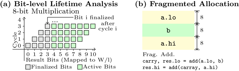
Lifetime Analysis
The divisible nature of bit serial arithmetic makes each bit have its own lifetime. We extend the code scheduling in CHOPPER [32] to an even broader applicability. For a multiplication that is consumed immediately by an addition, instead of keeping the whole 16 bits of multiplication, we can add it to the accumulator as soon as a bit is finalized. As shown in Figure 8(a), after i cycles of multiplication, the i-th bit is finalized, and it always maintains a half-width active window when doing a multiplication. Therefore, this saves 16/2=8 wordlines, and now we only occupy 243 wordlines.
Fragmented Allocation
Fine-grain lifetime analysis will lead to fine grain memory recycling, which makes fragmentation more likely. This can hurt the utilization badly in conventional memory allocation. However, the divisible nature of bit-serial PIM allows us to allocate fragmented memory. We also need to divide operands and associated operations into fragments, so that even tiny fragments can be utilized when required. Figure 8(b) shows an example of fragmented allocation. a is divided into two fragments straddled by b, and fragmented operations are generated for this allocation.
Data Loading & Packing
Once parallelism distribution passed the constraint check after these optimizations, the compiler will then inspect the memory access pattern to generate code for data loading and packing. If several tiles are using the same data, the common memory traffic will be converted to on-chip network communication. The compiler also analyzes the the operands loaded to the CRAM arrays to determine how they should be broadcast and shuffled through the H-tree. For example, xo is not related to reading b.cram[y,k], so loaded b should be broadcast to all the arrays mapped to different iterations of xo.
V-D Implementation
We integrate our compiler analysis and transformations to the TVM compilation flow. TVM provides rich code organization primitives to tune loop organizations and allocate memory buffers. We start with the initial code organization provided by user, and apply our explored parallelism and memory allocation. This is lowered to an IR with all the loops and buffers instantiated. Then CRAM data optimization is done on this level of IR. If the memory occupancy satisfies the hardware constraints, all the arithmetic operations are rewritten in bit-serial intrinsics, including arithmetic operations, memory loading, and data transfer, which are ready for code generation. If not, we invoke a feedback loop to explore a more conservative code organization for less memory occupancy.
VI Evaluation Methodology
VI-A Modeling PIMSAB
Performance
We develop a cycle-accurate simulator in C++ to model the PIMSAB hardware. The simulator executes a program written in the ISA described in Section IV-A. An input configuration file is used to specify various parameters of the microarchitecture. Various metrics like cycles and energy breakdown by each component or instructions can also be reported by the simulator.
Area and energy model
We develop an area and energy model to fairly compare PIMSAB against our baseline, the NVIDIA A100. We write Verilog RTL for the static H-tree network, shuffle logic, instruction controller, transpose unit, and register file. For RAM blocks, we use the OpenRAM memory compiler [16]. We verified and synthesized using Synopsys VCS and DC (using FreePDK45[30]) to obtain post-synthesis area and power. We further assume a 15% area overhead for place and route[19]. For the PEs in each RAM, we write transistor level code and evaluate area and energy using SPICE with 22nm ASU PTM technology [38]. For the dynamic NoC, we use PAT-Noxim simulator [31] and extract area and energy values for the routers and links. For the on-chip DRAM and PCIe controllers and transceivers, we obtain areas from A100 die analysis. For DRAM energy, we use a simple analytical model calibrated from memory-only microbenchmarks on the A100. We scale all values, for both PIMSAB and A100, to 22nm using scaling factors for area, power and delay from [36].
VI-B Configurations
GPUs are the most common commercially available accelerators for DL workloads; so we compare PIMSAB against NVIDIA A100 GPU. Additionally, we compare against state-of-the-art prior SRAM and DRAM based PIMs (DualityCache and SIMDRAM). To make fair comparisons, we build three different PIMSAB configurations for each of the comparisons.
NVIDIA A100 GPU
We provision PIMSAB to have the same area (825mm2 in 7nm, i.e. 2950 mm2 in 22nm) and DRAM bandwidth (12288 bits/cycle, i.e. 1866GB/s @1215 MHz). GPU performance is measured by running on an A100 using NVIDIA’s profiler NSight Compute. Each kernel is measured by averaging 500 launches to exclude the device overhead. To compare the dynamic energy of PIMSAB with A100, the static energy is normalized indirectly to A100 through having the same area footprint and DRAM bandwidth. Table III describes the benchmarks we use and their characteristics. 5 highly parallel kernels from high performance libraries, including ArrayFire[43] (fir), and CUTLASS[27] (gemm, gemv, conv2d) are used as microbenchmarks. These microbenchmarks use integer datatypes. We choose different precisions for different benchmarks to demonstrate precision agnosticism. We use quantized Resnet18 from MxNet Model Zoo to demonstrate the capability of targeting end-to-end workloads.
| Benchmark | Size | Precision | Comparison |
|---|---|---|---|
| vecadd | input=15728640 | int8 | A100 |
| fir |
input=7833600,
filter=32 |
int16, acc=int16 | A100 |
| gemv | m=61440, k=2048, n=1 | int8, acc=int32 | A100 |
| gemm | m=61440, n=32, k=2048 | int4, acc=int16 | A100 |
| conv2d | input=9x9x256x2, weights=3x3x256x256 | int8, acc=int32 | A100 |
| resnet18 |
input=224x224x3x1,
output=1000x1 |
int8, acc=int32 | A100 |
| backprop | input=65536x16 | fp32 | DC |
| dwt2d | input=1024x1024 | fp32 | DC |
| gausselim | input=256x256 | fp32 | DC |
| hotspot | input=1024x1024 | fp32 | DC |
| hotspot3d | input=512x512 | fp32 | DC |
| vgg13 |
input=224x224x3x1,
output=1000x1 |
binarized | SIMDRAM |
| vgg16 |
input=224x224x3x1,
output=1000x1 |
binarized | SIMDRAM |
| lenet |
input=32x32,
output=10x1 |
binarized | SIMDRAM |
Duality Cache (DC)
DC has 1.14 million processing elements and runs at a frequency of 2.6 GHz. We design a PIMSAB chip (PIMSAB-D) sized to match the compute throughput of DC for a fair comparison. PIMSAB-D has 30 tiles (organized in a 6x5 mesh). The CRAM size for DC is the same as for PIMSAB (256 bitlines x 256 wordlines). DC uses Rodinia [9] benchmarks and hence we use the same for this comparison.
SIMDRAM
We also compare PIMSAB to SIMDRAM [17]. We use the 1 bank configuration mentioned in their paper. We design a PIMSAB configuration (PIMSAB-S) with a lower number of processing elements in PIMSAB to match those in SIMDRAM. PIMSAB-S has 1 tile. We use 3 full Deep Neural Networks (LeNet, VGG-13, and VGG-16) as benchmarks for comparison since they were used in the SIMDRAM work.
We do not build performance models of the DC and SIMDRAM architectures. Instead we obtain the raw runtimes for the benchmarks they used by directly reaching out to the authors, and used those for comparison.
VII Results
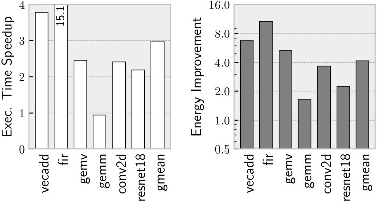
VII-A Comparison with state-of-art GPU
Figure 9 shows the execution time and energy comparison against NVIDIA A100 GPU. On average, PIMSAB outperforms A100 by 3 in execution time, and 4.2 in energy. The two main sources of the speedup are: (1) the high fine-grain data parallelism in PIMSAB leads to reduced instruction overhead, and the larger on-chip buffer (512 MB on PIMSAB vs. 96 MB, including L2, shared memory and RF, on A100) leads to more data reuse and reduces off-chip memory traffic.
PIMSAB significantly outperforms A100 on fir because of the unaligned memory access caused by the sliding window. In PIMSAB, this program behavior can easily be handled by shifting bits across bitlines, while it prevents the GPU from fully utilizing the memory bandwidth. PIMSAB can achieve almost the same performance as A100 for gemm, even though A100 uses Tensor Cores for GEMM, which provide peak GOPs compared with PIMSAB.
VII-B Comparison with SRAM PIM (Duality Cache)
Fig 10(a) shows PIMSAB-D outperforms Duality Cache by 3.7 on average across several Rodinia benchmarks. PIMSAB-D shows speedups over Duality Cache on backprop, hotspot2d, and hotspot3d, because of the tensor DSL programming compiler can easily analyze the memory footprint and allocate buffers for memory reuse. In addition, Duality Cache still adopts a GPU-like warp-wise execution, which imposes high overhead to coordinate unaligned data loading. PIMSAB can simply shift across bitlines, even across CRAMs in a tile, so it outperforms DC on dwt2d. gaussian-elim is bound by memory packing on DC, but our hardware is well specialized for it because of the H-tree, which also leads to fewer computational instructions.
VII-C Comparison with DRAM PIM (SIMDRAM)
Fig 10(b) shows our comparison against SIMDRAM. PIMSAB-S outperforms SIMDRAM [17] by 3.88 on average across real world neural networks, because in-SRAM processing takes advantage of data reuse in on-chip buffers. SIMDRAM has to pay DRAM read latencies for every computation and is at a disadvantage for workloads with data reuse. PIMSAB’s speedup is lower on LeNet because the LeNet model is relatively small — SRAM-DRAM transfer occupies a larger portion of execution, compared to the other networks.
VII-D Time and energy breakdown
Figure 11(a) shows the breakdown of time spent in each benchmark. Since vecadd has low arithmetic intensity, most of the time is spent on DRAM loads and stores, as expected. In fir, about 60% of the time is spent on DRAM traffic. gemv is also DRAM bound because of low reuse. gemm and conv2d are dominated by network traffic, because our compiler’s loop organization transformation objective is to minimize the estimated DRAM traffic by converting them to network data transfer. resnet18 is mainly a sequence of convolution layers followed by elementwise operations. We see that more time is spent on computation in resnet18 than a standalone convolution layer. This is because elementwise layers (1) often have higher precision than convolution, and (2) underutilize the hardware because of inter-CRAM reduction.
Figure 11(b) shows the breakdown of energy consumed in each benchmark. vecadd, fir and gemv are dominated by DRAM energy because of the limited reuse. In microbenchmarks like gemm and conv2d, around 40% of the energy is spent on computation. For resnet18, even though 20% of the time was spent on compute, 10% energy is spent on computation.
VII-E Sensitivity to different hardware parameters
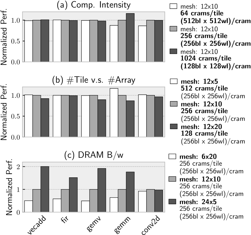
As shown in Figure 12, we analyze a set of 7 different hardware configurations, obtained by varying 3 hardware parameters, with the microbenchmarks. Figure 12a studies the sensitivity of number of compute resources (PEs) by tuning the size of each CRAM while retaining a constant memory capacity. Assuming each CRAM is a square (#wordlines=#bitlines), halving the number of bitlines results in 4 more compute intensity (more PEs for the same amount of memory). However, according to the cycle breakdown shown in Figure 11(a), the computations occupy a small portion (on average less than 20%) of the execution time. So, increasing the compute resources without increasing memory capacity only slightly improves the performance by 2.6%, and decreasing the compute resources slightly hurts performance by 5.4%.
Figure 12b studies the tradeoff between the number of tiles and CRAMs per tile, while retaining the same number of compute resources. Increasing the number of tiles implies a larger dynamic network (NoC), and increasing the number of CRAM per tile means more static network. The results of this study suggest that more tiles hurt performance by 8.2%, and larger tiles provide dimishing returns (~1.5% improvement).
Figure 12c shows the tradeoff by changing the memory bandwidth. This is achieved by changing the mesh geometry, since only the top-row tiles have memory controllers. The massive data parallelism requires massive data to sustain. Therefore, workloads with poor reuse, like vecadd, and gemv, which are bounded by memory accesses, achieve nearly linear speedup when doubling the memory bandwidth (i.e number of columns in the mesh is doubled). Although according to Figure 11(a), gemm’s execution time is not dominated by DRAM bandwidth, the performance is significantly improved when number of columns in the mesh increases. This speedup is attributed to reduced data transfer time because the mesh height is reduced to half. conv2d is an outlier; the performance is not affected (even slightly lowered) by the memory bandwidth increase. Because of the shape of the kernel (), we could only partition the memory load across tiles and broadcast them to all the tiles, which means memory controllers are not fully utilized and loaded data is broadcasted to further tiles because of the wider mesh width. Overall, although more memory bandwidth is beneficial, for an iso-area and iso-memory-bandwidth comparison to the A100, we choose the configuration with mesh as our main configuration.
VII-F Sensitivity to different workload parameters
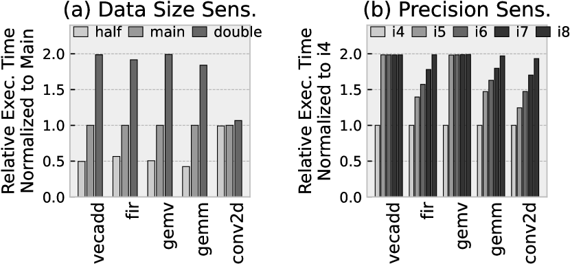
Figure 13(a) shows the sensitivity of PIMSAB’s performance to workload sizes, by studying 2 additional sizes i.e. halving and doubling the data. The execution time of workloads with limited data reuse (e.g. vecadd and gemv) is linearly proportional to the data size. Same is the case with gemm and fir; they have better hardware utilization in larger sizes because of data reuse. Because of compute underutilization caused by shapes, conv2d performance does not vary much with input size.
Figure 13(b) shows the sensitivity of PIMSAB’s performance to the precision of the inputs. A unique capability of bit-serial systems is to support any arbitrary precision. We vary the input precisions from 4-bits to 8-bits. Since the DRAM representation always aligns to a power of 2, the DRAM traffic remains the same for int5 to int8. Thus, the DRAM bound benchmarks (vecadd and gemv) exhibit the same performance under those precisions. Because computation and on-chip network traffic constitute a considerable amount of the execution time in fir, conv2d, and gemm, the performance of these workloads changes nearly linearly with precision. Note that adaptive precision eliminates the requirement to utilize 8-bit computations for smaller precisions.
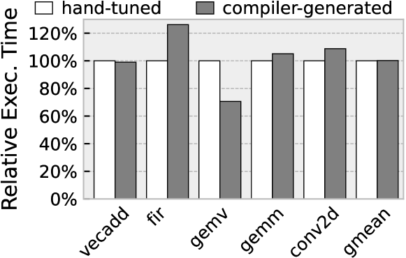
VII-G Quality of compiler-generated code
With the goal of validating our compiler, Figure 14 compares compiler-generated code with hand-tuned code. The geomean performances are nearly the same. fir, gemm, and conv2d, are moderately slowed down, because our compiler conservatively generates code for the synchronization between receiving broadcasted data and computation, which serializes these two phases. Manually coded versions can fine tune this part of overhead to reduce data transfer. In gemv, our compiler outperforms the hand-tuned code, because as discussed in Section V, the compiler avoids inter-tile communication for compute reduction to save significant overhead on NoC communication. The hand-tuned code, however, uses a sub-optimal algorithm.
VII-H Chip Area Distribution
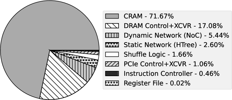
Figure 15 shows the area distribution of the PIMSAB chip. 72% of the chip area is consumed by the CRAMs, indicating a large percentage of useful compute/storage area. The dynamic and static networks take 7.5% of the chip area, while the shuffle logic occupies 1.5% of the area. The DRAM controller, transpose units and transceivers (XCVR) occupy 17% of the chip. Considering the additional capabilities enabled by PIMSAB, the overhead is relatively low.
VIII Related Work
Instead of moving data to distant compute units, PIM brings computation closer to the data. Recent works have used Non-Volatile Memories (NVM) like Resistive RAMs (ReRAM) or Spin-Transfer Torque Magnetic RAM (STT-MRAM) [35, 11, 20, 18, 21, 18]. NVM based solutions are nascent and are yet to reach large scale production, and have endurance and technology scaling limitations.
Many DRAM-based PIM were proposed [28, 34, 15, 17], without compilers, so they are difficult to program them. CHOPPER [32] is a full-stack DRAM PIM which is programmed from a bit-sliced DSL. Inspired by their code scheduling strategies, we develop our bit-level lifetime analysis technique. SRAM-based PIM has the advantage of simple integration with compute logic using the same process, and also the ability to exploit data reuse in applications. PIMSAB uses SRAM-based PIM. Some SRAM-based approaches are analog [25, 24, 7], requiring expensive DACs and ADCs. Other approaches use the property of enabling multiple wordlines in an SRAM at the same time [12, 14, 40]. This requires reducing wordline voltage to avoid data corruption, and modifying sense amplifiers. PIMSAB uses conventional dual ported RAMs instead, based on CoMeFa [5]. This costs area, but is practical and robust.
In Neural Cache [12] and Duality Cache [14], the focus is to repurpose existing caches in CPUs to perform in-situ computations. Neural cache uses an ad-hoc programming approach, and Duality Cache introduces a restricted version of the CUDA programming interface; both of these are lower-level and expose hardware aspects to programmers (e.g. SRAM-array dimensions). Our Tensor DSL abstracts hardware and is easier to program and perform explorations with.
Other works such as PUMA [4] and IMDPP [13] develop compilers to make PIM systems easier to program. Their TensorFlow or C++ based graph-level programming interfaces are harder to perform performance tuning with than our Tensor DSL. Also, they use ReRAM instead of SRAM-based PIM.
Recently, Processing-In-Memory has been proposed for FPGAs as well. CCB [41] uses the same technology as Neural Cache [12] to enable block RAMs on an FPGA to perform computation, while CoMeFa [5] uses the dual-ported nature of block RAMs. Comparing with PIMSAB’s Tensor DSL programming interface, these works still require users to design finite state machines to send instructions to the RAM blocks, which is error-prone and time-consuming.
IX Conclusion
We present PIMSAB, a system for in-memory acceleration of massively parallel workloads like Deep Learning. Our system employs novel mechanisms for spatially-aware communication and bit-serial-aware computation. While other PIM accelerators have been proposed for DL, our work makes significant strides in making PIM-based accelerators feasible for real-world DL problems. With the scalable hierarchical architecture combined with the H-tree and mesh interconnects at different levels, along with the shuffle network, adaptive precision and constant operation support, we make significant improvement in the capability of PIM-based accelerators. We demonstrate that PIMSAB can outperform state-of-the-art GPUs and PIM systems by 3 or more.
References
- [1] S. Aga, S. Jeloka, A. Subramaniyan, S. Narayanasamy, D. Blaauw, and R. Das, “Compute Caches,” in 2017 IEEE International Symposium on High Performance Computer Architecture (HPCA), 2017, pp. 481–492.
- [2] A. Aggarwal and D. Lewis, “Routing Architectures for Hierarchical Field Programmable Gate Arrays,” in Proceedings 1994 IEEE International Conference on Computer Design: VLSI in Computers and Processors, 1994, pp. 475–478.
- [3] K. Al-Hawaj, O. Afuye, S. Agwa, A. Apsel, and C. Batten, “Towards a reconfigurable bit-serial/bit-parallel vector accelerator using in-situ processing-in-sram,” in 2020 IEEE International Symposium on Circuits and Systems (ISCAS), 2020, pp. 1–5.
- [4] A. Ankit, I. E. Hajj, S. R. Chalamalasetti, G. Ndu, M. Foltin, R. S. Williams, P. Faraboschi, W.-m. W. Hwu, J. P. Strachan, K. Roy, and D. S. Milojicic, “Puma: A programmable ultra-efficient memristor-based accelerator for machine learning inference,” in Proceedings of the Twenty-Fourth International Conference on Architectural Support for Programming Languages and Operating Systems, ser. ASPLOS ’19. New York, NY, USA: Association for Computing Machinery, Apr 2019, p. 715–731. [Online]. Available: https://doi.org/10.1145/3297858.3304049
- [5] A. Arora, T. Anand, A. Borda, R. Sehgal, B. Hanindhito, J. Kulkarni, and L. K. John, “CoMeFa: Compute-in-Memory Blocks for FPGAs,” in 2022 IEEE 30th Annual International Symposium on Field-Programmable Custom Computing Machines (FCCM), 2022, pp. 1–9.
- [6] H. B. Bakoglu, “Circuits, interconnections, and packaging for vlsi,” 1990.
- [7] A. Biswas and A. P. Chandrakasan, “CONV-SRAM: An Energy-Efficient SRAM With In-Memory Dot-Product Computation for Low-Power Convolutional Neural Networks,” IEEE Journal of Solid-State Circuits, vol. 54, no. 1, pp. 217–230, 2019.
- [8] Z. Butler, A. Murray, and A. Smith, VLSI Bit-Serial Neural Networks, ser. The Kluwer International Series in Engineering and Computer Science. Boston, MA: Springer US, 1989, p. 201–208. [Online]. Available: https://doi.org/10.1007/978-1-4613-1619-0_18
- [9] S. Che, M. Boyer, M. anoyer, J. Meng, D. Tarjan, J. Sheaffer, S. Lee, and K. Skadron, “Rodinia: A Benchmark Suite for Heterogeneous Computing.”
- [10] T. Chen, T. Moreau, Z. Jiang, L. Zheng, E. Yan, H. Shen, M. Cowan, L. Wang, Y. Hu, L. Ceze, C. Guestrin, and A. Krishnamurthy, “TVM: An Automated End-to-End Optimizing Compiler for Deep Learning,” in 13th OSDI, 2018.
- [11] P. Chi, S. Li, C. Xu, T. Zhang, J. Zhao, Y. Liu, Y. Wang, and Y. Xie, “PRIME: A Novel Processing-in-Memory Architecture for Neural Network Computation in ReRAM-Based Main Memory,” in 2016 ACM/IEEE 43rd Annual International Symposium on Computer Architecture (ISCA), 2016, pp. 27–39.
- [12] C. Eckert, X. Wang, J. Wang, A. Subramaniyan, R. Iyer, D. Sylvester, D. Blaaauw, and R. Das, “Neural Cache: Bit-Serial in-Cache Acceleration of Deep Neural Networks,” in Proceedings of the 45th Annual International Symposium on Computer Architecture, ser. ISCA ’18. IEEE Press, 2018, p. 383–396. [Online]. Available: https://doi.org/10.1109/ISCA.2018.00040
- [13] D. Fujiki, S. Mahlke, and R. Das, “In-Memory Data Parallel Processor,” in Proceedings of the Twenty-Third International Conference on Architectural Support for Programming Languages and Operating Systems, ser. ASPLOS ’18. New York, NY, USA: Association for Computing Machinery, Mar 2018, p. 1–14. [Online]. Available: https://doi.org/10.1145/3173162.3173171
- [14] D. Fujiki, S. Mahlke, and R. Das, “Duality Cache for Data Parallel Acceleration,” in Proceedings of the 46th International Symposium on Computer Architecture, ser. ISCA ’19. New York, NY, USA: Association for Computing Machinery, 2019, p. 397–410. [Online]. Available: https://doi.org/10.1145/3307650.3322257
- [15] F. Gao, G. Tziantzioulis, and D. Wentzlaff, “ComputeDRAM: In-Memory Compute Using Off-the-Shelf DRAMs,” in Proceedings of the 52nd Annual IEEE/ACM International Symposium on Microarchitecture, ser. MICRO ’52. New York, NY, USA: Association for Computing Machinery, 2019, p. 100–113. [Online]. Available: https://doi-org.ezproxy.lib.utexas.edu/10.1145/3352460.3358260
- [16] M. R. Guthaus, J. E. Stine, S. Ataei, Brian Chen, Bin Wu, and M. Sarwar, “OpenRAM: An open-source memory compiler,” in 2016 IEEE/ACM International Conference on Computer-Aided Design (ICCAD), 2016.
- [17] N. Hajinazar, G. F. Oliveira, S. Gregorio, J. D. Ferreira, N. M. Ghiasi, M. Patel, M. Alser, S. Ghose, J. Gómez-Luna, and O. Mutlu, “Simdram: a framework for bit-serial simd processing using dram,” in Proceedings of the 26th ACM International Conference on Architectural Support for Programming Languages and Operating Systems, ser. ASPLOS ’21. New York, NY, USA: Association for Computing Machinery, Apr 2021, p. 329–345. [Online]. Available: https://doi.org/10.1145/3445814.3446749
- [18] B. Hanindhito, R. Li, D. Gourounas, A. Fathi, K. Govil, D. Trenev, A. Gerstlauer, and L. John, “Wave-PIM: Accelerating Wave Simulation Using Processing-in-Memory,” in 50th International Conference on Parallel Processing, ser. ICPP 2021. New York, NY, USA: Association for Computing Machinery, 2021. [Online]. Available: https://doi.org/10.1145/3472456.3472512
- [19] C. Ho, C. Yu, P. Leong, W. Luk, and S. Wilton, “Domain-Specific Hybrid FPGA: Architecture and Floating Point Applications,” 09 2007, pp. 196 – 201.
- [20] M. Imani, S. Gupta, Y. Kim, and T. Rosing, “FloatPIM: In-Memory Acceleration of Deep Neural Network Training with High Precision,” in Proceedings of the 46th International Symposium on Computer Architecture, 2019, p. 802–815.
- [21] S. Jain, A. Ranjan, K. Roy, and A. Raghunathan, “Computing in Memory With Spin-Transfer Torque Magnetic RAM,” IEEE Transactions on Very Large Scale Integration (VLSI) Systems, vol. 26, no. 3, pp. 470–483, 2018.
- [22] P. Judd, J. Albericio, T. Hetherington, T. M. Aamodt, and A. Moshovos, “Stripes: Bit-serial deep neural network computing,” in 2016 49th Annual IEEE/ACM International Symposium on Microarchitecture (MICRO), Oct 2016, pp. 1–12.
- [23] M. Kang, S. K. Gonugondla, A. Patil, and N. R. Shanbhag, “A multi-functional in-memory inference processor using a standard 6t sram array,” IEEE Journal of Solid-State Circuits, vol. 53, no. 2, p. 642–655, Feb. 2018.
- [24] M. Kang, S. K. Gonugondla, and N. R. Shanbhag, “Deep In-Memory Architectures in SRAM: An Analog Approach to Approximate Computing,” Proceedings of the IEEE, vol. 108, no. 12, pp. 2251–2275, 2020.
- [25] M. Kang, M.-S. Keel, N. R. Shanbhag, S. Eilert, and K. Curewitz, “An energy-efficient VLSI architecture for pattern recognition via deep embedding of computation in SRAM,” in 2014 IEEE International Conference on Acoustics, Speech and Signal Processing (ICASSP), 2014, pp. 8326–8330.
- [26] M. Kang, M.-S. Keel, N. R. Shanbhag, S. Eilert, and K. Curewitz, “An energy-efficient vlsi architecture for pattern recognition via deep embedding of computation in sram,” in 2014 IEEE International Conference on Acoustics, Speech and Signal Processing (ICASSP), 2014, pp. 8326–8330.
- [27] A. Kerr, H. Wu, M. Gupta, D. Blasig, P. Ramini, D. Merrill, A. Shivam, P. Majcher, P. Springer, M. Hohnerbach, J. Wang, and M. Nicely, “CUTLASS,” 11 2022. [Online]. Available: https://github.com/NVIDIA/cutlass
- [28] S. Li, D. Niu, K. T. Malladi, H. Zheng, B. Brennan, and Y. Xie, “DRISA: A DRAM-based Reconfigurable In-Situ Accelerator,” in 2017 50th Annual IEEE/ACM International Symposium on Microarchitecture (MICRO), 2017, pp. 288–301.
- [29] A. Murray, A. Smith, and Z. Butler, “Bit-serial neural networks,” in Neural information processing systems, D. Anderson, Ed., vol. 0. American Institute of Physics, 1987.
- [30] NCSU. (2018) FreePDK45. [Online]. Available: https://www.eda.ncsu.edu/wiki/FreePDK45:Contents
- [31] A. Norollah, D. Derafshi, H. Beitollahi, and A. Patooghy, “PAT-Noxim: A Precise Power & Thermal Cycle-Accurate NoC Simulator,” in 2018 31st IEEE International System-on-Chip Conference (SOCC), 2018, pp. 163–168.
- [32] X. Peng, Y. Wang, and M.-C. Yang, “CHOPPER: A Compiler Infrastructure for Programmable Bit-serial SIMD Processing Using Memory in DRAM,” in 2023 IEEE International Symposium on High-Performance Computer Architecture (HPCA), 2023, pp. 1275–1288.
- [33] J. Ragan-Kelley, A. Adams, S. Paris, M. Levoy, S. Amarasinghe, and F. Durand, “Decoupling Algorithms from Schedules for Easy Optimization of Image Processing Pipelines,” ACM Trans. Graph., vol. 31, no. 4, jul 2012. [Online]. Available: https://doi.org/10.1145/2185520.2185528
- [34] V. Seshadri, D. Lee, T. Mullins, H. Hassan, A. Boroumand, J. Kim, M. A. Kozuch, O. Mutlu, P. B. Gibbons, and T. C. Mowry, “Ambit: In-Memory Accelerator for Bulk Bitwise Operations Using Commodity DRAM Technology,” in 2017 50th Annual IEEE/ACM International Symposium on Microarchitecture (MICRO), 2017, pp. 273–287.
- [35] A. Shafiee, A. Nag, N. Muralimanohar, R. Balasubramonian, J. P. Strachan, M. Hu, R. S. Williams, and V. Srikumar, “ISAAC: A convolutional neural network accelerator with in-situ analog arithmetic in crossbars,” in 2016 ACM/IEEE 43rd Annual International Symposium on Computer Architecture (ISCA), June 2016, pp. 14–26.
- [36] A. Stillmaker and B. Baas, “Scaling equations for the accurate prediction of CMOS device performance from 180 nm to 7 nm,” Integration, the VLSI Journal, vol. 58, pp. 74–81, 2017, http://vcl.ece.ucdavis.edu/pubs/2017.02.VLSIintegration.TechScale/.
- [37] W. Tsu, K. Macy, A. Joshi, R. Huang, N. Walker, T. Tung, O. Rowhani, V. George, J. Wawrzynek, and A. DeHon, “HSRA: High-Speed, Hierarchical Synchronous Reconfigurable Array,” in Proceedings of the 1999 ACM/SIGDA Seventh International Symposium on Field Programmable Gate Arrays, ser. FPGA ’99. New York, NY, USA: Association for Computing Machinery, 1999, p. 125–134. [Online]. Available: https://doi.org/10.1145/296399.296442
- [38] A. S. University. (2012) Predictive Technology Model. [Online]. Available: http://ptm.asu.edu/
- [39] N. Vasilache, O. Zinenko, T. Theodoridis, P. Goyal, Z. DeVito, W. S. Moses, S. Verdoolaege, A. Adams, and A. Cohen, “Tensor Comprehensions: Framework-Agnostic High-Performance Machine Learning Abstractions,” arXiv preprint arXiv:1802.04730, 2018.
- [40] J. Wang, X. Wang, C. Eckert, A. Subramaniyan, R. Das, D. Blaauw, and D. Sylvester, “A 28-nm Compute SRAM With Bit-Serial Logic/Arithmetic Operations for Programmable In-Memory Vector Computing,” IEEE Journal of Solid-State Circuits, vol. 55, no. 1, pp. 76–86, 2020.
- [41] X. Wang, V. Goyal, J. Yu, V. Bertacco, A. Boutros, E. Nurvitadhi, C. Augustine, R. Iyer, and R. Das, “Compute-Capable Block RAMs for Efficient Deep Learning Acceleration on FPGAs,” in 2021 IEEE 29th Annual International Symposium on Field-Programmable Custom Computing Machines (FCCM), 2021, pp. 88–96.
- [42] W. A. Wulf and S. A. McKee, “Hitting the Memory Wall: Implications of the Obvious,” SIGARCH Comput. Archit. News, vol. 23, no. 1, p. 20–24, mar 1995. [Online]. Available: https://doi.org/10.1145/216585.216588
- [43] P. Yalamanchili, U. Arshad, Z. Mohammed, P. Garigipati, P. Entschev, B. Kloppenborg, J. Malcolm, and J. Melonakos, “ArrayFire - A high performance software library for parallel computing with an easy-to-use API,” Atlanta, 2015. [Online]. Available: https://github.com/arrayfire/arrayfire