Fate of the superconducting state in floating islands of hybrid nanowire devices
Abstract
We investigate the impact of transport current on the superconducting order parameter in superconducting islands in full-shell epitaxial Al-InAs nanowires. Depending on a device layout, the suppression of superconductivity occurs in three fundamentally different ways – by a critical current in the case of superconducting reservoirs and by a critical voltage or by a critical Joule power in the case of normal reservoirs. In the latter case, the collapse of the superconducting state depends on the ratio of the dwell time and the electron-phonon relaxation time of quasiparticles in the island. For low resistive and high resistive coupling to the reservoirs, respectively, the relaxation-free regime and the strong electron-phonon relaxation regime are realized. Our results shed light on potential shortcomings of finite-bias transport spectroscopy in floating islands.
Hybrid semiconductor-superconductor (semi-super) nanowires (NWs) are a lively research topic on the superconducting proximity effect, especially in its modern forefront — the Majorana research [1, 2, 3]. Such devices are investigated with the main focus on the semiconductor side and the quantities of interest include the induced spectral gap in the NW [4, 5, 6, 7, 8, 9] and Andreev bound states energies [10, 8], the non-local response [11, 12, 13, 14, 15, 16, 17, 18, 19, 20] and sub-gap heat conductance [21, 15, 17, 18], the Josephson effect [22, 23, 24, 25, 26, 27, 28, 29], the variety of zero bias conductance anomalies [30, 31, 32, 33, 34] and Cooper-pair splitting [35, 36, 37, 38, 39, 40, 41]. Since typical currents in semi-super hybrids are orders of magnitude smaller than the critical current of the superconductor, the order parameter () is rarely a target for the experimentalists beyond the equilibrium characterization [42]. As we show here, quasiparticle non-equilibrium and relaxation are much more relevant than current for the superconductivity in such devices.
In semi-super hybrids with a mesoscopic superconductor, which is not a part of the superconducting reservoir, referred to as the floating S-island below, the non-equilibrium mediated by the finite bias voltage () leads to a twofold complication. First, the quasiparticle population interplays with , since they are bound in the Bardeen-Cooper-Schrieffer (BCS) theory [43, 44]. Second, this interplay may itself depend on the inelastic relaxation, provided quasiparticles spend enough time in the island [45, 46, 47]. Known in all-metal devices [48], non-equilibrium effects are not discussed in semi-super hybrids [49, 50, 51, 52, 53, 54, 55], with rare exceptions [56, 57]. Clear indications of non-equilibrium effects were recently found in hybrid NWs at high biases [58, 59]. The microscopic role of the energy relaxation in these experiments, however, remains hidden.
In this article we investigate the interplay of quasiparticle non-equilibrium, superconductivity and electron-phonon (e-ph) relaxation in epitaxial full-shell Al-InAs NWs. Two device layouts are used, one with the S-island contacted directly (type-I devices) and the other with the S-island placed between the InAs segments (type-II devices). We demonstrate the suppression of superconductivity by critical current, critical voltage or critical Joule power, as determined by the superconducting or normal state of the reservoirs and the quasiparticle dwell time in the island. Our experiments illuminate potential shortcomings of transport spectroscopy in floating S-islands related to non-equilibrium superconductivity.
Samples used in this study are fabricated from nominally identical InAs NWs grown by molecular beam epitaxy, with an in-situ deposited Al shell fully surrounding the NW. A scanning electron micrograph of the as grown NW array is given in Fig. 1a with further growth details provided in Supplemental Materials (SM [60]). Individual NWs are dry-transferred with a home-made micro-manipulator onto pre-patterned nm thick Au pads, which serve to align and suspend NWs above the substrate. Transport and noise measurements are performed in a quasi-four point setup in a 3He cryostat at base temperatures of 0.45-0.5 K with the sample immersed in liquid. Altogether we studied two type-I devices and five type-II devices with very similar results among each group.
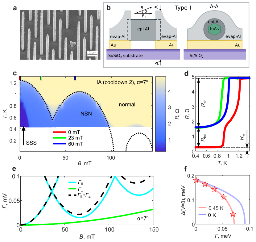
We start from superconducting properties in equilibrium, characterized in type-I devices. Here, ohmic contacts are established directly to the shell, see the sample layout and contact cross-section in Fig. 1b. High quality interface between epitaxial aluminum (epi-Al) and nm thick e-gun evaporated aluminum (evap-Al) is achieved via in-situ Ar milling. Fig. 1c is a color-scale plot of the linear response resistance () in device IA as a function of and (cooldown 2). Three regimes are identified: normal high- regime, superconducting low- and low- regime (SSS) and intermediate regime with the superconducting shell and normal contacts (NSN). The regimes change at the transitions of the epi-Al and evap-Al from the normal to the superconducting state, with representative curves displayed in Fig. 1d. In = (red line) exhibits two steps at the critical temperatures () of the epi-Al (K) and evap-Al (K). In the latter case, the reduced is a result of inverse proximity effect from the Au layer. At lower the resistance saturates at , which we attribute to the wiring contribution. Two other traces taken above the critical -field of the evap-Al show only a single step on the at the of the epi-Al. This data gives the resistances of evap-Al/epi-Al interfaces and of the epi-Al shell . As shown in the SM, a series contribution of the contact pads in is negligible.
The of the epi-Al in Fig. 1c exhibits the Little-Parks (LP) oscillations in the -field, which enables to extract microscopic parameters of the shell. The dependence of is controlled by the depairing factor , which has contributions from parallel () and perpendicular () components of the -field. Here is a small angle between the NW axis and the -field, which is not controlled in the experiment and treated as a fit parameter, separately in each device and in each cooldown. In our calculations we closely follow the Usadel theory in the formalism of Ref. [61], see the SM for the details. The is found from the Abrikosov-Gorkov equation [42, 59] (dotted line in Fig. 1c). is derived in the approximation of a cylindrical shell with the inner radius of and thickness of , without the assumption that . The best fits provide =804 nm, =42 nm and diffusion coefficient =69 . The order parameter and the superconducting coherence length in the limit of =, = are obtained from the BCS relation . The calculated dependencies in device IA (cooldown 2) in different LP lobes and for = and =0 are plotted, respectively, in Figs. 1e and 1f.
Next we investigate the fate of shell superconductivity in response to transport current (). Here, three different scenarios can be expected. In devices with superconducting reservoirs directly contacting the shell, the superconductivity breaks down in a conventional way at the shell critical current . This is realized in type-I devices in the SSS regime. In devices with normal reservoirs, the resistance is always finite and quasiparticle non-equilibrium plays crucial role [43]. The electronic energy distribution (EED, ) is then determined by a competition of finite and energy relaxation. Without relaxation, is a non-equilibrium double-step , where is the Fermi-Dirac EED at a given . This EED implies symmetric coupling to the reservoirs [43, 44], that agrees with the experimental data. For strong relaxation, local equilibrium is achieved with , where is the electronic temperature in the island. In the first case the superconductivity is destroyed at a critical voltage [43, 44, 48, 57] , whereas in the second case it collapses at =. The two limiting cases are realized, respectively, in type-I and type-II devices.
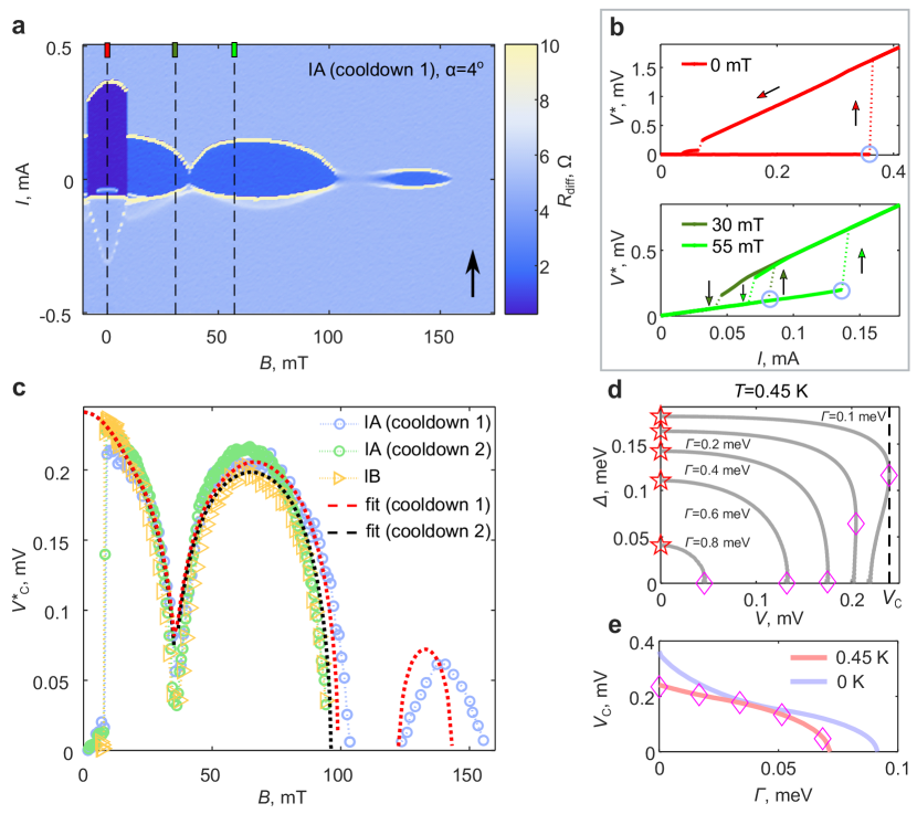
Fig. 2 summarizes the non-equilibrium response in type-I device IA (cooldown 1). Fig. 2a is a color-scale plot of the differential resistance at = in dependence on and , with the current sweep direction indicated by the arrow. Here, is the actual bias on the device with subtracted wiring contribution. Vertical dashed lines correspond to - curves displayed in Fig. 2b for both sweep directions. A superconducting behavior with is found in the SSS regime (upper panel), whereas finite-resistance superconductivity is evident in the NSN regime (lower panel). In both cases, the usual huge hysteresis is found [48]. We are interested in a suppression of the superconducting state, which occurs at increasing and is manifested by a single jump on the - curves. Critical voltages measured right before this jump are exemplified by circles in Fig. 2b. Symbols in Fig. 2c display the -field evolution of in device IA (two cooldowns) and in device IB. In the SSS regime, a small residual voltage is measured, possibly originating from phase-slips or vortices in , thus the superconductivity is destroyed in a conventional way at a critical current. The value of mA is a factor of two smaller compared to the thermodynamical critical current of the epi-Al, the difference most likely coming from the interface resistance (see the SM). By contrast, in the NSN regime the superconductivity collapses at smaller and at . The measured is consistent among the devices and cooldowns, with deviations at higher -fields caused by variations of .
We explain the evolution of in the NSN regime by the Usadel theory, taking into account the non-equilibrium EED in spirit of Ref. [43]. We find the solution in the depth of the S-island, at distances larger than from the ends, where the charge-imbalance decays and the non-equilibrium EED is of the form . Self-consistent numerical procedure to find is detailed in the SM. Fig. 2d shows the results for a set of (solid lines). Data in equilibrium (=) is the same as in Fig. 1f (stars). At increasing , gets suppressed, so that no solution exists above certain (diamonds, dashed line). At small the solution is bistable just below , consistent with previous results [43, 44, 48, 57]. Calculated is shown in Fig. 2e along with the symbols from Fig. 2d. Using the - correspondence the dependencies are obtained and plotted in Fig. 2c for the device IA in two cooldowns (dashed lines). Near perfect agreement with the experiment ensures that the relaxation-free scenario of non-equilibrium superconductivity is realized in type-I devices.
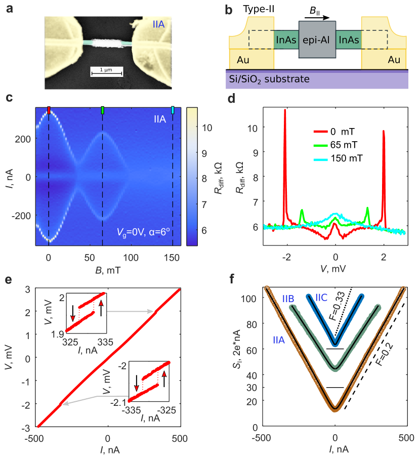
We now switch to type-II devices, where the selectively etched shell forms a floating S-island of the length , see the micrograph and sketch in Figs. 3a and 3b. Ohmic contacts are defined via evaporation of Cr/Au with ex-situ passivation of the native oxide in ammonium polysulfide [62, 25, 6]. Thanks to the InAs segments, the device resistance is about four orders of magnitude higher than in type-I devices and is controllable by the back gate voltage . Figs. 3c and 3d show, respectively, the color-scale plot in device IIA and representative traces at fixed , corresponding to vertical dashed lines in the color-plot. Low bias behavior of is a combination of the superconducting proximity effect in diffusive NS junctions with non-ideal interface [7, 15, 18], observable at low -fields, and Coulomb effects [63, 64, 65], which contribute a broad zero-bias resistance maximum, observable at high -fields. We do not discuss these device specific and -dependent properties and concentrate on a sharp resistance peak observed in all devices at much higher . The LP oscillations of the peak position (Fig. 3c), and the tiny voltage jump the peak originates from (Fig. 3e), show that this feature is associated with the collapse of superconductivity. Corresponding voltage jumps are most pronounced at = and demonstrate weak hysteresis, see the insets of Fig. 3e. At increasing they smear out and the visibility of the LP oscillations reduces (Fig. 3c).
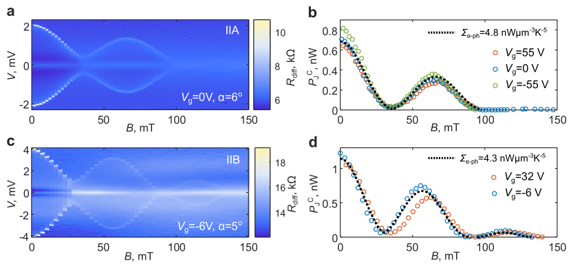
The observation of superconducting state at voltages implies strong energy relaxation. Otherwise, as found in type-I devices, the double-step EED in the S-island would not be compatible with the superconductivity. Although in the type-II devices a moderate asymmetry of the couplings to the reservoirs can affect the EED and reduce the effect of non-equilibrium [44, 57], it is too weak to maintain the superconducting state at mV-range biases. A direct test of the relaxation is achieved via shot noise measurements in the normal state, shown in Fig. 3f, see SM for the details. The noise spectral density (symbols) exhibits a shot noise behavior with Fano factors (dashed line). This value is considerably reduced compared to the universal in diffusive conductors without relaxation [66, 67], usually found in InAs NWs [68, 69, 18] (dotted line). The reduction of is a result of strong e-ph relaxation in the S-island [70]. We assume local equilibrium EED with the electronic temperature, which obeys the heat balance equation . Here, is the Joule power, half of which is dissipated in the S-island, is the volume of the epi-Al and is the e-ph cooling power. Note a conceptual difference from Ref. [59], in which the Joule power flows into the reservoirs by the electronic heat conduction. The above equation simultaneously explains the shot noise in Fig. 3f (solid lines) and the suppression of superconductivity by transport current. In the latter case, the superconductivity collapses at the critical Joule power (), which corresponds to =. The dependencies in devices IIA and IIB are shown in Figs. 4b and 4d (symbols) and correspond, respectively, to the color-plots in Figs. 4a and 4c. We fit the data in these and other devices with similar , see the dashed lines (more data in the SM). This value corresponds to the e-ph relaxation time of ns at =, in agreement with independent measurements in aluminum [71]. The weak dependence of observed in several devices indicates minor deviations from local equilibrium.
The origin of different behavior in type-I and type-II devices is in the ratio of quasiparticle dwell time in the S-island , controlled by the coupling to the reservoirs, and . Type-I devices are strongly coupled to reservoirs and the dwell time is mainly limited by diffusion ns for the typical . In type-II devices is smaller, however, the coupling to reservoirs is very weak owing to highly resistive InAs segments. Thus, the dwell time is renormalized by the ratio of the numbers of the eigenmodes in epi-Al and in InAs or, roughly, by the ratio of semiconductor and superconductor resistances in the normal state (), giving . The relation naturally explains the relaxation-free regime in type-I devices and strong relaxation regime in type-II devices. Note that these estimates strongly depend on the bath temperature, since , meaning that intermediate regime is expected at lower in type-II devices.
In summary, our results illuminate the way in which the superconducting order parameter and the bias and relaxation controlled quasiparticle population are bound with each other in floating S-islands in semi-super hybrids. This binding indicates a general shortcoming of the transport spectroscopy in such devices, since the excitation spectrum of a mesoscopic hybrid device becomes dependent on the bias voltage and relaxation.
We acknowledge valuable advices of Ya.V. Fominov and A.S. Mel’nikov on the Usadel theory and fabrication help of S.V. Egorov. We thank A.V. Bubis for his input on the early stages of this work and for useful remarks. VSK is grateful to T.M. Klapwijk for the early illuminating discussions of non-equilibrium superconductivity. The work was supported by the Russian Science Foundation project 22-12-00342.
References
- Lutchyn et al. [2010] R. M. Lutchyn, J. D. Sau, and S. Das Sarma, Majorana Fermions and a Topological Phase Transition in Semiconductor-Superconductor Heterostructures, Physical Review Letters 105, 077001 (2010).
- Oreg et al. [2010] Y. Oreg, G. Refael, and F. Von Oppen, Helical Liquids and Majorana Bound States in Quantum Wires, Physical Review Letters 105, 177002 (2010).
- Prada et al. [2020] E. Prada, P. San-Jose, M. W. A. De Moor, A. Geresdi, E. J. H. Lee, J. Klinovaja, D. Loss, J. Nygård, R. Aguado, and L. P. Kouwenhoven, From Andreev to Majorana bound states in hybrid superconductor–semiconductor nanowires, Nature Reviews Physics 2, 575 (2020).
- Chang et al. [2015] W. Chang, S. M. Albrecht, T. S. Jespersen, F. Kuemmeth, P. Krogstrup, J. Nygård, and C. M. Marcus, Hard gap in epitaxial semiconductor–superconductor nanowires, Nature Nanotechnology 10, 232 (2015).
- Krogstrup et al. [2015] P. Krogstrup, N. L. B. Ziino, W. Chang, S. M. Albrecht, M. H. Madsen, E. Johnson, J. Nygård, C. M. Marcus, and T. S. Jespersen, Epitaxy of semiconductor–superconductor nanowires, Nature Materials 14, 400 (2015).
- Gül et al. [2017] Ö. Gül, H. Zhang, F. K. de Vries, J. van Veen, K. Zuo, V. Mourik, S. Conesa-Boj, M. P. Nowak, D. J. van Woerkom, M. Quintero-Pérez, M. C. Cassidy, A. Geresdi, S. Koelling, D. Car, S. R. Plissard, E. P. A. M. Bakkers, and L. P. Kouwenhoven, Hard superconducting gap in InSb nanowires, Nano Letters 17, 2690 (2017).
- Bubis [2017] A. V. Bubis, Proximity effect and interface transparency in Al/InAs-nanowire/Al diffusive junctions, Semicond. Sci. Technol. 32, 094007 (2017).
- Jünger et al. [2020] C. Jünger, R. Delagrange, D. Chevallier, S. Lehmann, K. A. Dick, C. Thelander, J. Klinovaja, D. Loss, A. Baumgartner, and C. Schönenberger, Magnetic-Field-Independent Subgap States in Hybrid Rashba Nanowires, Physical Review Letters 125, 017701 (2020).
- Yu et al. [2023] P. Yu, B. D. Woods, J. Chen, G. Badawy, E. P. A. M. Bakkers, T. D. Stanescu, and S. M. Frolov, Delocalized states in three-terminal superconductor-semiconductor nanowire devices, SciPost Physics 15, 005 (2023).
- Jünger et al. [2019] C. Jünger, A. Baumgartner, R. Delagrange, D. Chevallier, S. Lehmann, M. Nilsson, K. A. Dick, C. Thelander, and C. Schönenberger, Spectroscopy of the superconducting proximity effect in nanowires using integrated quantum dots, Communications Physics 2, 76 (2019).
- Stanescu and Tewari [2014] T. D. Stanescu and S. Tewari, Nonlocality of zero-bias anomalies in the topologically trivial phase of Majorana wires, Physical Review B 89, 220507 (2014).
- Rosdahl et al. [2018] T. Ö. Rosdahl, A. Vuik, M. Kjaergaard, and A. R. Akhmerov, Andreev rectifier: A nonlocal conductance signature of topological phase transitions, Physical Review B 97, 045421 (2018).
- Lai et al. [2019] Y.-H. Lai, J. D. Sau, and S. Das Sarma, Presence versus absence of end-to-end nonlocal conductance correlations in Majorana nanowires: Majorana bound states versus Andreev bound states, Physical Review B 100, 045302 (2019).
- Ménard et al. [2020] G. C. Ménard, G. L. R. Anselmetti, E. A. Martinez, D. Puglia, F. K. Malinowski, J. S. Lee, S. Choi, M. Pendharkar, C. J. Palmstrøm, K. Flensberg, C. M. Marcus, L. Casparis, and A. P. Higginbotham, Conductance-Matrix Symmetries of a Three-Terminal Hybrid Device, Physical Review Letters 124, 036802 (2020).
- Denisov et al. [2021] A. O. Denisov, A. V. Bubis, S. U. Piatrusha, N. A. Titova, A. G. Nasibulin, J. Becker, J. Treu, D. Ruhstorfer, G. Koblmüller, E. S. Tikhonov, and V. S. Khrapai, Charge-neutral nonlocal response in superconductor-InAs nanowire hybrid devices, Semicond. Sci. Technol. 36, 09LT04 (2021).
- Puglia et al. [2021] D. Puglia, E. A. Martinez, G. C. Ménard, A. Pöschl, S. Gronin, G. C. Gardner, R. Kallaher, M. J. Manfra, C. M. Marcus, A. P. Higginbotham, and L. Casparis, Closing of the Induced Gap in a Hybrid Superconductor-Semiconductor Nanowire, Physical Review B 103, 235201 (2021).
- Pan et al. [2021] H. Pan, J. D. Sau, and S. Das Sarma, Three-terminal nonlocal conductance in Majorana nanowires: Distinguishing topological and trivial in realistic systems with disorder and inhomogeneous potential, Physical Review B 103, 014513 (2021).
- Denisov et al. [2022] A. Denisov, A. Bubis, S. Piatrusha, N. Titova, A. Nasibulin, J. Becker, J. Treu, D. Ruhstorfer, G. Koblmüller, E. Tikhonov, and V. Khrapai, Heat-Mode Excitation in a Proximity Superconductor, Nanomaterials 12, 1461 (2022).
- Wang et al. [2022a] G. Wang, T. Dvir, N. Van Loo, G. P. Mazur, S. Gazibegovic, G. Badawy, E. P. A. M. Bakkers, L. P. Kouwenhoven, and G. De Lange, Nonlocal measurement of quasiparticle charge and energy relaxation in proximitized semiconductor nanowires using quantum dots, Physical Review B 106, 064503 (2022a).
- Kejriwal and Muralidharan [2022] A. Kejriwal and B. Muralidharan, Nonlocal conductance and the detection of Majorana zero modes: Insights from von Neumann entropy, Physical Review B 105, L161403 (2022).
- Akhmerov et al. [2011] A. R. Akhmerov, J. P. Dahlhaus, F. Hassler, M. Wimmer, and C. W. J. Beenakker, Quantized Conductance at the Majorana Phase Transition in a Disordered Superconducting Wire, Physical Review Letters 106, 057001 (2011).
- Nishio et al. [2011] T. Nishio, T. Kozakai, S. Amaha, M. Larsson, H. A. Nilsson, H. Q. Xu, G. Zhang, K. Tateno, H. Takayanagi, and K. Ishibashi, Supercurrent through InAs nanowires with highly transparent superconducting contacts, Nanotechnology 22, 445701 (2011).
- Abay et al. [2012] S. Abay, H. Nilsson, F. Wu, H. Xu, C. Wilson, and P. Delsing, High Critical-Current Superconductor-InAs Nanowire-Superconductor Junctions, Nano Letters 12, 5622 (2012).
- Abay et al. [2014] S. Abay, D. Persson, H. Nilsson, F. Wu, H. Q. Xu, M. Fogelström, V. Shumeiko, and P. Delsing, Charge transport in InAs nanowire Josephson junctions, Physical Review B 89, 214508 (2014).
- Paajaste et al. [2015] J. Paajaste, M. Amado, S. Roddaro, F. S. Bergeret, D. Ercolani, L. Sorba, and F. Giazotto, Pb/InAs Nanowire Josephson Junction with High Critical Current and Magnetic Flux Focusing, Nano Letters 15, 1803 (2015).
- Perla [2021] P. Perla, Fully in situ Nb/InAs-nanowire Josephson junctions by selective-area growth and shadow evaporation, Nanoscale Advances 3, 1413 (2021).
- Kousar et al. [2022] B. Kousar, D. J. Carrad, L. Stampfer, P. Krogstrup, J. Nygård, and T. S. Jespersen, InAs/MoRe Hybrid Semiconductor/Superconductor Nanowire Devices, Nano Letters 22, 8845 (2022).
- Spanton et al. [2017] E. M. Spanton, M. Deng, S. Vaitiekėnas, P. Krogstrup, J. Nygård, C. M. Marcus, and K. A. Moler, Current–phase relations of few-mode InAs nanowire Josephson junctions, Nature Physics 13, 1177 (2017).
- Hart [2019] S. Hart, Current-phase relations of InAs nanowire Josephson junctions: From interacting to multimode regimes, Physical Review B 100, 064523 (2019).
- Das et al. [2012a] A. Das, Y. Ronen, Y. Most, Y. Oreg, M. Heiblum, and H. Shtrikman, Zero-bias peaks and splitting in an Al–InAs nanowire topological superconductor as a signature of Majorana fermions, Nature Physics 8, 887 (2012a).
- Mourik et al. [2012] V. Mourik, K. Zuo, S. M. Frolov, S. R. Plissard, E. P. A. M. Bakkers, and L. P. Kouwenhoven, Signatures of Majorana Fermions in Hybrid Superconductor-Semiconductor Nanowire Devices, Science 336, 1003 (2012).
- Vaitiekėnas et al. [2020a] S. Vaitiekėnas, G. W. Winkler, B. Van Heck, T. Karzig, M.-T. Deng, K. Flensberg, L. I. Glazman, C. Nayak, P. Krogstrup, R. M. Lutchyn, and C. M. Marcus, Flux-induced topological superconductivity in full-shell nanowires, Science 367, eaav3392 (2020a).
- Vaitiekėnas et al. [2021] S. Vaitiekėnas, Y. Liu, P. Krogstrup, and C. M. Marcus, Zero-bias peaks at zero magnetic field in ferromagnetic hybrid nanowires, Nature Physics 17, 43 (2021).
- Valentini et al. [2021] M. Valentini, F. Peñaranda, A. Hofmann, M. Brauns, R. Hauschild, P. Krogstrup, P. San-Jose, E. Prada, R. Aguado, and G. Katsaros, Nontopological zero-bias peaks in full-shell nanowires induced by flux-tunable Andreev states, Science 373, 82 (2021).
- Hofstetter et al. [2009] L. Hofstetter, S. Csonka, J. Nygård, and C. Schönenberger, Cooper pair splitter realized in a two-quantum-dot Y-junction, Nature 461, 960 (2009).
- Herrmann et al. [2010] L. G. Herrmann, F. Portier, P. Roche, A. L. Yeyati, T. Kontos, and C. Strunk, Carbon Nanotubes as Cooper-Pair Beam Splitters, Physical Review Letters 104, 026801 (2010).
- Das et al. [2012b] A. Das, Y. Ronen, M. Heiblum, D. Mahalu, A. V. Kretinin, and H. Shtrikman, High-efficiency Cooper pair splitting demonstrated by two-particle conductance resonance and positive noise cross-correlation, Nature Communications 3, 1165 (2012b).
- Baba et al. [2018] S. Baba, C. Jünger, S. Matsuo, A. Baumgartner, Y. Sato, H. Kamata, K. Li, S. Jeppesen, L. Samuelson, H. Xu, C. Schönenberger, and S. Tarucha, Cooper-pair splitting in two parallel InAs nanowires, New Journal of Physics 20, 063021 (2018).
- Wang et al. [2022b] G. Wang, T. Dvir, G. P. Mazur, C.-X. Liu, N. Van Loo, S. L. D. Ten Haaf, A. Bordin, S. Gazibegovic, G. Badawy, E. P. A. M. Bakkers, M. Wimmer, and L. P. Kouwenhoven, Singlet and triplet Cooper pair splitting in hybrid superconducting nanowires, Nature 612, 448 (2022b).
- Bordoloi et al. [2022] A. Bordoloi, V. Zannier, L. Sorba, C. Schönenberger, and A. Baumgartner, Spin cross-correlation experiments in an electron entangler, Nature 612, 454 (2022).
- Scherübl et al. [2022] Z. Scherübl, G. Fülöp, J. Gramich, A. Pályi, C. Schönenberger, J. Nygård, and S. Csonka, From Cooper pair splitting to the non-local spectroscopy of a Shiba state, Physical Review Research 4, 023143 (2022).
- Vaitiekėnas et al. [2020b] S. Vaitiekėnas, P. Krogstrup, and C. M. Marcus, Anomalous metallic phase in tunable destructive superconductors, Physical Review B 101, 060507 (2020b).
- Keizer et al. [2006] R. S. Keizer, M. G. Flokstra, J. Aarts, and T. M. Klapwijk, Critical Voltage of a Mesoscopic Superconductor, Physical Review Letters 96, 147002 (2006).
- Snyman and Nazarov [2009] I. Snyman and Yu. V. Nazarov, Bistability in voltage-biased normal-metal/insulator/superconductor/insulator/normal-metal structures, Physical Review B 79, 014510 (2009).
- Huard et al. [2007] B. Huard, H. Pothier, D. Esteve, and K. E. Nagaev, Electron heating in metallic resistors at sub-Kelvin temperature, Physical Review B 76, 165426 (2007).
- Sivre et al. [2018] E. Sivre, A. Anthore, F. D. Parmentier, A. Cavanna, U. Gennser, A. Ouerghi, Y. Jin, and F. Pierre, Heat Coulomb blockade of one ballistic channel, Nature Physics 14, 145 (2018).
- Rosenblatt et al. [2020] A. Rosenblatt, S. Konyzheva, F. Lafont, N. Schiller, J. Park, K. Snizhko, M. Heiblum, Y. Oreg, and V. Umansky, Energy Relaxation in Edge Modes in the Quantum Hall Effect, Physical Review Letters 125, 256803 (2020).
- Vercruyssen et al. [2012] N. Vercruyssen, T. G. A. Verhagen, M. G. Flokstra, J. P. Pekola, and T. M. Klapwijk, Evanescent states and nonequilibrium in driven superconducting nanowires, Physical Review B 85, 224503 (2012).
- Fu [2010] L. Fu, Electron Teleportation via Majorana Bound States in a Mesoscopic Superconductor, Physical Review Letters 104, 056402 (2010).
- Ulrich and Hassler [2015] J. Ulrich and F. Hassler, Majorana-assisted nonlocal electron transport through a floating topological superconductor, Physical Review B 92, 075443 (2015).
- Albrecht et al. [2016] S. M. Albrecht, A. P. Higginbotham, M. Madsen, F. Kuemmeth, T. S. Jespersen, J. Nygård, P. Krogstrup, and C. M. Marcus, Exponential protection of zero modes in Majorana islands, Nature 531, 206 (2016).
- Lai et al. [2021] Y.-H. Lai, S. D. Sarma, and J. D. Sau, Theory of Coulomb blockaded transport in realistic Majorana nanowires, Physical Review B 104, 085403 (2021).
- Hao et al. [2022] Y. Hao, G. Zhang, D. Liu, and D. E. Liu, Double Fu-teleportation and anomalous Coulomb blockade in a Majorana-hosted superconducting island, Nature Communications 13, 6699 (2022).
- Souto et al. [2022] R. S. Souto, M. M. Wauters, K. Flensberg, M. Leijnse, and M. Burrello, Multiterminal transport spectroscopy of subgap states in Coulomb-blockaded superconductors, Physical Review B 106, 235425 (2022).
- Valentini et al. [2022] M. Valentini, M. Borovkov, E. Prada, S. Martí-Sánchez, M. Botifoll, A. Hofmann, J. Arbiol, R. Aguado, P. San-Jose, and G. Katsaros, Majorana-like Coulomb spectroscopy in the absence of zero-bias peaks, Nature 612, 442 (2022).
- Roddaro et al. [2011] S. Roddaro, A. Pescaglini, D. Ercolani, L. Sorba, F. Giazotto, and F. Beltram, Hot-electron effects in InAs nanowire Josephson junctions, Nano Research 4, 259 (2011).
- Bubis [2021] A. V. Bubis, Thermal conductance and nonequilibrium superconductivity in a diffusive NSN wire probed by shot noise, Physical Review B 104, 125409 (2021).
- Liu et al. [2023] M.-L. Liu, D. Pan, T. Le, J.-B. He, Z.-M. Jia, S. Zhu, G. Yang, Z.-Z. Lyu, G.-T. Liu, J. Shen, J.-H. Zhao, L. Lu, and F.-M. Qu, Gate-Tunable Negative Differential Conductance in Hybrid Semiconductor–Superconductor Devices, Chinese Physics Letters 40, 067301 (2023).
- Ibabe et al. [2023] A. Ibabe, M. Gómez, G. O. Steffensen, T. Kanne, J. Nygård, A. L. Yeyati, and E. J. H. Lee, Joule spectroscopy of hybrid superconductor–semiconductor nanodevices, Nature Communications 14, 2873 (2023).
- [60] See the Supplemental Materials file at [URL], which includes Refs. [72-75].
- Anthore et al. [2003] A. Anthore, H. Pothier, and D. Esteve, Density of States in a Superconductor Carrying a Supercurrent, Physical Review Letters 90, 127001 (2003).
- Sourribes et al. [2013] M. J. L. Sourribes, I. Isakov, M. Panfilova, and P. A. Warburton, Minimization of the contact resistance between InAs nanowires and metallic contacts, Nanotechnology 24, 045703 (2013).
- Nazarov [1999] Y. V. Nazarov, Coulomb Blockade without Tunnel Junctions, Physical Review Letters 82, 1245 (1999).
- Golubev and Zaikin [2001] D. S. Golubev and A. D. Zaikin, Coulomb Interaction and Quantum Transport through a Coherent Scatterer, Physical Review Letters 86, 4887 (2001).
- Yeyati et al. [2001] A. L. Yeyati, A. Martin-Rodero, D. Esteve, and C. Urbina, Direct Link between Coulomb Blockade and Shot Noise in a Quantum-Coherent Structure, Physical Review Letters 87, 046802 (2001).
- Nagaev [1992] K. Nagaev, On the shot noise in dirty metal contacts, Physics Letters A 169, 103 (1992).
- Beenakker and Buttiker [1992] C. W. J. Beenakker and M. Buttiker, Suppression of shot noise in metallic diffusive conductors, Physical Review B 46, 1889 (1992).
- E S Tikhonov et al. [2016] E S Tikhonov, D V Shovkun, D Ercolani, F Rossella, M Rocci, L Sorba, S Roddaro, and V S Khrapai, Local noise in a diffusive conductor, Scientific Reports 6, 30621 (2016).
- Tikhonov [2016] E. S. Tikhonov, Noise thermometry applied to thermoelectric measurements in InAs nanowires, Semicond. Sci. Technol. 31, 104001 (2016).
- De Jong and Beenakker [1996] M. De Jong and C. Beenakker, Semiclassical theory of shot noise in mesoscopic conductors, Physica A: Statistical Mechanics and its Applications 230, 219 (1996).
- Pinsolle et al. [2016] E. Pinsolle, A. Rousseau, C. Lupien, and B. Reulet, Direct measurement of the electron energy relaxation dynamics in metallic wires, Physical Review Letters 116, 236601 (2016).
- Ruhstorfer et al. [2021] D. Ruhstorfer, A. Lang, S. Matich, M. Döblinger, H. Riedl, J. J. Finley, and G. Koblmüller, Growth dynamics and compositional structure in periodic InAsSb nanowire arrays on Si (111) grown by selective area molecular beam epitaxy, Nanotechnology 32, 135604 (2021).
- Del Giudice et al. [2020] F. Del Giudice, J. Becker, C. De Rose, M. Döblinger, D. Ruhstorfer, L. Suomenniemi, J. Treu, H. Riedl, J. J. Finley, and G. Koblmüller, Ultrathin catalyst-free InAs nanowires on silicon with distinct 1D sub-band transport properties, Nanoscale 12, 21857 (2020).
- Rudolph et al. [2013] D. Rudolph, S. Funk, M. Döblinger, S. Morkötter, S. Hertenberger, L. Schweickert, J. Becker, S. Matich, M. Bichler, D. Spirkoska, I. Zardo, J. J. Finley, G. Abstreiter, and G. Koblmüller, Spontaneous Alloy Composition Ordering in GaAs-AlGaAs Core–Shell Nanowires, Nano Letters 13, 1522 (2013).
- Tikhonov et al. [2014] E. S. Tikhonov, M. Yu. Melnikov, D. V. Shovkun, L. Sorba, G. Biasiol, and V. S. Khrapai, Nonlinear transport and noise thermometry in quasiclassical ballistic point contacts, Physical Review B 90, 161405 (2014).