Characterization of FBK “NUV-HD-Cryo” SiPMs at 10 K
Abstract
We report the characterization of the FBK “NUV-HD-Cryo” SiPMs at 10 K temperature. With 405 nm and 530 nm light, we measured the photo-detection efficiency (PDE) at the bias voltages between 6 to 11 V overvoltage (OV). The PDE reaches 40% for 405 nm and 530 nm light with a bias voltage of OV 9 V. A bias voltage higher than 9 V leads to a slightly greater PDE. We also measured the SiPMs’ PDE at room temperature (RT). The results are consistent with the measurements on the similar model SiPMs by other groups. The I-V curve of the SiPMs differs significantly from the conventional one measured at RT. The dark current ratio (DCR) is tested to be 1 Hz for the 92 mm2 SiPMs, or 0.01 Hz/mm2, which is 7 orders lower than the ratio tested at RT. The SiPMs’ performance at 10 K demonstrated that it could be equipped on a liquid helium detector as the photosensor to search for rare events, including but not limited to dark matter searches.
I Introduction
With different configurations, liquid helium (LHe) detectors have been proposed or implemented to search for Solar neutrinos [1, 2, 3], dark matter [4, 5, 6, 7, 8, 9, 10], and neutron electron dipole moment (nEDM) [11, 12, 13, 14, 15]. Many of these detectors record the scintillation produced by incident particles and background particles. Silicon photomultipliers (SiPMs) might be the best choice of photosensors to detect the visible light shifted from LHe’s 80 nm scintillation with a wavelength shifter. In principle, photomultipliers (PMTs) could be another possible option. However, they might not be suitable for long-term running because helium gas can permeate through the glass and into the vacuum space of the photosensor. If that happens, an increase in dark current and degradation of the breakdown voltage is foreseen; even worse, the PMTs performance will deteriorate or cannot work anymore since a discharge could happen inside the tube [16].
The paper will be organized as follows. In section II, we mainly introduce the photon detection efficiency (PDE) tests of a specific type of Fondazione Bruno Kessler (FBK) SiPMs at 10 K. We then continue to discuss the dark current ratio (DCR) measurement in section III. We have discussions and summaries in section IV.
II The PDE tests at 10 K
As a dark matter detector aiming to hunt for low-mass WIMPs down to sub-GeV/c2 WIMPs, a liquid helium (LHe) time projection chamber (TPC) should be equipped with photosensors having a PDE greater than 40%, as discussed in our previous publication [9]. For the FBK SiPMs we are planning to use, the PDE has been measured at room temperature (RT) to be greater than 40% with the bias voltage of 5 V overvoltage (OV)[18, 19]. However, according to our communications with the FBK company, no group has measured the photosensor’ PDE at LHe temperature yet [20]. Compared to calibrating a SiPMs’ PDE at RT, as demonstrated in references [21, 22, 23, 24, 25, 18], the same calibration at LHe temperature requires two additional preconditions. (a) A cryogenic facility is needed to cool the SiPMs down, and (b) the responsivity of a photodiode (an essential part for a PDE test; see below for more details) must be calibrated around 4 K. Our original plan was to calibrate the diode at the National Institute of Standards and Technology (NIST). However, we have been told that they can not do the calibration for the moment, though they are supposed to be capable of doing that in the future [26]. Luckily, we have a Gifford-McMahon (G-M) cryocooler at the China Institute of Atomic Energy (CIAE) to cool the SiPMs; and even more lucky, a group at the National Institute of Metrology (NIM) in China kindly agreed to calibrate our photodiode’s responsivity in their G-M cryocooler as a side-project of their primary research programs. However, they can only calibrate two wavelengths, 405 and 530 nm; fortunately, they are within the wavelength of TPB (Tetra-Phenyl-Butadiene)-shifted LHe scintillation, 350 - 600 nm [27].
II.1 PDE tests setup
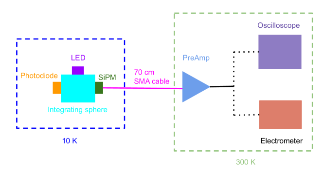
As mentioned in references [23, 18, 28], the PDE can be obtained by measuring the relative efficiency between the to-be-tested SiPMs and a calibrated photodiode. To read a SiPMs’ signal at LHe temperature, one has to decide where the readout system, especially the preamplifier, should be located first. Reference [29] used a cryogenic preamplifier capable of working at 40 K. High electron mobility transistors (HEMTs) have been implemented as a preamplifier at 4 K and 10 mK [30, 31]. While other references [32, 33] put the preamplifier at RT. Since we can not get a preamplifier capable of working at LHe temperature, we decided to leave the preamp and the related DAQ system at RT; an LED, a photodiode, and a SiPMs are all in cryogenic; a 70 cm SMA cable connects the SiPMs in cold and the preamplifier in warm, as schematically shown in Fig. 1. The low-noise preamplifier circuit is based on an ultra wide-band, low-power, current feedback operational amplifier (OPA694, TI), which is configured as a non-inverting voltage amplifier with a gain of 46. A low pass RC filter, composed of a 20 serial resistor and a 1 nF capacitor connecting to the ground, is added to the operational amplifier output to further reduce the noise. Depending on the data to take, an 8 GHz bandwidth, 25 GSa/s sample rate digital oscilloscope, or a Keithley 6485 electrometer will be connected.
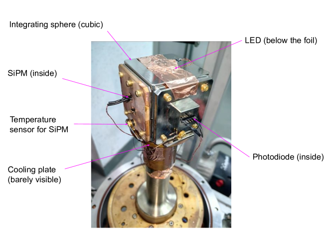
As shown in Fig. 2, the cubic integrating sphere mounts on the (barely visible) cooling plate, which is the cooling source of the cryogenic system. On the surfaces of the sphere, the LED, the photodiode, the SiPMs, and the TS are all fastened. The SiPMs are “NUV-HD-Cryo”, which is provided by the FBK company. The SiPMs have an active window of 11.7 7.9 mm2, with a cell pitch of 30 m. The photodiode is AXUV100G with an active area of 10 10 mm2. Two photodiodes have been calibrated at NIM in China, at 6 K and RT. For more info on the photodiode calibration, please refer to section II.2. We used LEDs to generate 405 nm and 530 nm light. The LEDs can emit monochromatic light with a FWHM typically 5%. The LEDs were driven by hundreds of ns width pulses that were produced by a DG535 111https://www.thinksrs.com/products/dg535.html.
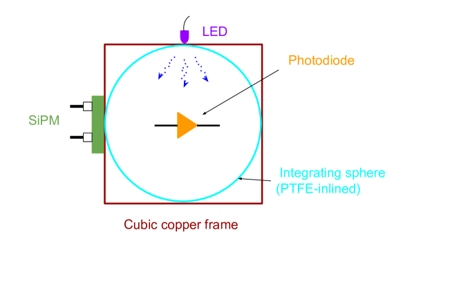
The integrating sphere is designed by us and outsourced to a commercial company in China. The outside of the sphere is cubic, which gives convenience to (a) installing an LED and other parts on the surfaces and (b) mounting itself on the cooling plate of the G-M cryocooler. The inner surface of the 60 mm diameter integrating sphere is coated with highly reflective PTFE. As shown in Fig. 3, The LED, the calibrated photodiode, and the to-be-calibrated SiPMs are 90 degrees from each other. Such a design allows the photodiode and the SiPMs to receive the same ratio of photons as long as the size of the two affiliated ports is fixed without worrying about the intensity profile of light emitted from the LED. In our case, the diameters of the ports for the photodiode and the SiPMs are 4.0 mm and 0.1 mm, respectively.
The G-M cryocooler can approach its lowest temperature after 5 hours of cooling. During our PDE tests, we often run the cooling machine for more than 12 hours prior to a measurement to reach the stable temperature, 10 K. Turning off the cryocooler will increase the SiPMs’ temperature, but it is difficult to keep the photosensor stay at a certain temperature stably, so we only measured the SiPMs PDE at 10 K.
II.2 Photodiode responsivity calibration at NIM in China
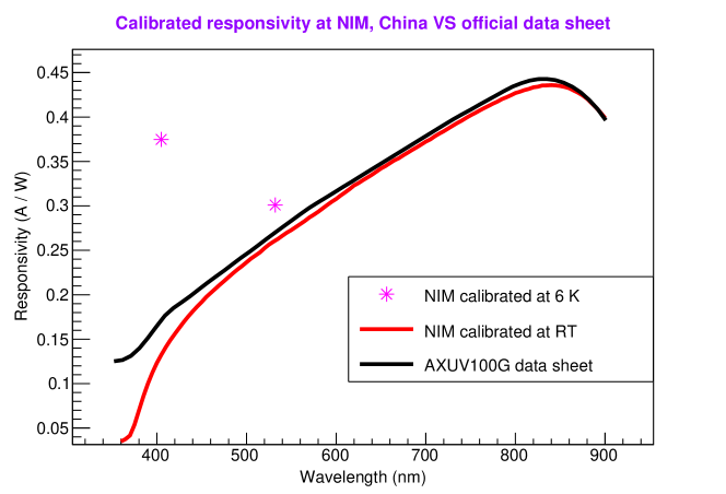
The photodiode under test is AXUV100G from the Opto diode company 222https://optodiode.com. Although the AXUV100G photodiode has a general datasheet on the website, we decided to calibrate our diodes at the National Institute of Metrology (NIM) in China. As shown in Fig. 4, the responsivity calibrated at NIM at RT (the red curve) is consistent with the official data sheet (the black curve). In general, NIM does not calibrate a photodiode at LHe temperature. By coincidence, we knew a team at NIM was calibrating similar photosensors at cryogenic temperature for their research programs, so we asked whether they could calibrate our detector as a favor. They kindly agreed to calibrate two of our photodiodes; each was illuminated with 405 and 532 nm light around 6 K in their G-M cryocooler. The calibrated results are shown in Fig. 4.
During the responsivity calibration at low temperature at NIM, the temperature was measured to be 5.75 K with a sensor having a 1.0 K uncertainty. The sensor and the photodiode were both mounted on the same copper frame and had a distance of about 8.0 cm. Our preliminary COMSOL simulation shows the temperature difference between the photodiode and the temperature sensor is ignorable.
II.3 The I-V curve tests for FBK SiPMs at 10 K
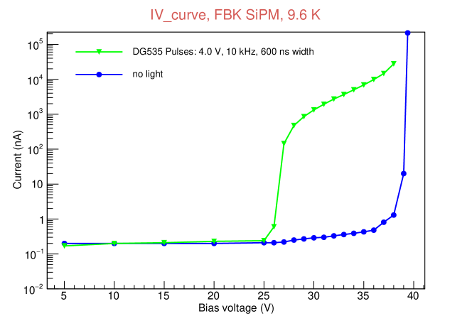
The I-V curves of the SiPMs we measured at RT are consistent with FBK company, as shown in reference [9]. However, at 10 K, we can not observe a typical I-V curve as we have done at RT: the I-V curve appears to be a flat line with a current of nA, as long as the bias voltage reaches a specific value, the current jumps to mA suddenly. The unconventional I-V feature appeared in our 2022 data [9] and this manuscript (the blue curve in Fig. 5). We can not figure out the “abnormal” I-V curve until we have measured the dark current rate (DCR) of the SiPMs. It turned out that due to the especially low DCR at 10 K, 0.01 Hz/mm2, which is 7 orders lower than the DCR at RT, 100 kHz/mm2 [29], the dark current is too small to build up a A current even if the bias voltage is in the breakdown region. As long as the bias voltage continuously increases, the correlated noise increases significantly, which results in the observed mA current.
We tested the I-V curve at 10 K in an alternative way, illuminating the SiPMs with weak pulsed light from an LED, which is driven by a DG535. In this way, we obtained a conventional shape of the I-V curve, as the green curve in Fig. 5 shows. The breakdown voltage of the SiPMs at 10 K is around 26.0 V. In this measurement, the pulses from the DG535 have a height of 4 V, a width of 600 ns, and a frequency of 10 kHz; the wavelength of the LED is 405 nm. So far, we measured four FBK SiPMs with the same method around 10 K, and all of them showed almost the same I-V curves.
II.4 PDE measurements
We implemented the photocurrent method to measure the PDE, as mentioned in reference [18]. The PDE is calculated as equation Eq. (1),
| (1) |
where I and I are the measured current of the SiPMs with light on and off, respectively; G is the gain of the SiPMs; qe is the charge of an electron; ECF stands for Excess Charge Factor, which represents the fake efficiency prompt contributed from cross-talks and after pulses [36, 28]; Ph is the incident photons.
Since a SiPMs’ ECF is supposed to be the same no matter whether it has been illuminated or not, it can also be calculated in a dark environment as long as the bias voltage is the same, as the following,
| (2) |
where I and I are both measured under a dark environment, represent the current when the bias voltage is above or below the breakdown voltage, respectively; the definition of G and qe are the same as Eq. (1); N is the average number of photoelectrons per second in dark condition, which is equivalent to the average number of the Poisson statistical photoelectrons in a test [21, 22, 23, 24, 25, 18].
| (3) |
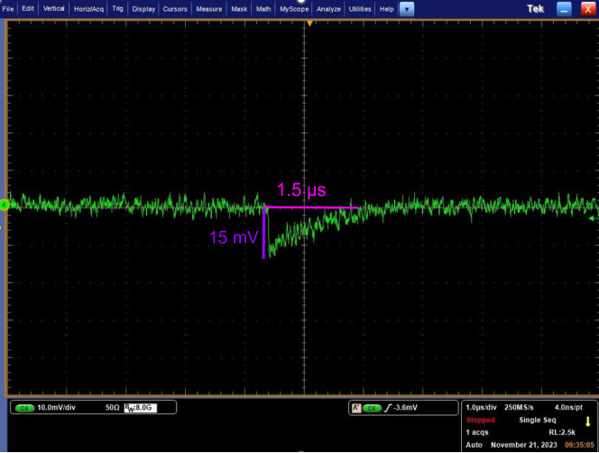
As mentioned above, since the FBK SiPMs’ DCR is only 1 Hz at 10 K with OV = (10 - 12) V, we can not measure a meaningful SiPMs current without light illumination. So, we illuminated the SiPMs with a weak light emitted from an LED driven by a DG535 pulse generator. Whenever the DG535 drove the LED with a pulse, it also sent a trigger to an 8 GHz bandwidth, 25 GSa/s sample rate oscilloscope to record the waveform showing on the screen. A typical single photoelectron (Phe) signal of the FBK SiPMs at 10 K is shown in Fig. 6.
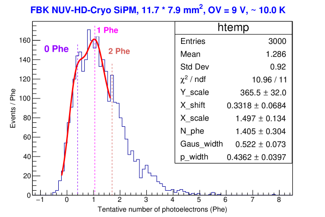
In PDE measurements, the analog signals were first recorded in text files with the oscilloscope and then analyzed offline. Fig. 7 shows a typical charge distribution and a Gaussian convoluted Poisson fit being applied to the histogram. The average number of photoelectrons returned from the fit is 1.405 0.304 Phe, which is the ND to be applied in Eq. (3) for the PDE calculation. For more info on the charge histogram and the fit function, please refer to paper [37]. In the figure, three vertical broken lines indicate the pedestal, one Phe, and 2 Phe peaks, respectively. We intentionally fit only part of the histogram ( 2.0 Phe) to avoid smearing the fit results by the 2+ Phe peaks, many of which are cross-talks and after pulses. In the statistics box, “Y_scale” means the scale factor of the fit function on the Y-axis, “X_scale” indicates the shift on the X-axis, “X_scale” is the scale factor on the X-axis, “N_phe” corresponds to the average number of the Poisson distribution (“”, or the ND under the context), “Gaus_width” and “p_width” are the sigmas of the one Phe and the pedestal peak, respectively.
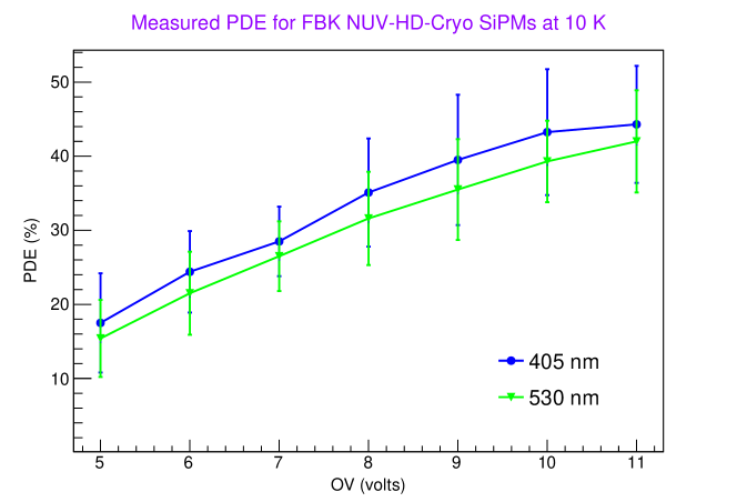
For the SiPMs being applied with OV 9 V bias voltage, illuminated by 405 nm light, and cooled at 10 K, all of the parameters being submitted into Eq. (3) for calculation are shown in table 1. The calculated PDE is ( 39.50 8.77 )%. Following the same procedure, the PDE values measured with other OV and 530 nm light have also been calculated, as shown in Fig. 8.
| ND | ISiPM-L | ISiPM-D | ISiPM | ILeak | PhI | PDE |
| (Phe) | (A) | (nA) | (nA) | (nA) | (photon) | (%) |
| 1.410.30 | 5.300.09 | 0.120.07 | 2.760.02 | 0.020.01 | (6.830.31)E6 | 39.50 8.77 |
II.5 The PDE tests at RT
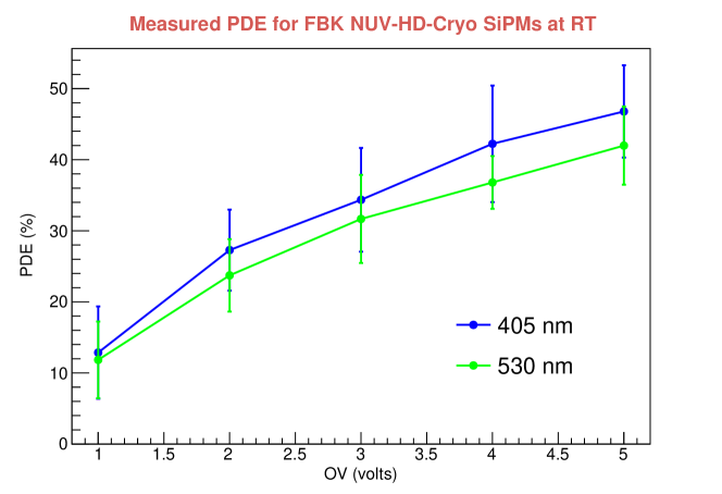
Although our SiPMs are supposed to work at LHe temperatures, we measured the PDE at RT with the similar procedure mentioned above, as shown in Fig. 9. The PDE results are consistent with the measurements on the similar type of FBK SiPMs at RT [19].
III The DCR tests at 10 K
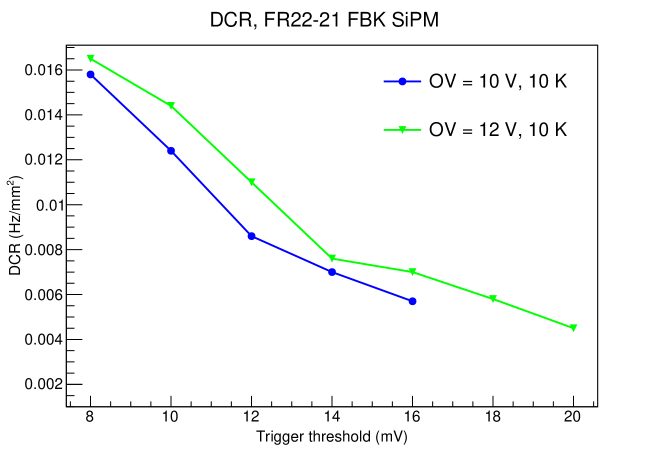
The dark current ratio (DCR) is a critical parameter for a photosensor. Reference [18] measured DCR and other parameters of two types of FBK SiPMs from RT down to 40 K. We need to measure the DCR again because of the following reasons. (a) The SiPMs under our tests are not exactly the same type as the reference according to our discussion with FBK engineers [20]. (b) The working temperature of the SiPMs equipped on an LHe detector would be 4 K, which is significantly lower than 40 K; and according to our experiences of measuring the SiPMs’ I-V curves, the I-V curves are different when the photosensor’s temperatures are below or above 20 K [9], so we suspect the DCR at 10 K might not be the same as 40 K. (c) The dimension of our SiPMs is 11.7 7.9 mm2, which is a factor of six greater than the ones implemented in the reference [18], 4.0 4.0 mm2. As a result, we believe we should measure the SiPMs’ DCR in our G-M cryocooler. We implemented the PDE setup as shown in Fig. 2 for the DCR test. The electronics are slightly different from Fig. 1 , a 5 times amplification amplifier and a counter connected to the preamplifier.
For FBK SiPMs, the typical DCR with 4 to 6 V OV at RT and 40 K are 100 kHz and 0.1 Hz/mm2 (SiPMs specifications: 4 4 mm2, 25 25 m2 NUV-HD-SF) or 0.001 Hz/mm2 (SiPMs specifications: 4 4 mm2, 25 25 m2 NUV-HD-LF) [29], respectively. At 10 K, for the 11.7 7.9 mm2, 30 30 m2 NUV-HD-Cryo type SiPMs, we measured 0.01 Hz/mm2 for OV 10 V and 12 V, as shown in Fig. 10. We believe our results are consistent with the NUV-HD-LF DCR ones tested at 40 K as shown in reference [29] given that (a) the dimension of our SiPMs is six times of the ones tested in the reference, and (b) the OV in our tests are (10 to 12 V), which is 6 volts higher than the (4 to 6 V) in the paper.
IV Summary and discussion
At 10 K, FBK NUV-HD-Cryo SiPMs show significantly different performance than RT according to our tests on the 11.7 7.9 mm2 photosensor. The DCR is only 0.01 Hz/cm2 even with the highest bias voltage, OV = 12 V, which is more than seven orders lower than the one at RT. With an OV 5 V bias voltage, the PDE at 10 K ( 18%) is significantly smaller than at RT ( 45%). However, as long as the bias voltage reaches OV = 9 V, the PDE is greater than 40%, both for 405 or 530 nm light.
TPB-converted scintillation’s wavelength is roughly 350 - 600 nm [27]. Given that the measured PDE at 10 K for 405 nm is about to be 3 % greater than the 530 nm light, as shown in Fig 9, for the PDE of any wavelength between 350 nm and 600 nm, it might be reasonable to extrapolate the efficiency by assuming the PDE changes linearly along with the wavelength, i.e., Eq.( 4),
| (4) |
where PDEN_nm and PDE405_nm are the PDE of a wavelength between 350 - 600 nm and 405 nm, respectively, and can be calculated as Eq. (5),
| (5) |
The uncertainties of the PDE under the two wavelengths are pretty similar to be 8%, and 95% of which is contributed from the average number of photoelectrons in charge fit, ND. A feature of separated photoelectron peaks, such as the 4.0 4.0 mm2 FBK SiPMs measured in reference [18, 19], should be helpful to decrease the error bars significantly. We have tested a 4.0 4.0 mm2 SiPMs at RT with almost the same electronics in our lab and observed distinct peaks. So, the reason that we can not observe separated peaks might be because our SiPMs are 6 times greater than the reference [18, 19].
In summary, we believe our PDE testing results demonstrated that the FBK NUV-HD-Cryo type SIPMs are suitable to be equipped on an LHe TPC, including but not being limited to the ALETHEIA detectors [9].
Acknowledgements.
We gratefully thank the FBK company in Trento, Italy, for providing SiPMs samples; we especially thank Dr. Alberto Gola, Dr. Alberto Mazzi, and Dr. Elena Moretti for helpful discussions and handling logistical work. Particularly, we thank Dr. Elena Moretti for reading our manuscript and addressing insightful comments. In addition, we thank Dr. Wei Hu and Miss. Tangtang Qu at the TOFTech company in Wuxi, Jiangsu, China, for cooperation on electrics development and valuable discussions. We thank Dr. Xiangliang Liu and her team at NIM in China for calibrating two of our photodiodes at 6 K on their facilities for free. We also appreciate Prof. Xiaoguang Wu and Dr. Jinglong Wang at CIAE for their kindness of sharing their DAQ system. Junhui Liao would also thank the support of the “Yuanzhang” funding of CIAE to launch the ALETHEIA program. This work has also been supported by NSFC (National Natural Science Foundation of China) under the contract of 12ED232612001001.References
- Adams et al. [2000] J. Adams, A. Fleischmann, Y. Huang, Y. Kim, R.E.Lanou, H. Maris, and G. Seidel, Progress on heron: A real-time detector for p-p solar neutrinos (2000).
- Adouze and Van [1988] J. Adouze and J. T. T. Van, eds., Proceedings of the Dark Matter in XXIII Rencontres de Moriond (1988).
- HER [1996] Prodeedings of the XXXIst Moriond Conference, Les Arcs, France (1996).
- Guo and McKinsey [2013] W. Guo and D. N. McKinsey, Concept for a dark matter detector using liquid helium-4, Phys. Rev. D 87, 115001 (2013).
- Maris et al. [2017] H. J. Maris, G. M. Seidel, and D. Stein, Dark matter detection using helium evaporation and field ionization, Phys. Rev. Lett. 119, 181303 (2017).
- Hertel et al. [2019a] S. A. Hertel, A. Biekert, J. Lin, V. Velan, and D. N. McKinsey, Direct detection of sub-gev dark matter using a superfluid target, Phys. Rev. D 100, 092007 (2019a).
- Hertel et al. [2019b] S. A. Hertel, A. Biekert, J. Lin, V. Velan, and D. N. McKinsey, Direct detection of sub-gev dark matter using a superfluid target, Phys. Rev. D 100, 092007 (2019b).
- Biekert et al. [2022] A. Biekert, C. Chang, C. W. Fink, M. Garcia-Sciveres, E. C. Glazer, W. Guo, S. A. Hertel, S. Kravitz, J. Lin, M. Lisovenko, R. Mahapatra, D. N. McKinsey, J. S. Nguyen, V. Novosad, W. Page, P. K. Patel, B. Penning, H. D. Pinckney, M. Pyle, R. K. Romani, A. S. Seilnacht, A. Serafin, R. J. Smith, P. Sorensen, B. Suerfu, A. Suzuki, V. Velan, G. Wang, S. L. Watkins, V. G. Yefremenko, L. Yuan, and J. Zhang (SPICE/HeRALD Collaboration), Scintillation yield from electronic and nuclear recoils in superfluid , Phys. Rev. D 105, 092005 (2022).
- Liao et al. [2023] J. Liao, Y. Gao, Z. Liang, Z. Ouyang, Z. Peng, L. Zhang, L. Zhang, J. Zheng, and J. Zhou, Aletheia: hunting for low-mass dark matter with liquid helium tpcs, The European Physical Journal Plus 138, 128 (2023).
- Autti et al. [2023] S. Autti, A. Casey, N. Eng, N. Darvishi, P. Franchini, R. P. Haley, P. J. Heikkinen, A. Jennings, A. Kemp, E. Leason, L. V. Levitin, J. Monroe, J. March-Russel, M. T. Noble, J. R. Prance, X. Rojas, T. Salmon, J. Saunders, R. Smith, M. D. Thompson, V. Tsepelin, S. M. West, L. Whitehead, V. V. Zavjalov, and D. E. Zmeev, Quest-dmc superfluid 3he detector for sub-gev dark matter (2023), 2310.11304 .
- Huffman et al. [2000] P. R. Huffman, C. R. Brome, J. S. Butterworth, K. J. Coakley, M. S. Dewey, S. N. Dzhosyuk, R. Golub, G. L. Greene, K. Habicht, S. K. Lamoreaux, C. E. H. Mattoni, D. N. McKinsey, F. E. Wietfeldt, and J. M. Doyle, Magnetic trapping of neutrons, Nature 403, 62 (2000).
- Ito et al. [2012] T. M. Ito, S. M. Clayton, J. Ramsey, M. Karcz, C.-Y. Liu, J. C. Long, T. G. Reddy, and G. M. Seidel, Effect of an electric field on superfluid helium scintillation produced by -particle sources, Phys. Rev. A 85, 042718 (2012).
- Ito et al. [2016a] T. M. Ito, J. C. Ramsey, W. Yao, D. H. Beck, V. Cianciolo, S. M. Clayton, C. Crawford, S. A. Currie, B. W. Filippone, W. C. Griffith, M. Makela, R. Schmid, G. M. Seidel, Z. Tang, D. Wagner, W. Wei, and S. E. Williamson, Ito,t. m. and ramsey,j. c. and yao,w. and beck,d. h. and cianciolo,v. and clayton,s. m. and crawford,c. and currie,s. a. and filippone,b. w. and griffith,w. c. and makela,m. and schmid,r. and seidel,g. m. and tang,z. and wagner,d. and wei,w. and williamson,s. e., Review of Scientific Instruments 87, 045113 (2016a).
- Ito et al. [2016b] T. M. Ito, J. C. Ramsey, W. Yao, D. H. Beck, V. Cianciolo, S. M. Clayton, C. Crawford, S. A. Currie, B. W. Filippone, W. C. Griffith, M. Makela, R. Schmid, G. M. Seidel, Z. Tang, D. Wagner, W. Wei, and S. E. Williamson, An apparatus for studying electrical breakdown in liquid helium at 0.4 k and testing electrode materials for the neutron electric dipole moment experiment at the spallation neutron source, Review of Scientific Instruments 87, 045113 (2016b), https://doi.org/10.1063/1.4946896 .
- Phan et al. [2020] N. S. Phan, V. Cianciolo, S. M. Clayton, S. A. Currie, R. Dipert, T. M. Ito, S. W. T. MacDonald, C. M. O’Shaughnessy, J. C. Ramsey, G. M. Seidel, E. Smith, E. Tang, Z. Tang, and W. Yao, Effect of an electric field on liquid helium scintillation produced by fast electrons, Phys. Rev. C 102, 035503 (2020).
- company [2017] H. company, Photomultiplier tubes, basics and applications, Hamamatsu company, fourth edition ed. (2017).
- com [2023] Comsol official website (2023).
- Zappala et al. [2016] G. Zappala, F. Acerbi, A. Ferri, A. Gola, G. Paternoster, N. Zorzi, and C. Piemonte, Set-up and methods for sipm photo-detection efficiency measurements, Journal of Instrumentation 11 (08), P08014.
- Aalseth et al. [2018] C. E. Aalseth, F. Acerbi, P. Agnes, I. F. M. Albuquerque, T. Alexander, A. Alici, A. K. Alton, P. Antonioli, S. Arcelli, R. Ardito, and et al., Darkside-20k: A 20 tonne two-phase lar tpc for direct dark matter detection at lngs, The European Physical Journal Plus 133, 10.1140/epjp/i2018-11973-4 (2018).
- pri [2023] private communiation with dr. alberto gola and other fbk people (2019 - 2023).
- Otte et al. [2006] A. Otte, J. Hose, R. Mirzoyan, A. Romaszkiewicz, M. Teshima, and A. Thea, A measurement of the photon detection efficiency of silicon photomultipliers, Nuclear Instruments and Methods in Physics Research Section A: Accelerators, Spectrometers, Detectors and Associated Equipment 567, 360 (2006), proceedings of the 4th International Conference on New Developments in Photodetection.
- Finocchiaro et al. [2009] P. Finocchiaro, A. Pappalardo, L. Cosentino, M. Belluso, S. Billotta, G. Bonanno, and S. Di Mauro, Features of silicon photo multipliers: Precision measurements of noise, cross-talk, afterpulsing, detection efficiency, IEEE Transactions on Nuclear Science 56, 1033 (2009).
- Eckert et al. [2010] P. Eckert, H.-C. Schultz-Coulon, W. Shen, R. Stamen, and A. Tadday, Characterisation studies of silicon photomultipliers, Nuclear Instruments and Methods in Physics Research Section A: Accelerators, Spectrometers, Detectors and Associated Equipment 620, 217 (2010).
- Yang et al. [2014] S. K. Yang, J. Lee, S.-W. Kim, H.-Y. Lee, J.-A. Jeon, I. H. Park, J.-R. Yoon, and Y.-S. Baek, Precision measurement of the photon detection efficiency of silicon photomultipliers using two integrating spheres, Opt. Express 22, 716 (2014).
- Piemonte et al. [2016] C. Piemonte, F. Acerbi, A. Ferri, A. Gola, G. Paternoster, V. Regazzoni, G. Zappala, and N. Zorzi, Performance of nuv-hd silicon photomultiplier technology, IEEE Transactions on Electron Devices 63, 1111 (2016).
- at NIST [2023] J. H. at NIST, private communiation with nist on calibrating the responsivity of a photodiode at lhe temperature (2023).
- Benson et al. [2018] C. Benson, G. D. Orebi Gann, and V. Gehman, Measurements of the intrinsic quantum efficiency and absorption length of tetraphenyl butadiene thin films in the vacuum ultraviolet regime, The European Physical Journal C 78, 10.1140/epjc/s10052-018-5807-z (2018).
- company [2021] H. company, MPPC Technical Note, Hamamatsu company (2021).
- Acerbi et al. [2017] F. Acerbi, S. Davini, A. Ferri, C. Galbiati, G. Giovanetti, A. Gola, G. Korga, A. Mandarano, M. Marcante, G. Paternoster, C. Piemonte, A. Razeto, V. Regazzoni, D. Sablone, C. Savarese, G. Zappalá, and N. Zorzi, Cryogenic characterization of fbk hd near-uv sensitive sipms, IEEE Transactions on Electron Devices 64, 521 (2017).
- Phipps et al. [2019] A. Phipps, A. Juillard, B. Sadoulet, B. Serfass, and Y. Jin, A hemt-based cryogenic charge amplifier with sub-100 evee ionization resolution for massive semiconductor dark matter detectors, Nuclear Instruments and Methods in Physics Research Section A: Accelerators, Spectrometers, Detectors and Associated Equipment 940, 181 (2019).
- Anczarski et al. [2023] J. Anczarski, M. Dubovskov, C. W. Fink, S. Kevane, N. A. Kurinsky, S. J. Meijer, A. Phipps, F. Ronning, I. Rydstrom, A. Simchony, Z. Smith, S. M. Thomas, S. L. Watkins, and B. A. Young, Two-stage cryogenic hemt based amplifier for low temperature detectors (2023), arXiv:2311.02229 .
- Zhang et al. [2022] J. Zhang, D. Goeldi, R. Iwai, M. Sakurai, and A. Soter, Scintillation detectors with silicon photomultiplier readout in a dilution refrigerator at temperatures down to 0.2 k, Journal of Instrumentation 17 (06), P06024.
- Cardini et al. [2014] A. Cardini, D. Brundu, V. Fanti, A. Lai, and A. Loi, Operation of silicon photomultipliers at liquid helium temperature, in 2014 IEEE Nuclear Science Symposium and Medical Imaging Conference (NSS/MIC) (2014) pp. 1–6.
- Note [1] Https://www.thinksrs.com/products/dg535.html.
- Note [2] Https://optodiode.com.
- Piemonte et al. [2012] C. Piemonte, A. Ferri, A. Gola, A. Picciotto, T. Pro, N. Serra, A. Tarolli, and N. Zorzi, Development of an automatic procedure for the characterization of silicon photomultipliers, in 2012 IEEE Nuclear Science Symposium and Medical Imaging Conference Record (NSS/MIC) (2012) pp. 428–432.
- Bonnet et al. [2014] L. Bonnet, J. Liao, and K. Piotrzkowski, Study on gastof – a 10ps resolution timing detector, Nuclear Instruments and Methods in Physics Research Section A: Accelerators, Spectrometers, Detectors and Associated Equipment 762, 77 (2014).