Electrical Manipulation of Telecom Color Centers in Silicon
Abstract
Silicon color centers have recently emerged as promising candidates for commercial quantum technology, yet their interaction with electric fields has yet to be investigated. In this paper, we demonstrate electrical manipulation of telecom silicon color centers by fabricating lateral electrical diodes with an integrated G center ensemble in a commercial silicon on insulator wafer. The ensemble optical response is characterized under application of a reverse-biased DC electric field, observing both 100% modulation of fluorescence signal, and wavelength redshift of approximately 1.4 GHz/V above a threshold voltage. Finally, we use G center fluorescence to directly image the electric field distribution within the devices, obtaining insight into the spatial and voltage-dependent variation of the junction depletion region and the associated mediating effects on the ensemble. Strong correlation between emitter-field coupling and generated photocurrent is observed. Our demonstration enables electrical control and stabilization of semiconductor quantum emitters.
I Introduction
Silicon is a foundational material enabling applications across computation, electronics, and photonics. It is therefore intriguing to consider it as a host for quantum information processing applications. Although color centers in solids have emerged as a promising quantum memory platform, the most mature color center technologies [1, 2, 3, 4, 5, 6, 7, 8, 9, 10] are hosted in materials that are difficult to fabricate, such as diamond and silicon carbide. Recently, progress studying the G and T centers has renewed interest in using silicon color centers as quantum emitters [11, 12, 13, 14]. Additionally, demonstrations of silicon color center nanophotonic integration [15, 16, 17, 18, 19] reveal the potential to leverage the long history of scalable device engineering in silicon to realize useful quantum technologies. Yet, better understanding of material processing is needed to achieve high yield and reproducible formation of single G and T centers.
Up to now, efforts to integrate color centers with silicon devices for quantum information applications have focused on nanophotonics. However, integrating quantum memories with electronic devices offers potential benefits in linewidth-narrowing [7], Stark tuning [7, 20, 21], charge state control [22, 23], and readout [24].
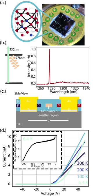
In this article, we investigate the cryogenic optical response of a silicon color center to an applied electric field by integrating an ensemble of G centers with lateral p+-p-n+ diodes fabricated in silicon on insulator (SOI) (Fig. 1a). The G center–comprised of two substitutional carbon atoms bonded to an interstitial silicon atom–is an optically-active O-band emitter (Fig. 1b). Hydrogen implantation was found to be necessary for formation of G centers within our devices, and an ensemble is thereby localized to the middle of the diode junction by implanting hydrogen ions with a lithography-defined mask (Fig. 1c) in a wafer previously blanket-implanted with carbon. Above a spatially-dependent threshold voltage, the ensemble zero phonon line (ZPL) experiences a redshift up to 100 GHz at a rate of approximately 1.4 GHz/V. Additionally, we observed the continuous reduction of the G center optical fluorescence with increasing reversed bias voltage, and at -210V the fluorescence was fully suppressed. Finally, we employ the observed emitter-field coupling to image the spatial distribution of the electric field within the junction.
The resultant spatial dependence of ZPL tuning and ensemble extinction suggest these mechanisms could be attributed to a combination of the Stark effect and Fermi-level shifting via band-bending. Our method has broad applicability for future control in quantum networking experiments, and serves as a tool for probing fundamental color center behavior. This approach is readily extensible to probe and control other color centers in silicon, and color centers in a wide range of semiconductor platforms which are easily doped, such as silicon carbide.
II Lateral diodes with integrated G center ensemble
We sought to realize a spatially-isolated G center ensemble maximally interacting with an electrical diode at a buried plane which is ultimately compatible with integrated silicon photonics. The maximum optical mode concentration of photonic crystal cavities in a 220 nm silicon layer would reside at 110 nm, thus we implement a design and fabrication strategy to support future hybrid electrical-optical coupling of semiconductor quantum emitters. To facilitate this, an industry standard 220 nm SOI wafer was utilized, with a dopant-defined diode embedded at a depth of 110 nm. Ion implantation combined with successive aligned optical lithography writes enabled masked localized incorporation of the p- and n- dopants, and the G center ensemble, at the desired depth. An etch-defined metallization strategy was employed to ensure robust electrical contact and performance at the dopant plane, and the device was packaged for cryogenic characterization. The current-voltage characteristics of the devices (Fig. 1d) do not degrade with temperature or masked hydrogen implantation, and they exhibit low leakage current under high reverse bias (Fig. 1d inset).
II.1 Device Design and Fabrication
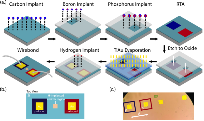
Lateral diodes are fabricated in commercial SOI (University Wafer, 220 nm Si on 2 m buried oxide insulator, boron-doped, cm, orientation) to facilitate simultaneous cryogenic optical and electrical measurement of color centers. The starting substrate of the devices is lightly p-doped based on prior reports of emitter synthesis [17, 14], though electrical performance would be improved in intrinsic material. The device design enables ease of optical access, variable junction width, and wafer scale–where hundreds of devices with swept parameters can be fabricated on a single commercial wafer defined via optical lithography. Further, the design co-locates the formed color centers and dopant-defined junction in the same spatial plane, improving emitter-field interaction. Device performance is validated with the COMSOL Multiphysics Semiconductor Module (see SI). The full device design and fabrication is depicted in Fig. 2a. An top-down diagram of the relevant regions of the device is illustrated in Fig. 2b, accompanied by an optical image of the finished devices (Fig. 2c). The full details of device fabrication are given in Methods.
II.2 Ensemble Incorporation
To form G centers within the diodes, we first implant Si with carbon ions then rapid thermal anneal at 1000°C to heal lattice damage. However, in contrast to some previous work [17, 15, 25, 16], we did not observe G centers at this stage. Consistent with the findings of other works arguing proton irradiation facilitates incorporation of interstitial carbon into G centers [26, 11], we investigated varied means of hydrogenation to complete the G center formation (see SI [27]). Masked ion implantation of hydrogen was ultimately selected for the device-emitter integration to obtain a bright localized ensemble at the targeted depth where the electric field is strongest, with negligible degradation of electrical performance. Consistent with the findings of hydrogen’s role in G center formation and stabilization, we found ensemble emission localized only to the implantation mask. Additionally, we found the G center to be unstable above 200°C [27], consistent with previous work [28], therefore requiring hydrogen incorporation to be the final fabrication step. Thus to ensure the diode fabrication was compatible with G center production, steps for both fabrication processes were interspersed.
III Electrical manipulation
Applying reverse-bias to a diode yields several electrical signatures: Fermi level engineering via band bending, generation of a depletion region with a local electric field internal to the junction, and suppression of leakage current. For junction-integrated color centers, band bending and junction depletion modulate the observed photoluminescence spectra, while low leakage current ensures minimal local heating. We first characterized the optical response of both the silicon free-exciton and the diode-integrated G center ensemble localized to the hydrogen implantation aperture under application of a reverse-bias DC electric field. Then the distribution of ensemble optical response is investigated across the junction, where competing effects from band bending and junction depletion can be distinguished.
III.1 Reverse bias
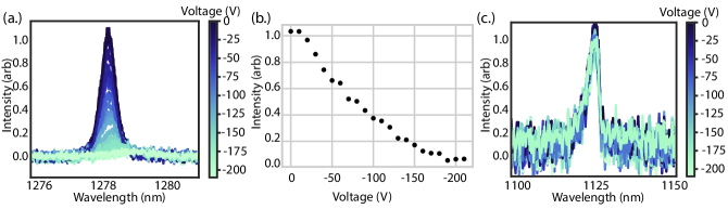
The G center ensemble response to a reverse-biased DC electric field is shown in Fig. 3a-b. Photoluminescence was measured while sweeping the reverse bias in 10 V intervals from 0 to -210 V (Fig. 3a). The fluorescence intensity of the ensemble reduced as a function of increasing reverse bias until the signal dropped below the noise floor of the measurement (Fig. 3b). A 100 GHz redshift at a rate of approximately 1.4 GHz/V was observed in the G center ZPL above a spatially-dependent threshold voltage (explored in detail in Section III B). Additionally, the ensemble linewidth broadened as the center wavelength redshifted (see SI [27]). Both the ensemble redshift and linewidth broadening rates exhibit discontinuities from an ideal linear trend–this could be explained by the distribution of Stark shifts for each emitter within the confocal spot due to the varied dipole alignments within the ensemble. Future experiments with single emitters may elucidate whether the observed linewidth broadening and shifting is dominated by the local electric field interaction or via band-bending.
Reverse biased current of -0.5 µA was passed at -200 V–corresponding to an applied power of 100 µW spread over a 103 µm junction gap. The device maintained low leakage current at high reverse bias, thus local heating is unlikely to be the source of the observed G center broadening, shifting, and modulation. To illustrate this point, the evolution of the silicon free-exciton line was investigated under the same bias conditions (Fig. 3c). The silicon free-exciton is suppressed at elevated temperature (Supplementary Information [27]) and thus served as a probe of local junction heating. The exciton photoluminescence (PL) measured from 0 to -210 V is shown in Fig. 3c. The exciton luminescence was not modified under reverse bias, consistent with the absence of significant heating–with fluctuations attributable to noise in the experiment. These results of the G center and silicon free-exciton are contrasted with the behavior under application of a high power forward bias in the supplementary information [27].
III.2 Spatial Distribution of Emitter-Field Coupling
Capturing the distribution of emitter optical response across the junction can aide in characterizing the nature of the emitter-field interaction. Band bending is achieved simply by making the p-contact increasingly negative and should be evident across the junction to varying degree. The Fermi level is a critical factor in a color center’s optical activity [29, 30, 31], and thus an ensemble brightness gradient is expected to be present across the junction in proportion to the band bending achieved at a given voltage if the energy required for ionization is commensurate with the supplied electric potential [32, 33]. Conversely, excess carriers in the junction prevent complete depletion below a critical threshold voltage [7, 34]. The starting substrate of these devices is lightly p-doped and thus the depletion region is expected to be nonuniform, reaching the ensemble at a sufficiently large threshold voltage emerging first near the n-contact. Stark effect is mediated by a local electric field experienced by the ensemble, and thus is observed only when the depletion region reaches the ensemble [7, 34].
Additionally, the depletion region of the junction can be monitored directly by measuring confocal photocurrent, and hence one can correlate the depletion region’s spatial occurrence confirmed via photocurrent with an optical response of the ensemble. To this end, the spatial distribution of the electric-field coupling to the G center ensemble is imaged (Fig. 4 top row), and correlated with the associated optically-generated photocurrent (Fig. 4 bottom row) of the diode under 0-bias (Fig. 4a), -100 V (Fig. 4b), and -200 V (Fig. 4c.).
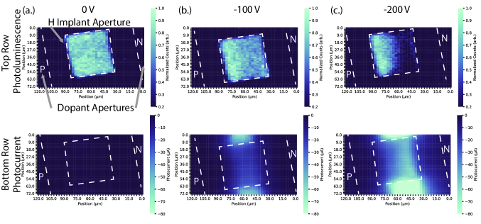
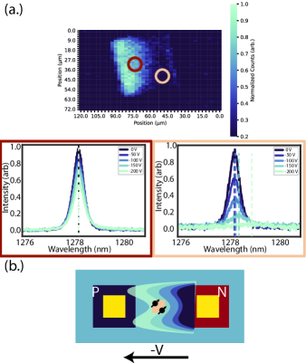
At 0 V, the localization of the G center ensemble is clear (Fig. 4a top). G center PL is only observed in the 5050m aperture at the center of the diode through which hydrogen was implanted. As expected under zero bias, the measured photocurrent is negligible (Fig. 4a bottom).
The confocal scan was repeated across the junction at a reverse bias of -100 V (Fig. 4b). At -100 V, the optical intensity modulation ratio of the G centers was spatially dependant, with the emitters in the portion of the hydrogen-implant aperture closest to the n-contact showing 40% greater suppression in response to the applied electric field than those nearest the p-contact. Interestingly, when comparing the confocal PL (top) with the associated confocal photocurrent measured in the device (bottom), the presence of the ensemble–and thus hydrogen–decreased the current passage across the junction, as the regions within the junction above and below the implant aperture demonstrated higher photo-responsivity.
Finally, the confocal PL and photocurrent spatial scan was repeated at a reverse bias of -200 V (Fig. 4c). Closer to the n-type contact, 100% modulation of the G center fluorescence is observed (Fig. 4c top). Conversely, closer to the p-contact, G centers are minimally suppressed. Furthermore, the associated confocal photocurrent (Fig. 4c bottom) follows the same spatial pattern. Optically-generated photocurrent measured in the junction was maximum in the region where emission is maximally modulated, confirming that the region of greatest depletion corresponds with strongest emitter interaction. As the strength of the reverse bias field increased, the spatial extent of the ensembles experiencing greatest optical modulation spread from the n-contact toward the p-contact as electrons and holes are swept toward their respective n- and p- contacts (Fig. 4 a-c).
Furthermore, although partial optical modulation was observed at the center of the junction, wavelength tuning was not (Fig. 5a red). This finding is consistent with those reported experimentally in [7], and theoretically in [34], where at reverse bias voltages below a critical value, the size of the depletion region is less than the width of the junction. In [7], the threshold voltage to observe Stark effect of single divacancies in 4H-silicon carbide positioned at different spatial planes of a vertical diode depended on the position of the emitter in the junction. Here, we extend this argument by directly imaging the spatial dependence of the entire diode depletion region. Above a spatially-dependent threshold voltage where the junction depletion reaches the ensemble, a continual redshift of approximately 1.4 GHz/V is observed (Fig. 5a brown) [27]. However tens of microns away, where the junction depletion has not yet reached the ensemble, no wavelength tuning is experienced (Fig. 5a red). From these findings, precise determination of the G center differential polarizability is obfuscated due to the non-uniform field distribution in the junction and the distribution of dipole orientations within the ensemble [16]. However future work using single emitters in an undoped I layer of a PIN diode would enable this estimation to compare with theoretical predictions of the permanent dipole moment [35], as the precise Stark shift rate would be clearly captured by a single emitter and the lack of residual dopants would result in improved electric field uniformity. Wavelength-tuning is only observed in regions that also exhibit strong photocurrent, indicating the presence of the junction depletion region and large local electric field. This observation is conceptually illustrated in (Fig. 5b). These results suggest the Stark effect could be responsible for the observed emitter red-shift. The boron dopants in these areas within the junction are sufficiently depleted such that electric field can build up to yield Stark-shifted G centers.
Finally, G center optical intensity is modulated both within and outside of the depletion region under increasing reverse bias. This observation could be explained by considering the effects of band-bending. The G center is thought to possess a bi-stability in its atomic configuration between an optically-active B configuration and a dark A configuration [32]. Optical emission arises in the transition from the meta-stable A to the B form under photo-injection [32, 11, 33]. G center ensemble brightness thus depends upon the concentration of B configuration emitters: for lightly p-doped silicon at 4 K, the concentration of A configuration emitters should dominate B configuration emitters. However, optical excitation enables conversion of A configuration emitters to the metastable B configuration, where they can photoluminesce. Further, both A and B configuration emitters can be ionized to non-emissive charge states as the fermi level is tuned under external bias [32, 33]. Our observations are consistent with this explanation: as we increase the reverse bias across the junction, emitters in the A configuration convert to the emissive B configuration, but are probabilistically ionized to a dark state as a function of the resultant band bending.
IV Conclusion
We probed the coupling of a telecommunication-band silicon color center to DC electric fields by integrating G centers into diodes while retaining optical access. We then utilized the electrical manipulation of the ensemble to image the electric-field distribution within the diode, capturing the spatial evolution of the junction depletion region across varied reverse-bias voltages. Within the junction depletion region the ZPL redshifted by approximately 100 GHz at a rate of 1.4 GHz/V above a threshold voltage, whereas only modulation of the ZPL fluorescence intensity is observed outside of the depletion region. These findings suggest distinct emitter-field couplings are exhibited–with a spatial dependence across the junction–where band-bending and Stark effect could explain the observed phenomena. Furthermore, we find that hydrogen plays a critical role in the ability to observe G centers in our devices. To this end, future work will continue to elucidate the specific mechanisms involved in G center formation and stabilization, both via hydrogenation and electrical control.
These devices provide a tool for electrically manipulating color centers with broad applicability to both other silicon color centers, and color centers in other semiconductor platforms. These findings using an ensemble of color centers to illustrate the spatial distribution of emitter-field coupling in the junction will motivate and inform the design of electrical devices to optimally couple to a single emitter. It would be of particular interest to observe the response of silicon T centers to electrical tuning via diode, as T centers possess a coherent spin-photon interface [14], and are reported to follow a similar synthesis procedure as was implemented here. Furthermore, our demonstration of the direct visualization of electric field dynamics in a semiconductor–optically mapping a DC electric field in-situ–has application in quantum sensing of electric fields [36]. Finally, our lateral diode design at a buried plane of 110 nm is compatible with photonic crystal cavity integration [37, 38], where future work intends to enable simultaneous electrical tuning, stabilization, and control of cavity-enhanced quantum emitters.
V Methods
V.1 Fabrication
All carbon, hydrogen, boron, and phosphorus ion implantation was performed at INNOViON Corporation. Ion implantation energies are determined using Stopping Range of Ions in Matter (SRIM) calculations [27], targeting a depth of approximately for each ion. Dopant densities are selected to obtain an acceptor/donor concentration of 1/cm3 at the desired depth, as this order magnitude is typical of electrical devices in silicon. Further, overlapping the maximum dopant concentration depth with the etch-defined metalization ensures transmissive metal-semiconductor interface for ohmic contact. Each implantation was performed at a tilt. All masked implantation utilized optical lithography in the positive photoresist mask S1813 at a fluence of 250 mJ and wavelength of 375 nm using a Heidelburg Maskless Aligner 150. The resist was pre-baked at for 3 minutes, and developed for 70 seconds in TMAH-based CD-26. Every photoresist mask was stripped with a 500 W plasma, and the Ti-Au resist-on-liftoff mask was stripped with a 12 hr soak in remover PG at .
First, an unmasked bulk wafer fragment is implanted with 7/cm2 12C ions at an energy of 38 keV. Next, m apertures are written in a photoresist mask with optical lithography, and 1/cm2 11B ions are implanted at an energy of 29 keV through the apertures to define localized p-doped islands. After resist stripping, n-doped islands are generated by implanting 1/cm2 31P ions at an energy of 80 keV through offset 500500m apertures again defined with optical lithography. The spacing between the p- and n-doped apertures (Fig. 2b) is swept across the wafer to vary the strength of the junction electric field for a given voltage. To both heal the crystal lattice and incorporate the dopants substitutionally in the silicon lattice [28], a rapid thermal anneal (RTA) is performed at C for 20 seconds in an argon environment after stripping the resist.
Next, electrical contacts are generated by first writing 250250m apertures in a new resist mask positioned such that each opening was aligned to the center of the implanted dopant islands. Using SF6 and C4F8 chemistry in a reactive ion etching chamber, the exposed windows are then etched down 220 nm to the oxide to ensure optimal overlap of the metal contacts with the implanted dopants. Following definition of a new 300300m aperture mask of photoresist on lift-off (S1813 on LOR3A), also aligned to the center of the implanted dopant islands, a thin film of 300 nm gold on a 30 nm titanium adhesion layer (Ti-Au) is deposited via electron beam evaporation.
To complete the incorporation of G center ensembles, hydrogen is implanted through a window at the center of each junction (Fig. 2b). 7/cm2 H ions were implanted at an energy of 9 keV through 5050m apertures in a final resist mask, forming an ensemble of diode-integrated G centers. The wafer fragment was subsequently diced into 66 mm samples that were integrated into a 16-pin electrically-wired cryogenic cold-finger and wire-bonded for external driving (Fig. 1a).
V.2 Experimental Setup
Experiments are performed in a home-built confocal microscope using a Mitutoyo 100 0.5 NA Near-IR objective. G centers are optically excited using an off-resonant diode-pumped solid-state laser, and junctions are biased using a Keithley 2400 source meter. Simultaneous optical and electrical measurements are enabled in a Janis ST-500 continuous-flow Helium-cooled cryostat with a 16-pin mapped electrical feed-through wire-bonded to the diodes. The system achieves a base temperature of roughly 6 K. Photoluminescence of the diode-integrated color centers is measured on an Acton Spectra Pro 2750 spectrograph with a Princeton Instruments OMA:V indium-gallium-arsenide nitrogen-cooled photodiode array detector. Raman spectroscopy is performed in a LabRAM Evolution Horiba multi-line room-temperature confocal Raman spectrometer using 532 nm laser excitation.
VI Author contributions
Methodology: A.M.D., M.S., J.R.D., D.D.S., M.K.B., E.L.H; Fabrication: A.M.D., A.R.; Measurement: A.M.D., J.R.D.; Analysis: A.M.D., M.S., J.R.D., D.D.S., M.K.B., E.L.H; Advising: D.D.S., M.K.B., E.L.H; Manuscript Preparation: All authors.
VII Acknowledgments
This work was supported by AWS Center for Quantum Networking and the Harvard Quantum Initiative. Portions of this work were performed at the Harvard University Center for Nanoscale Systems (CNS); a member of the National Nanotechnology Coordinated Infrastructure Network (NNCI), which is supported by the National Science Foundation under NSF award no. ECCS-2025158. M.S. acknowledges funding from a NASA Space Technology Graduate Research Fellowship.
VIII Data Availability
The data that support the findings of the work are available from the corresponding author upon reasonable request.
References
- Bhaskar et al. [2020] M. K. Bhaskar et al., Experimental demonstration of memory-enhanced quantum communication, Nature 580, 60 (2020).
- Knall et al. [2022] E. Knall et al., Efficient source of shaped single photons based on an integrated diamond nanophotonic system, Physical Review Letters 129, 053603 (2022).
- Stas et al. [2022] P.-J. Stas et al., Robust multi-qubit quantum network node with integrated error detection, Science 378, 557 (2022).
- Pompili et al. [2021] M. Pompili et al., Realization of a multinode quantum network of remote solid-state qubits, Science 372, 259 (2021).
- Rosenthal et al. [2023] E. I. Rosenthal et al., Microwave spin control of a tin-vacancy qubit in diamond, Phys. Rev. X 13, 031022 (2023).
- Miao et al. [2020] K. C. Miao, J. P. Blanton, C. P. Anderson, A. Bourassa, A. L. Crook, G. Wolfowicz, H. Abe, T. Ohshima, and D. D. Awschalom, Universal coherence protection in a solid-state spin qubit, Science 369, 1493 (2020).
- Anderson et al. [2019] C. P. Anderson et al., Electrical and optical control of single spins integrated in scalable semiconductor devices, Science 366, 1225 (2019).
- Lukin et al. [2020a] D. M. Lukin et al., 4h-silicon-carbide-on-insulator for integrated quantum and nonlinear photonics, Nature Photonics 14, 330 (2020a).
- Babin et al. [2022] C. Babin et al., Fabrication and nanophotonic waveguide integration of silicon carbide colour centres with preserved spin-optical coherence, Nature materials 21, 67 (2022).
- Day et al. [2023] A. M. Day, J. R. Dietz, M. Sutula, M. Yeh, and E. L. Hu, Laser writing of spin defects in nanophotonic cavities, Nature Materials 22, 696 (2023).
- Beaufils et al. [2018] C. Beaufils et al., Optical properties of an ensemble of g-centers in silicon, Physical Review B 97, 035303 (2018).
- Bergeron et al. [2020] L. Bergeron, C. Chartrand, K. Kurkjian, A.T.K. andMorse, H. Riemann, N. Abrosimov, P. Becker, H. Pohl, M. Thewalt, and S. Simmons, Silicon-integrated telecommunications photon-spin interface, PRX Quantum 1, 020301 (2020).
- Durand et al. [2021] A. Durand et al., Broad diversity of near-infrared single-photon emitters in silicon, Physical review letters 126, 083602 (2021).
- Higginbottom et al. [2022] D. B. Higginbottom et al., Optical observation of single spins in silicon, Nature 607, 266 (2022).
- Komza et al. [2022] L. Komza et al., Indistinguishable photons from an artificial atom in silicon photonics, arXiv preprint arXiv:2211.09305 (2022).
- Redjem et al. [2023] W. Redjem et al., All-silicon quantum light source by embedding an atomic emissive center in a nanophotonic cavity, Nature Communications 14, 3321 (2023).
- Prabhu et al. [2023] M. Prabhu, C. Errando-Herranz, L. De Santis, I. Christen, C. Chen, C. Gerlach, and D. Englund, Individually addressable and spectrally programmable artificial atoms in silicon photonics, Nature Communications 14, 2380 (2023).
- DeAbreu et al. [2023] A. DeAbreu et al., Waveguide-integrated silicon T centres, Optics Express 31, 15045 (2023).
- Lee et al. [2023] C.-M. Lee, F. Islam, S. Harper, M. A. Buyukkaya, D. Higginbottom, S. Simmons, and E. Waks, High-efficiency single photon emission from a silicon T-center in a nanobeam, arXiv preprint arXiv:2308.04541 (2023).
- Rühl et al. [2019] M. Rühl, L. Bergmann, M. Krieger, and H. B. Weber, Stark tuning of the silicon vacancy in silicon carbide, Nano Letters 20, 658 (2019).
- Lukin et al. [2020b] D. M. Lukin et al., Spectrally reconfigurable quantum emitters enabled by optimized fast modulation, npj Quantum Information 6, 80 (2020b).
- de las Casas et al. [2017] C. F. de las Casas, D. J. Christle, J. Ul Hassan, T. Ohshima, N. T. Son, and D. D. Awschalom, Stark tuning and electrical charge state control of single divacancies in silicon carbide, Applied Physics Letters 111 (2017).
- Widmann et al. [2019] M. Widmann et al., Electrical charge state manipulation of single silicon vacancies in a silicon carbide quantum optoelectronic device, Nano letters 19, 7173 (2019).
- Niethammer et al. [2019] M. Niethammer et al., Coherent electrical readout of defect spins in silicon carbide by photo-ionization at ambient conditions, Nature communications 10, 5569 (2019).
- Hollenbach et al. [2022] M. Hollenbach et al., Wafer-scale nanofabrication of telecom single-photon emitters in silicon, Nature Communications 13, 7683 (2022).
- Baron et al. [2022] Y. Baron et al., Single g centers in silicon fabricated by co-implantation with carbon and proton, Applied Physics Letters 121 (2022).
- [27] Supplementary information.
- Canham et al. [1987] L. Canham, K. Barraclough, and D. Robbins, 1.3-m light-emitting diode from silicon electron irradiated at its damage threshold, Applied physics letters 51, 1509 (1987).
- Son and Ivanov [2021] N. T. Son and I. G. Ivanov, Charge state control of the silicon vacancy and divacancy in silicon carbide, Journal of Applied Physics 129 (2021).
- Zhang et al. [2023] Z. Zhang, J. Zuber, L. Rodgers, X. Gui, P. Stevenson, M. Li, M. Batzer, M. GrimauPuigibert, B. Shields, A. Edmonds, N. Palmer, M. Markham, R. Cava, P. Maletinsky, and N. de Leon, Neutral silicon vacancy centers in undoped diamond via surface control, Physical review letters 130, 166902 (2023).
- Pederson et al. [2023] C. Pederson, R. Giridharagopal, F. Zhao, S. T. Dunham, Y. Raitses, D. S. Ginger, and K.-M. C. Fu, Optical tuning of the diamond fermi level measured by correlated scanning probe microscopy and quantum defect spectroscopy, arXiv preprint arXiv:2309.15969 (2023).
- Song et al. [1990] L. Song, X. Zhan, B. Benson, and G. Watkins, Bistable interstitial-carbon–substitutional-carbon pair in silicon, Physical Review B 42, 5765 (1990).
- Udvarhelyi et al. [2021] P. Udvarhelyi, B. Somogyi, G. Thiering, and A. Gali, Identification of a telecom wavelength single photon emitter in silicon, Physical review letters 127, 196402 (2021).
- Candido and Flatté [2021] D. R. Candido and M. E. Flatté, Suppression of the optical linewidth and spin decoherence of a quantum spin center in a p-n diode, PRX quantum 2, 040310 (2021).
- Ivanov et al. [2022] V. Ivanov et al., Effect of localization on photoluminescence and zero-field splitting of silicon color centers, Physical Review B 106, 134107 (2022).
- Dolde et al. [2011] F. Dolde et al., Electric-field sensing using single diamond spins, Nature Physics 7, 459 (2011).
- Bracher et al. [2017] D. O. Bracher, X. Zhang, and E. L. Hu, Selective purcell enhancement of two closely linked zero-phonon transitions of a silicon carbide color center, Proceedings of the National Academy of Sciences 114, 4060 (2017).
- Crook et al. [2020] A. L. Crook et al., Purcell enhancement of a single silicon carbide color center with coherent spin control, Nano letters 20, 3427 (2020).