Ultra-large polymer-free suspended graphene films
Abstract
Due to its extraordinary properties, suspended graphene is a critical element in a wide range of applications. Preparation methods that preserve the unique properties of graphene are therefore in high demand. To date, all protocols for the production of large graphene films have relied on the application of a polymer film to stabilize graphene during the transfer process. However, this inevitably introduces contaminations that have proven to be extremely difficult, if not impossible, to remove entirely. Here we report the polymer-free fabrication of suspended films consisting of three graphene layers spanning circular holes of 150 diameter. We find a high fabrication yield, very uniform properties of the freestanding graphene across all holes as well across individual holes. A detailed analysis by confocal Raman and THz spectroscopy reveals that the triple-layer samples exhibit structural and electronic properties similar to those of monolayer graphene. We demonstrate their usability as ion-electron converters in time-of-flight mass spectrometry and related applications. They are two orders of magnitude thinner than previous carbon foils typically used in these types of experiments, while still being robust and exhibiting a sufficiently high electron yield. These results are an important step towards replacing free-standing ultra-thin carbon films or graphene from polymer-based transfers with much better defined and clean graphene.
I Introduction
Ultrathin carbon films are key materials for many applications and experiments. Supported films are used for example as coating for battery electrodes [1] or as sensors for virus detection [2]. A very important and large field of applications stems from the fact that ion irradiation of solids leads to the emission of electrons [3, 4]. Thus, supported carbon films are, e.g., used in space instrumentation for incident ion detection [5, 6, 7, 8], while suspended carbon foils are frequently used in coincidence- and time-of-flight (ToF) measurements [9, 10, 11], or for stripping purposes, i.e. the ionization of energetic neutral atoms and charge equilibration of ions [12, 13].
With the discovery of graphene (Gr), it became for the first time possible to prepare suspended carbon films of high structural quality [14] that are two orders of magnitude thinner than the thinnest conventional carbon foils. This has led to even more advanced applications such as ultrasensitive pressure sensors and actuators [15, 16, 17, 18, 19] windows for in vivo/in situ scanning electron microscopy [20] as well as X-ray photoelectron spectroscopy [21], and membranes for ultrafiltration [22, 23, 24, 25].
Suspended graphene is in particular well-suited for studying and exploiting ion-solid interactions, as it exhibits a high structural quality and a well-defined thinness. Further, it has not only been shown to be mechanically robust [26, 27, 28] and extremely radiation hard [29, 30, 31, 32, 33] but it also features an outstanding self-healing capability [34] making it superior to any other material. Thus it comes as no surprise, that exfoliated graphene, suspended on transmission electron microscopy (TEM) grids has helped to significantly advance our understanding of ion-solid-interactions [32, 35].
However, the samples used in these studies have been extremely small and the fabrication of suspended graphene targets, that are sufficiently large (i.e. much larger than the areas typical for a TEM grid) and clean, poses a serious challenge. In particular, polymers, which are frequently used in the preparation of large suspended graphene samples (see e.g. ref. [15]), cannot be completely removed, and even worse, often form a homogeneous film, as recently shown by Tilmann et al. [36]. This can however not be tolerated in most cases, as e.g. these unavoidable residues would prevent the interaction of ions with graphene. Furthermore, for any time-sensitive experiment, the samples also need to be extremely flat in order not to negatively affect the time-resolution as will be discussed in more detail below.
In this paper we report how such suspended large-area, high quality graphene targets can be fabricated from commercially available graphene grown by chemical vapour deposition (CVD) without the use of polymers. We present a detailed study of their structural and electronic properties revealed by optical profilometry as well as confocal Raman- and THz spectroscopy. Finally, we show that these targets despite their thinness can be used as efficient ion-to-electron converters and are thus indeed suitable targets for fundamental research and as well for applications in the field of ion-solid-interaction.
II Preparation of large area, contamination free graphene
To avoid the contamination of our samples we have established a completely polymer-free wet transfer process. The preparation process starts by applying a procedure that we have developed earlier to increase the mechanical stability of graphene and funtionalize it (for details see [37]). Briefly, a Gr/Cu wafer produced by CVD is placed into an ethylene-vinyl acetate co-polymer foil together with a supporting solid, smooth plate. The Gr/Cu wafer package is then put into a plastic bag that is evacuated and sealed with a commercially available vacuum sealer. The Gr/Cu wafer stays in contact with the co-polymer foil under these vacuum conditions for at least 24 hrs. After the seal is broken, the wafer is cut into pieces of roughly 10 mm x 10 mm and placed into an ammonium persulfate solution of 20 % concentration. After the copper is fully dissolved, the etching solution is diluted by de-ionized (DI) water and the graphene floating on the surface is scooped onto another Gr/Cu piece.
After the stack is fully dry, this process is repeated until the desired number of graphene layers is obtained. For reasons which will become apparent in below, we will refer to these as double (and not bilayer), triple or quadruple layers. In the final step, the stack is etched in the manner previously described, then transferred onto a substrate of 250 thick silicon (Si), or steel plate, featuring a periodic matrix of 200 holes, with a diameter of 150 each, created by laser ablation.
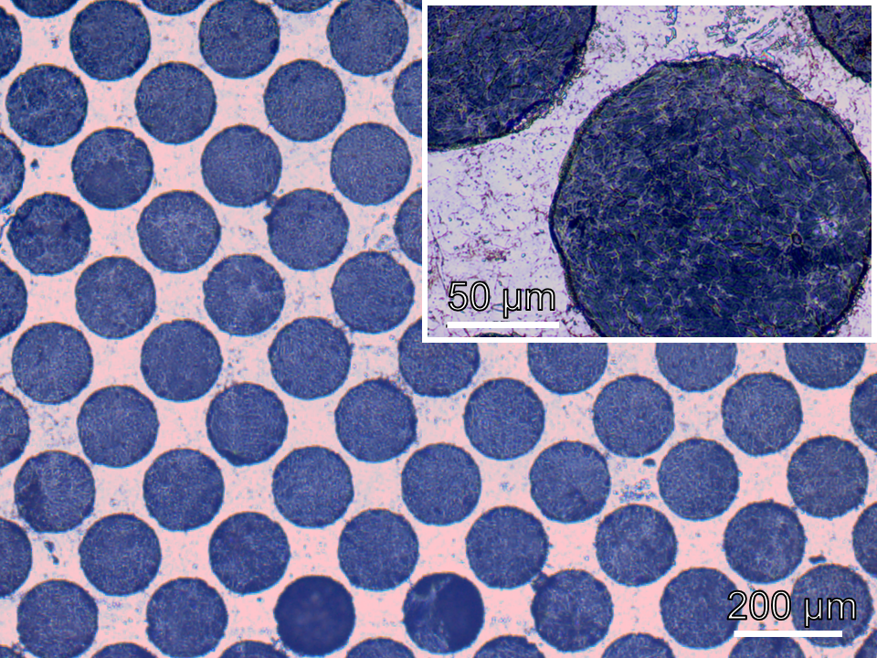
In principle, targets with double layers of graphene can be manufactured in this way, but then the coverage of holes is insufficient. This might be due to the fact that CVD graphene is known to have a reduced mechanical stability compared to exfoliated graphene because of more grain boundaries [38]. These grain boundaries are susceptible to tearing if not reinforced by an additional layer. In the case of double layer graphene, the likelihood of two mechanically weak points aligning may still be significant enough to result in a reduced coverage.
In contrast, triple layer graphene stacks exhibit sufficient stability, as evidenced by the freestanding graphene layers spanning 150 shown in Fig 1. The overall coverage is typically 90 % for triple layers, and with additional layers, an even higher coverage can be achieved. In the following, we will focus on triple layers of graphene, as this represents a good compromise between minimum thickness and a sufficiently high coverage.
III Properties
III.1 Optical Profilometry: Topography
To obtain a non-destructive representation of the topography, we utilized a 3D optical profilometer (S Neox 090 Sensofar). A typical false color image can be seen in Fig. 2 a. In this example, graphene covers the complete hole of 150 and is almost plane-parallel to the Si-substrate surface as can be seen from the line scan in the inset of Fig. 2 a. With the help of such line scans we could identify two more topography types within the holes as depicted by the blue dotted lines in Fig. 2 b.
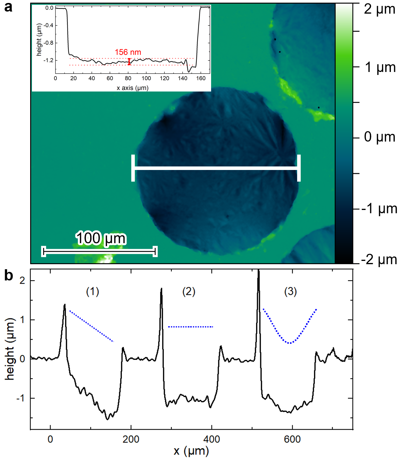
These three types of topography result in distinctive height differences. Type (1) shows a slope with the largest height difference, while type (2) is plane parallel and results in the smallest possible one. Type (3), the hammock-like, results in an intermediate height difference. This is an important quantity for samples used as a target material in any time-sensitive experiment because one needs to know the exact starting point of the emitted particles in order to evaluate their flight time with respect to a given time zero.
To illustrate this more clearly, let us look at an example. Ultra thin carbon foils are frequently used to generate a START-signal for coincidence- or ToF measurements because ions cause electron emission when passing through such foils [39]. If we would use a graphene target like the one seen in Fig. 2 a, with the maximal height deviation of 156 nm, an ion impact would thus in the worst case take place either at the highest point of the graphene target or at the lowest, respectively. For a pulse of Ne+ ions with 3.5 keV energy, e.g., this would result in a time difference for the arrival of the ions and thus the emission of any secondary particles corresponding to:
This is well below the time-resolution of any current experiment and thus, graphene targets of type (2) are the best case scenario, as all emitted particles would practically start at the same time after the ion impact. Graphene targets of type (1) exhibit a maximum height difference of over 1 which seems large in light of the discussion above. However, it is rather easy to correct for this difference by tilting the graphene surface to become plane-parallel. After plane-subtraction the remaining mean height variation for this type is typically on the order of (100–300) nm, similar to type (2). In contrast, type (3) targets resemble a ”hammock”, for which there is no way of correction possible and therefore are not suitable for time critical experiments. However, with only 4 % occurrence this type is relatively rarely seen in our samples with a fully covered target, while 42 % are of type (2) and 54 % of type (1), respectively.
III.2 Raman: Structure, Strain and Doping
High quality films should not just be flat but should also feature similar properties over the whole sample area. We therefore probed the homogeneity of graphene within the holes using Raman spectroscopy. The positions of the two characteristic modes of graphene, namely the and mode allow for a determination of layer number, charge carrier density, and mechanical strain as shown by Lee et al [40] and Kim et al. [41].
Single-point spectra (not shown here) of our triple layer samples resemble spectra of monolayer graphene and thus do not show the typical signature of a bilayer graphene. In order to get better statistics and to compare different holes, we utilized the extended area mapping feature of a Renishaw InViaTM confocal Raman microscope. In Fig. 3 a and b, such maps featuring 14 holes are presented, showcasing both the position of the mode and that of the mode. In case of the mode, the holes can be clearly distinguished from the surrounding Si substrate, while in the case of the mode, the holes appear more blurry.
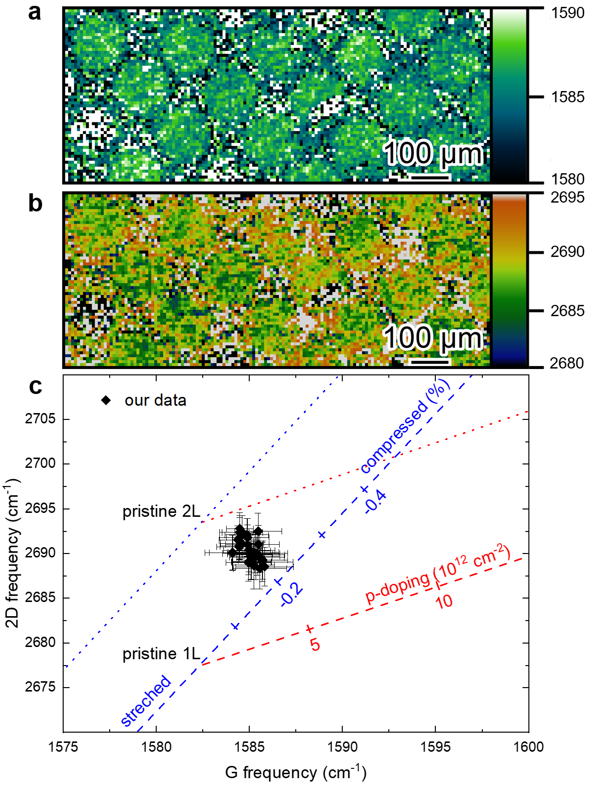
From each hole, 276 data points were collected, with a step size of 8 per data point, and are summarized via the software package Gwyddion [42] yielding a probability distribution of the mode positions which is then fitted with a Gaussian function. Thus, each data point in Fig. 3 c corresponds to an individual hole, with the error bars indicating the standard deviation for the corresponding average value of this particular hole. To this plot, we have added the linear functions (dashed lines) established by Lee et al. [40] representing the shift of the Raman modes of monolayer graphene in the presence of strain (blue) and charge carriers doping (red). The position of the Raman modes for pristine monolayer graphene is given by the intersection. For bilayer graphene, the respective data is shifted [41] and presented here by the dotted lines.
As Fig. 3 c shows, we find constant strain and doping levels within each hole and a remarkable reproducibility across the different holes. Notably, our data from triple layer graphene lies in between the values for mono- and bilayer graphene indicating a decoupling of the respective layers, as also shown in the single-point spectra indicating a monolayer of graphene. This makes a straightforward quantification of our data difficult. If we take bilayer graphene as a reference [41] for quantification, averaging over all our data points and using the vector model of Lee et al., we would arrive at hole doping with (5.51.5)1012 cm-2 and tensile strain of (0.20.09) %. While these numbers might give a first indication that the triple layers are slightly strained and -doped, we chose a complementary approach to gain further insight into the electronic properties of our graphene samples.
III.3 THz spectroscopy: Mobility and charge carrier density
Terahertz (THz) spectroscopy is a versatile tool to investigate the carrier density and mobility without the need of electrical contacts [43], the processing of which would again contaminate our samples. In particular, in thin conductive films like graphene, the interaction with THz radiation is dominated by intraband absorption [44]. Due to the large wavelength of 300 at 1 THz photon frequency, the spot size of conventional THz spectrometers is on the order of about 1 mm and thus requires large samples. To overcome this obstacle, we performed the THz measurements with an all optical near-field microscope [45] by bringing our graphene samples in close proximity to an electro-optical crystal (ZnTe, compare Fig. 4 a. Note, that for these experiments we had to use the steel substrates with holes in it, due to the fact that the quality of the Si hole edges was not sufficient enough. A near-infrared beam serves as probe to measure the THz transient.
The spatial resolution is in this case mostly dependent on the numerical aperture of the near-infrared beam and the thickness of the electro-optical crystal. With a 150 µm thick ZnTe crystal, we can resolve objects smaller than 100 . A sketch of the near-field optics is shown in Fig. 4 a. To analyze the data with a thin film model, the refractive index of the substrate needs to be known. This was measured by comparing the transmission through one of the uncovered holes with the impinging THz field, the result is plotted in Fig. 4 b.
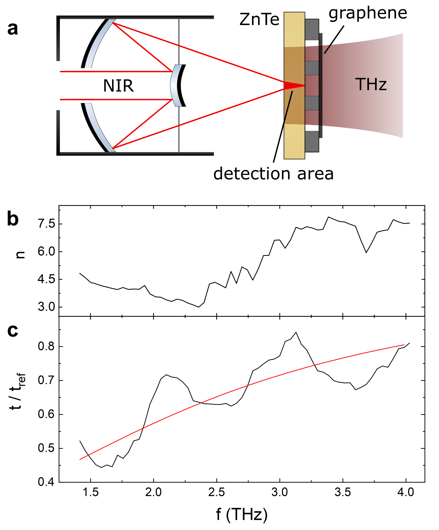
The freestanding graphene triple layer was then measured by comparing the transmission through a hole covered by graphene with a reference measurement through a bare hole. As the optical properties of the ZnTe crystal can vary spatially due to defects, we performed reference measurements for each of the sample measurements through neighboring holes, the resulting transmission spectra were averaged to reduce noise. The spectrum of the transmitted electric field is shown in Fig. 4 c. The oscillations that can be observed in the spectrum are caused by multiple reflections in the ZnTe crystal and cannot be entirely avoided due to the dispersion in the metallic hole.
A thin film model [46] in combination with Drude conductivity was fitted to the experimental data (red line in Fig. 4 c). Assuming three layers of graphene, we derive the charge carrier density in each of the layers to be (2.10.2)1013 cm-2 with a mobility of (4.32.4)103 cm2V-1s-1. Performing the data analysis for individual holes, the variation between the holes were smaller than the error, confirming the homogeneity of the freestanding graphene film. The relatively large error for the mobility is related to the dispersion of the metallic hole: as the fitting did not give meaningful results considering the frequency dependence of the refractive index, we performed the analysis with the averaged value of the measured range. The observed high mobility is well known for free standing graphene films [47]. The charge carrier density is also found to be high and in good agreement with the doping level reported previously for graphene prepared in this way due to the functionalization with acetate groups [37].
III.4 Ion-Electron Conversion
Finally, we address the suitability of our samples to serve as ion-electron converters to be used for example in a ToF-experiment. To this end we implemented the graphene samples into our recently developed ps ion source. The set-up is described in detail in refs. [48, 49] and will thus be discussed here only briefly: Monoenergetic keV ion pulses are generated by focusing an infrared (IR) femtosecond laser pulse into an ion buncher (see Fig. 5). Tunnel ionization of neutral gas atoms entrained in a supersonic gas jet is induced by a high intensity fs laser pulse focused between the two electrodes and . These will accelerate the photo-ionized ions towards an 80 extraction pinhole in the bottom electrode . With this approach we arrive at ion pulses as short as 18 ps full width at half maximum (FWHM) [49].
The graphene targets are mounted 1.1 mm above an ultrafast multichannel plate (MCP) detector (Photonis Gen2 ToF Detector) as depicted in Fig. 5. Just like the electrodes and , the graphene substrate can be biased with (0–210) kV with regard to . Such a three-electrode setup is known as Wiley-McLaren configuration [50], where the graphene target acts as the third electrode, . Any ion generated in the ionization volume is accelerated towards the graphene surface. Particles emitted from, or transmitted through, graphene due to ion impacts are readily detected by the MCP.
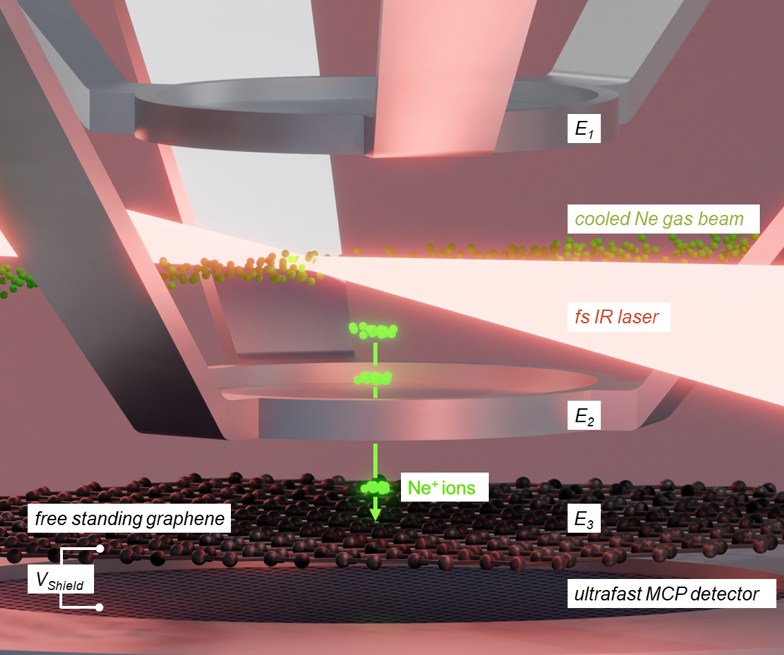
In addition, the front of the MCP can be biased with respect to the graphene target to de- and accelerate particles emitted from the graphene towards the detector. This allows for mass-spectrometry by a time-of-flight analysis as any potential applied to accelerate (decelerate) electrons will inherently result in the mass/charge-dependent deceleration (acceleration) of ions passing through the freestanding graphene target. The potential difference between the freestanding graphene and the MCP front is termed as VShield and if is lower than the kinetic energy Ekin of the ions, the resulting spectrum will include any emitted electrons and ions.
To measure the flight time of particles emitted from the graphene target, the output signal of the MCP is fed into an ultrafast oscilloscope (LeCroy WavePro404). The arrival time of each MCP pulse is measured against a signal of a fast photodiode which is triggered by a small fraction of the ionizing laser pulse. The time difference between the 50 % mark of the photodiode signal and 50 % mark of the MCP signal are recorded in a histogram resulting in the time-of-flight spectra seen in Fig. 6.
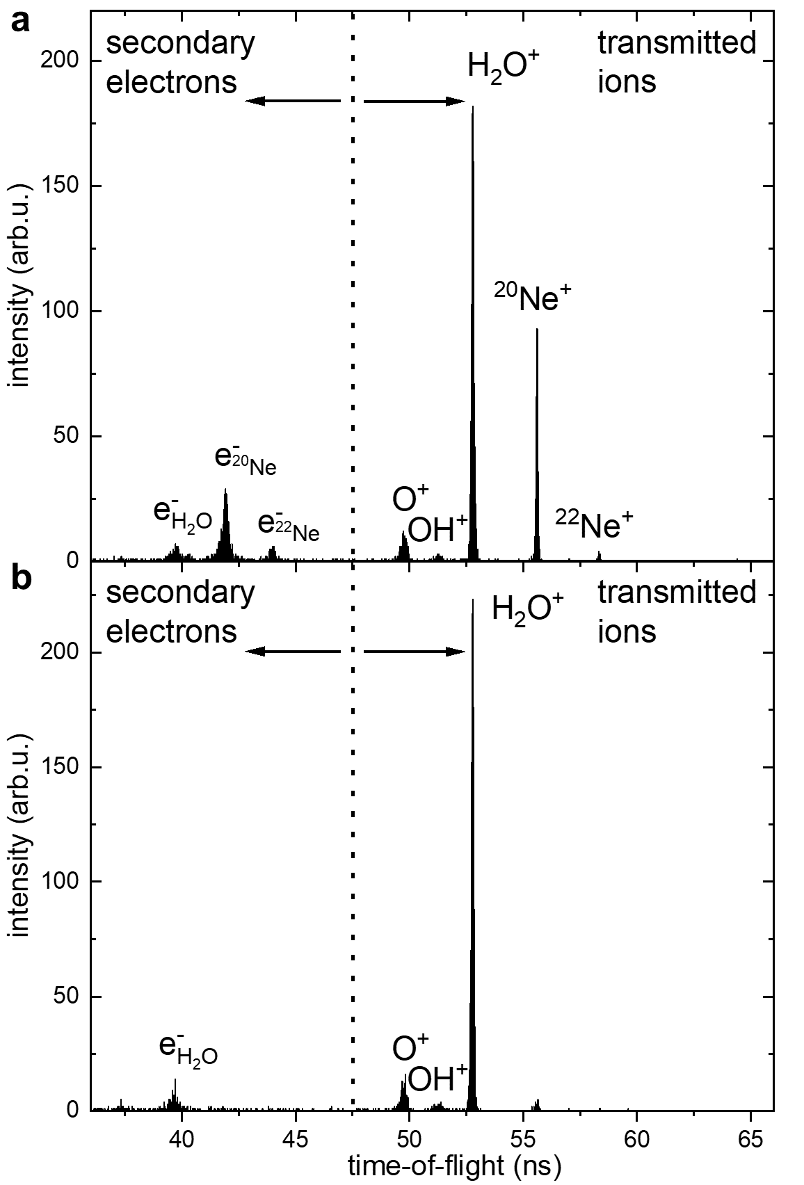
The spectrum shown in Fig. 6 a was collected from ions which were first accelerated to a kinetic energy of Ekin = 3.5 keV and then after passing through the graphene target decelerated by eVShield2.0 keV. Since the ions hit the MCP with a remaining energy of E = 1.5 keV, they still result in a detectable signal, making the transmitted ions observable. If the neon gas jet is on, as shown in Fig. 6 a, peaks become clearly visible in the spectrum, which we therefore attribute to 20Ne+ and its isotope 22Ne+. When the gas jet is turned off, see Fig. 6 b, the signal nearly vanishes (not completely as there is a small leakage of the nozzle producing the neon gas jet).
The arrival time of said signals can be converted to a mass-to-charge ratio, and with the assumption that the main signal indeed stems from 20Ne+ and 22Ne+, respectively, the ToF signal of other molecules and species can be determined. The signal at 52.7 ns can then be attributed to from the residual gas, and 49.7 ns correspond to O, as well as OH at 51.2 ns, stemming from fragmented due to the ionization process. Signals with even shorter arrival times can be explained by secondary electrons emitted by the graphene target after an ion impact. One indicator for this is that only certain peaks disappear when the neon jet is absent. Therefore these must result from the gas jet itself and can only be explained by secondary electrons emitted from the graphene target after an ion impact.
To calculate the electron yield we look at the total numbers of events which can be assigned to a secondary electron and the corresponding transmitted ion. For Ne+, we measure that 80 % of ions will lead to an emission of an electron. But due to the fact that electrons at 2.0 keV [51, 52] and ions at 1.5 keV [53] do not have the same detection efficiency, we over-estimate the total number of electrons and under-estimate the number of ions. This brings our results closer to the 0.5 electrons per ion that theoretical work by Yao et al. predicts [54].
IV Conclusion and outlook
In conclusion, we have demonstrated the manufacturing of samples with graphene triple layers spanning circular holes of 150 without the use of any polymer. Our method has a high coverage (90 %) and results in clean, flat, homogeneously doped and strained samples. Optical profilometry has in this context proven to be an efficient tool for rapid quality control, ensuring high throughput. By means of THz spectroscopy we could show that our samples feature a high charge carrier density and mobility. This together with the phonon modes confirm that the triple layer targets are structurally and electronically very similar to monolayer-graphene, facilitating the comparison of experimental data with theoretical predictions.
In addition, we have shown that our triple layer targets are efficient ion-to-electron converters and can be applied for ToF mass spectrometry. We find them easy to handle and to be sufficiently robust against irradiation damage. In comparison to previously used carbon foils they are ultrathin and their thickness is defined with an accuracy of ca. 1Å which makes them particularly interesting for fundamental studies in the field of ion-solid interaction. With respect to applications, our graphene samples could be used, e.g., to greatly improve the mass resolution of ToF spectrometers. Conventional set-ups use carbon foils to generate the START signal, the timing of which suffers from angular and energy straggling, which would be minimized or even absent (no collision cascade) in as-thin-as-it-gets films.
For this work, the overall dimensions of the targets has been specifically adapted to fit into our ps-ion source but the manufacturing process can be up-scaled to even larger hole substrates. Our method can be used to fabricate graphene targets for future pump-probe-experiments with ultrashort ion pulses but because of their good graphene/substrate area ratio of 58 %, they are also applicable for stripping purposes and any type of coincidence measurements. Due to their unique properties, we further expect our targets to be useful in other applications such as pressure sensors or in the field of NEMS and MEMS, respectively.
Acknowledgements.
The authors are greatly indebted to Ping Zhou for his assistance with the laser system. We thank the Deutsche Forschungsgemeinschaft (DFG) for their financial support of project C05 and B09 within the Collaborative Research Center (CRC) 1242 ‘Non-equilibrium dynamics in the time domain’ (project number 278162697) and the Federal Ministry of Education and Research (BMBF) for funding within project 05K16PG1.References
- Li and Zhou [2012] H. Li and H. Zhou, Enhancing the performances of Li-ion batteries by carbon-coating: present and future, Chemical Communications 48, 1201 (2012).
- Adeel et al. [2022] M. Adeel, K. Asif, V. Canzonieri, H. R. Barai, M. M. Rahman, S. Daniele, and F. Rizzolio, Controlled, partially exfoliated, self-supported functionalized flexible graphitic carbon foil for ultrasensitive detection of sars-cov-2 spike protein, Sensors and Actuators B: Chemical 359, 131591 (2022).
- Oliphant [1930] M. Oliphant, The liberation of electrons from metal surfaces by positive ions. part I.—experimental, Proceedings of the Royal Society of London. Series A, Containing Papers of a Mathematical and Physical Character 127, 373 (1930).
- Oliphant and Moon [1930] M. Oliphant and P. Moon, The liberation of electrons from metal surfaces by positive ions. part II.—theoretical, Proceedings of the Royal Society of London. Series A, Containing Papers of a Mathematical and Physical Character 127, 388 (1930).
- Ebert et al. [2014] R. W. Ebert, F. Allegrini, S. A. Fuselier, G. Nicolaou, P. Bedworth, S. Sinton, and K. J. Trattner, Angular scattering of 1-50 keV ions through graphene and thin carbon foils: potential applications for space plasma instrumentation, Review of Scientific Instruments 85, 033302 (2014).
- Allegrini et al. [2003] F. Allegrini, R. F. Wimmer-Schweingruber, P. Wurz, and P. Bochsler, Determination of low-energy ion-induced electron yields from thin carbon foils, Nuclear Instruments and Methods in Physics Research Section B: Beam Interactions with Materials and Atoms 211, 487 (2003).
- Allegrini et al. [2016] F. Allegrini, R. W. Ebert, and H. O. Funsten, Carbon foils for space plasma instrumentation, Journal of Geophysical Research: Space Physics 121, 3931 (2016).
- Vira et al. [2020] A. D. Vira, P. A. Fernandes, R. M. Skoug, H. O. Funsten, and D. B. Reisenfeld, Understanding mass resolution of foil–based time–of–flight mass spectrometry, Journal of Geophysical Research: Space Physics 125, e2020JA027971 (2020).
- Menendez et al. [1986] M. G. Menendez, M. M. Duncan, S. D. Berry, I. A. Sellin, W. Meckbach, P. Focke, and I. B. Nemirovsky, Coincidence experiment concerning the origin of convoy electrons produced by swift deuterium beams traversing carbon foils, Physical review. A, General physics 33, 2160 (1986).
- McComas and Nordholt [1990] D. J. McComas and J. E. Nordholt, New approach to 3-d, high sensitivity, high mass resolution space plasma composition measurements, Review of Scientific Instruments 61, 3095 (1990).
- Holeňák et al. [2021] R. Holeňák, S. Lohmann, F. Sekula, and D. Primetzhofer, Simultaneous assessment of energy, charge state and angular distribution for medium energy ions interacting with ultra-thin self-supporting targets: A time-of-flight approach, Vacuum 185, 109988 (2021).
- Moak [1976] C. D. Moak, Stripping in foils and gases, IEEE Transactions on Nuclear Science 23, 1126 (1976).
- Hattass et al. [1999] M. Hattass, T. Schenkel, A. V. Hamza, A. V. Barnes, M. W. Newman, J. W. McDonald, T. R. Niedermayr, G. A. Machicoane, and D. H. Schneider, Charge equilibration time of slow, highly charged ions in solids, Physical Review Letters 82, 4795 (1999).
- Meyer et al. [2007] J. C. Meyer, A. K. Geim, M. I. Katsnelson, K. S. Novoselov, T. J. Booth, and S. Roth, The structure of suspended graphene sheets, Nature 446, 60 (2007).
- Chen et al. [2016] Y.-M. Chen, S.-M. He, C.-H. Huang, C.-C. Huang, W.-P. Shih, C.-L. Chu, J. Kong, J. Li, and C.-Y. Su, Ultra-large suspended graphene as a highly elastic membrane for capacitive pressure sensors, Nanoscale 8, 3555 (2016).
- Rosłoń et al. [2020] I. E. Rosłoń, R. J. Dolleman, H. Licona, M. Lee, M. Šiškins, H. Lebius, L. Madauß, M. Schleberger, F. Alijani, H. S. J. van der Zant, and P. G. Steeneken, High-frequency gas effusion through nanopores in suspended graphene, Nature Communications 11, 6025 (2020).
- Carvalho et al. [2022] A. F. Carvalho, B. Kulyk, A. J. S. Fernandes, E. Fortunato, and F. M. Costa, A review on the applications of graphene in mechanical transduction, Advanced Materials 34, e2101326 (2022).
- Romijn et al. [2021] J. Romijn, R. J. Dolleman, M. Singh, H. S. J. van der Zant, P. G. Steeneken, P. M. Sarro, and S. Vollebregt, Multi-layer graphene pirani pressure sensors, Nanotechnology 32, 10.1088/1361-6528/abff8e (2021).
- Shin et al. [2023] D. H. Shin, H. Kim, S. H. Kim, H. Cheong, P. G. Steeneken, C. Joo, and S. W. Lee, Graphene nano-electromechanical mass sensor with high resolution at room temperature, iScience 26, 105958 (2023).
- Stoll and Kolmakov [2012] J. D. Stoll and A. Kolmakov, Electron transparent graphene windows for environmental scanning electron microscopy in liquids and dense gases, Nanotechnology 23, 505704 (2012).
- Leidinger et al. [2021] P. Leidinger, J. Kraus, T. Kratky, P. Zeller, T. O. Menteş, F. Genuzio, A. Locatelli, and S. Günther, Toward the perfect membrane material for environmental X-ray photoelectron spectroscopy, Journal of Physics D: Applied Physics 54, 234001 (2021).
- O’Hern et al. [2012] S. C. O’Hern, C. A. Stewart, M. S. H. Boutilier, J.-C. Idrobo, S. Bhaviripudi, S. K. Das, J. Kong, T. Laoui, M. Atieh, and R. Karnik, Selective molecular transport through intrinsic defects in a single layer of CVD graphene, ACS Nano 6, 10130 (2012).
- Koenig et al. [2012] S. P. Koenig, L. Wang, J. Pellegrino, and J. S. Bunch, Selective molecular sieving through porous graphene, Nature Nanotechnology 7, 728 (2012).
- Surwade et al. [2015] S. P. Surwade, S. N. Smirnov, I. V. Vlassiouk, R. R. Unocic, G. M. Veith, S. Dai, and S. M. Mahurin, Water desalination using nanoporous single-layer graphene, Nature Nanotechnology 10, 459 (2015).
- Madauß et al. [2017] L. Madauß, J. Schumacher, M. Ghosh, O. Ochedowski, J. Meyer, H. Lebius, B. Ban-d’Etat, M. E. Toimil-Molares, C. Trautmann, R. G. H. Lammertink, M. Ulbricht, and M. Schleberger, Fabrication of nanoporous graphene/polymer composite membranes, Nanoscale 9, 10487 (2017).
- Frank et al. [2007] I. W. Frank, D. M. Tanenbaum, A. M. van der Zande, and P. L. McEuen, Mechanical properties of suspended graphene sheets, Journal of Vacuum Science & Technology B: Microelectronics and Nanometer Structures Processing, Measurement, and Phenomena 25, 2558 (2007).
- Lee et al. [2008] C. Lee, X. Wei, J. W. Kysar, and J. Hone, Measurement of the elastic properties and intrinsic strength of monolayer graphene, Science (New York, N.Y.) 321, 385 (2008).
- Booth et al. [2008] T. J. Booth, P. Blake, R. R. Nair, Da Jiang, E. W. Hill, U. Bangert, A. Bleloch, M. Gass, K. S. Novoselov, M. I. Katsnelson, and A. K. Geim, Macroscopic graphene membranes and their extraordinary stiffness, Nano letters 8, 2442 (2008).
- Ochedowski et al. [2013] O. Ochedowski, K. Marinov, G. Wilbs, G. Keller, N. Scheuschner, D. Severin, M. Bender, J. Maultzsch, F. J. Tegude, and M. Schleberger, Radiation hardness of graphene and MoS2 field effect devices against swift heavy ion irradiation, Journal of Applied Physics 113, 10.1063/1.4808460 (2013).
- Kozubek et al. [2014] R. Kozubek, O. Ochedowski, I. Zagoranskiy, M. Karlušić, and M. Schleberger, Application of HOPG and CVD graphene as ion beam detectors, Nuclear Instruments and Methods in Physics Research Section B: Beam Interactions with Materials and Atoms 340, 81 (2014).
- Ernst et al. [2016] P. Ernst, R. Kozubek, L. Madauß, J. Sonntag, A. Lorke, and M. Schleberger, Irradiation of graphene field effect transistors with highly charged ions, Nuclear Instruments and Methods in Physics Research Section B: Beam Interactions with Materials and Atoms 382, 71 (2016).
- Gruber et al. [2016] E. Gruber, R. A. Wilhelm, R. Pétuya, V. Smejkal, R. Kozubek, A. Hierzenberger, B. C. Bayer, I. Aldazabal, A. K. Kazansky, F. Libisch, A. V. Krasheninnikov, M. Schleberger, S. Facsko, A. G. Borisov, A. Arnau, and F. Aumayr, Ultrafast electronic response of graphene to a strong and localized electric field, Nature Communications 7, 13948 (2016).
- Kuramitsu et al. [2022] Y. Kuramitsu, T. Minami, T. Hihara, K. Sakai, T. Nishimoto, S. Isayama, Y. T. Liao, K. T. Wu, W. Y. Woon, S. H. Chen, Y. L. Liu, S. M. He, C. Y. Su, M. Ota, S. Egashira, A. Morace, Y. Sakawa, Y. Abe, H. Habara, R. Kodama, L. N. K. Döhl, N. Woolsey, M. Koenig, H. S. Kumar, N. Ohnishi, M. Kanasaki, T. Asai, T. Yamauchi, K. Oda, K. Kondo, H. Kiriyama, and Y. Fukuda, Robustness of large-area suspended graphene under interaction with intense laser, Scientific Reports 12, 2346 (2022).
- Zan et al. [2012] R. Zan, Q. M. Ramasse, U. Bangert, and K. S. Novoselov, Graphene reknits its holes, Nano letters 12, 3936 (2012).
- Creutzburg et al. [2021] S. Creutzburg, A. Niggas, D. Weichselbaum, P. L. Grande, F. Aumayr, and R. A. Wilhelm, Angle-dependent charge exchange and energy loss of slow highly charged ions in freestanding graphene, Physical Review A 104, 10.1103/PhysRevA.104.042806 (2021).
- Tilmann et al. [2023] R. Tilmann, C. Bartlam, O. Hartwig, B. Tywoniuk, N. Dominik, C. P. Cullen, L. Peters, T. Stimpel-Lindner, N. McEvoy, and G. S. Duesberg, Identification of ubiquitously present polymeric adlayers on 2D transition metal dichalcogenides, ACS Nano 17, 10617 (2023).
- Madauß et al. [2020] L. Madauß, E. Pollmann, T. Foller, J. Schumacher, U. Hagemann, T. Heckhoff, M. Herder, L. Skopinski, L. Breuer, A. Hierzenberger, A. Wittmar, H. Lebius, A. Benyagoub, M. Ulbricht, R. Joshi, and M. Schleberger, A swift technique to hydrophobize graphene and increase its mechanical stability and charge carrier density, npj 2D Materials and Applications 4, 1 (2020).
- Huang et al. [2011] P. Y. Huang, C. S. Ruiz-Vargas, A. M. van der Zande, W. S. Whitney, M. P. Levendorf, J. W. keVek, S. Garg, J. S. Alden, C. J. Hustedt, Y. Zhu, J. Park, P. L. McEuen, and D. A. Muller, Grains and grain boundaries in single-layer graphene atomic patchwork quilts, Nature 469, 389 (2011).
- Baragiola et al. [1998] R. A. Baragiola, M. Shi, R. A. Vidal, and C. A. Dukes, Fast proton-induced electron emission from rare-gas solids and electrostatic charging effects, Physical Review B 58, 13212 (1998).
- Lee et al. [2012] J. E. Lee, G. Ahn, J. Shim, Y. S. Lee, and S. Ryu, Optical separation of mechanical strain from charge doping in graphene, Nature Communications 3, 1024 (2012).
- Kim and Ryu [2016] S. Kim and S. Ryu, Thickness-dependent native strain in graphene membranes visualized by raman spectroscopy, Carbon 100, 283 (2016).
- Nečas and Klapetek [2012] D. Nečas and P. Klapetek, Gwyddion: an open-source software for spm data analysis, Open Physics 10, 10.2478/s11534-011-0096-2 (2012).
- Lloyd-Hughes and Jeon [2012] J. Lloyd-Hughes and T.-I. Jeon, A review of the terahertz conductivity of bulk and nano-materials, Journal of Infrared, Millimeter, and Terahertz Waves 33, 871 (2012).
- Dawlaty et al. [2008] J. M. Dawlaty, S. Shivaraman, J. Strait, P. George, M. Chandrashekhar, F. Rana, M. G. Spencer, D. Veksler, and Y. Chen, Measurement of the optical absorption spectra of epitaxial graphene from terahertz to visible, Applied Physics Letters 93, 10.1063/1.2990753 (2008).
- Adam [2011] A. J. L. Adam, Review of near-field terahertz measurement methods and their applications, Journal of Infrared, Millimeter, and Terahertz Waves 32, 976 (2011).
- Glover and Tinkham [1957] R. E. Glover and M. Tinkham, Conductivity of superconducting films for photon energies between 0.3 and 40kTc, Physical Review 108, 243 (1957).
- Bolotin et al. [2008] K. I. Bolotin, K. J. Sikes, Z. Jiang, M. Klima, G. Fudenberg, J. Hone, P. Kim, and H. L. Stormer, Ultrahigh electron mobility in suspended graphene, Solid State Communications 146, 351 (2008).
- Golombek et al. [2021] A. Golombek, L. Breuer, L. Danzig, P. Kucharczyk, M. Schleberger, K. Sokolowski-Tinten, and A. Wucher, Generation of ultrashort keV ion pulses via femtosecond laser photoionization, New Journal of Physics 23, 033023 (2021).
- Kalkhoff et al. [2023] L. Kalkhoff, A. Golombek, M. Schleberger, K. Sokolowski-Tinten, A. Wucher, and L. Breuer, Path to ion-based pump-probe experiments: Generation of 18 picosecond keV Ne+ ion pulses from a cooled supersonic gas beam, Physical Review Research 5, 033106 (2023).
- Wiley and McLaren [1955] W. C. Wiley and I. H. McLaren, Time-of-flight mass spectrometer with improved resolution, Review of Scientific Instruments 26, 1150 (1955).
- Galanti et al. [1971] M. Galanti, R. Gott, and J. F. Renaud, A high resolution, high sensitivity channel plate image intensifier for use in particle spectrographs, Review of Scientific Instruments 42, 1818 (1971).
- Blase et al. [2017] R. C. Blase, R. R. Benke, G. P. Miller, K. S. Pickens, and J. H. Waite, Microchannel plate detector detection efficiency to monoenergetic electrons between 3 and 28 keV, Review of Scientific Instruments 88, 053302 (2017).
- Brehm et al. [1995] B. Brehm, J. Grosser, T. Ruscheinski, and M. Zimmer, Absolute detection efficiencies of a microchannel plate detector for ions, Measurement Science and Technology 6, 953 (1995).
- Y. Yao, A. Metzlaff, A. Wucher, M. Schleberger, L. Breuer, and A. Schleife [2023] Y. Yao, A. Metzlaff, A. Wucher, M. Schleberger, L. Breuer, and A. Schleife, Real-time electron emission dynamics of graphene under proton irradiation, arXiv (2023).
- Skopinski et al. [2023] L. Skopinski, S. Kretschmer, P. Ernst, M. Herder, L. Madauß, L. Breuer, A. V. Krasheninnikov, and M. Schleberger, Velocity distributions of particles sputtered from supported two-dimensional MoS2 during highly charged ion irradiation, Physical Review B 107, 075418 (2023).
- Creutzburg et al. [2020] S. Creutzburg, J. Schwestka, A. Niggas, H. Inani, M. Tripathi, A. George, R. Heller, R. Kozubek, L. Madauß, N. McEvoy, S. Facsko, J. Kotakoski, M. Schleberger, A. Turchanin, P. L. Grande, F. Aumayr, and R. A. Wilhelm, Vanishing influence of the band gap on the charge exchange of slow highly charged ions in freestanding single-layer MoS2, Physical Review B 102, 045408 (2020).