Shot noise-mitigated secondary electron imaging with ion count-aided microscopy
Abstract
Modern science is dependent on imaging on the nanoscale, often achieved through processes that detect secondary electrons created by a highly focused incident charged particle beam [1, 2]. Scanning electron microscopy is employed in applications such as critical-dimension metrology and inspection for semiconductor devices [3], materials characterization in geology [4], and examination of biological samples [5]. With its applicability to non-conducting materials (not requiring sample coating before imaging), helium ion microscopy (HIM) is especially useful in the high-resolution imaging of biological samples such as animal organs [6, 7], tumor cells [8], and viruses [9, 10]. However, multiple types of measurement noise limit the ultimate trade-off between image quality and the incident particle dose, which can preclude useful imaging of dose-sensitive samples. Existing methods to improve image quality do not fundamentally mitigate the noise sources [11, 12, 13, 14, 15, 16, 17]. Furthermore, barriers to assigning a physically meaningful scale make these modalities qualitative. Here we introduce ion count-aided microscopy (ICAM), which is a quantitative imaging technique that uses statistically principled estimation of the secondary electron yield. With a readily implemented change in data collection, ICAM nearly eliminates the influence of source shot noise—the random variation in the number of incident ions in a fixed time duration. In HIM, we demonstrate 3 dose reduction; based on a good match between these empirical results and theoretical performance predictions, the dose reduction factor is larger when the secondary electron yield is higher. ICAM thus facilitates imaging of fragile samples and may make imaging with heavier particles more attractive.
In secondary electron imaging (SEI), a beam of charged particles (electrons or ions) is raster scanned across the sample being imaged. At each scan location, the incident beam is held in place while it excites secondary electrons (SEs) that are detected by a secondary electron detector (SED). A detected signal intensity is converted to a pixel brightness value. Scanning over a rectangular grid forms the final image of the sample. The ideal SE image would be a map of the sample’s SE yield , i.e., the mean number of SEs generated per incident particle. However, since SEDs do not have sufficient energy resolution to count SEs, and the gain and efficiency of the detector are generally unknown to the user, conventional SE images are merely qualitative—they cannot be directly mapped to pixelwise SE yields.
The quality of SEI is affected by three sources of noise: random variation in the number of incident particles (source shot noise), in the number of emitted SEs for each incident particle (target shot noise), and in the signal produced by the SED in response to SEs (detector noise). These noise sources limit the image quality achievable in SEI at any given imaging dose. For rugged materials such as gold or copper, the image quality can be improved by increasing dose. However, for fragile, radiation-sensitive materials, increase in dose also increases the damage imparted during imaging. This type of damage is especially significant for HIM as compared to SEM because of the greater mass of helium ions.
One approach to improving the quality of SEI has been the implementation of digital SE count imaging using the inherent pulse counting capabilities of the SED [18, 19, 20]. While this technique improves imaging signal-to-noise-ratio at low SE yields, it cannot be directly applied at higher yields where multiple SEs may be detected simultaneously. Post-processing methods to reduce noise, such as Gaussian/Poisson deconvolution [11, 12], compressed sensing [13, 14, 15], inpainting [16], and adaptive scanning [17], rely on assumptions about the underlying image structure rather than on the statistics of the particle source or SE emission. Where applicable, these types of post-processing can be combined with more fundamental physics-based improvements.
In this work, we introduce ion count-aided microscopy (ICAM), which uses novel data processing to nearly eliminate source shot noise. The target shot noise is inherent to the measured beam–sample interactions, and the detector noise can be reduced by altering the choice of detector technology; thus, ICAM approaches the accuracy limits of SEI. We demonstrate ICAM with a helium ion microscope to achieve quantitative, nanoscale SE yield metrology. Building upon a time-resolved measurement concept developed under an assumption of perfect SE observation [21, 22, 23], we use the full waveform of the SED signal to infer ion incidence events. Using the number of observed ion incidence events improves SE yield estimation significantly; we demonstrate reduction of the dose required for a given image quality by up to a factor of 3. Theoretical analysis suggests that the dose reduction factor provided by ICAM is approximately equal to the SE yield and thus can be much larger for other incident particles and samples [24].
Data collection to allow incident ion counting
Figure 1 shows a schematic of our imaging setup. We used a Zeiss Orion Plus helium ion microscope operated at 30 beam energy in our experiments. We outcoupled both the SED and the beam scan signals into a 12-bit, 100 MHz digitizer (Gage RazorExpress 1642), which sampled both signals at . Figure 1 shows a snapshot of the SED voltage signal. The SED is typically an Everhart–Thornley detector [25], which consists of a scintillator followed by a photomultiplier. The signal generated by the SED consists of a series of voltage pulses of varying heights, where each pulse corresponds to a burst of detected SEs [26]. The mean full width at half maximum (FWHM) of the pulses is [27]. In our experiments we used a beam current (measured with a picoammeter connected to a Faraday cup), which was low enough to make pulse pile-up effects manageable.
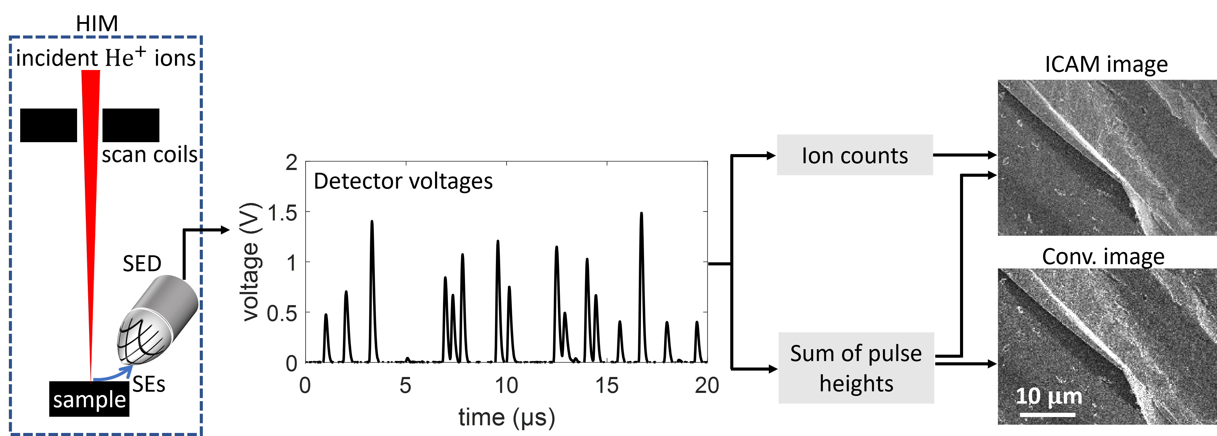
To create images, we collected the SED voltage and beam scan signals at pixel dwell times varying between and for a 512 512-pixel image. These settings correspond to an incident dose between 1.4 and 22 ions per pixel, where is the elementary charge. The maximum image size and dwell time were set by the available memory of the digitizer. Next, using custom MATLAB scripts [28], we extracted the SED voltage pulse heights and the number of pulses for each pixel. Neglecting pulse pile-up, would be the number of incident ions that produced one or more detected SEs. To account for pile-up, we divide the raw value of by a correction factor that accounts for the probability of pulse overlap to yield a value [see Methods].
Secondary electron yield estimation
We used the measurements to create two pixelwise maps of : conventional, which models typical SEI; and ion count-aided (ICA), which implements our source shot noise-mitigated estimator. While typical SEI uses only , the performance of ICAM demonstrates the value of using as well.
From its definition as the number of SEs generated per incident particle, it is natural for an estimate of SE yield to be framed as
| (1) |
In bulk estimates of SE yield, measurements of the beam and sample currents may be used to calculate the numerator and denominator of this expression [29]. Our nanoscale mapping of uses this intuitive expression with numerator and denominator estimated from , .
Estimating number of SEs. If we knew the mean voltage produced by the detector in response to one SE, would be an unbiased estimator for the number of SEs. As detailed in figs. S1, S2, and S3, we found that a linear probabilistic model accurately describes the statistics of the SE pulses. In this model, the number of incident particles and the number of emitted SEs both follow Poisson distributions, and the response of the detector to one SE follows a Gaussian distribution. By fitting this model to the pulse height distributions from samples with different , we computed for the microscope imaging settings used. We also computed the standard deviation of the detector’s voltage response to one SE, . We used the estimate in the numerator of eq. 1 for both the conventional and ICA estimators.
Estimating number of incident particles. Conventionally, any estimate of the number of incident particles could depend only on the dose per pixel , since the number of discernible incidence events is not counted. In that case, since the model specifies , the value of itself is the best estimate of . In our method, we estimate using the count of ions that produced at least one SE, , corrected for pulse-pileup effects. Under our standard statistical assumptions, . The term optimally accounts for cases of 0 SE detection and can be a significant fraction of ( at , on average). Using this expression as an estimate of lowers the variance of the denominator of eq. 1 by a factor of [see Supplementary Information].
Combining these observations, we can write the expressions for the conventional () and ion count-assisted (ICA, ) estimators:
| (2) |
and
| (3) |
Note that the second of these is not a formula to evaluate but rather an equation to solve computationally. Figures S5 and S6 show theoretical and experimental calculations of the variance for both estimators, demonstrating the reduction in imaging noise possible with our improved estimate of . We also show in Figures S7 and S8 that the images produced by the conventional estimator are equivalent to those produced by the microscope software with suitable scaling.
Images with reduced source shot noise
Figure 2 shows comparisons between conventional and ICAM images of a scratch on a silicon chip at doses of , , and ions per pixel. All images have pixels and a horizontal field-of-view. These images are SE yield maps; instead of an arbitrary scale, gray-scale values correspond to physically meaningful values of as indicated by the colorbar. We can see that for each dose, the ICAM images appear less noisy than the conventional images due to source shot noise mitigation. The ICAM image at a dose of 8.2 ions/pixel (Figure 2B2) appears visually similar to the conventional image at a dose of 22 ions/pixel (Figure 2A3). Figure 2C is a plot of the standard deviation measured over all the pixels as a function of the imaging dose for the conventional ( ) and ICAM ( ) images. In addition to the three imaging noise components (source shot noise, target shot noise, and detector noise), this standard deviation has a contribution from variations in the features in the sample. As the dose increases, we expect all three imaging noise components to reduce, so at high doses the standard deviation should asymptotically approach the inherent feature standard deviation. This is the behavior we observe in Figure 2C. At low doses, both the conventional and ICAM standard deviations vary inversely with the dose (straight line on a log-log plot), and they show saturation at higher doses. The horizontal gaps marked in Figure 2C indicate that ICAM images have the same standard deviations as conventional images at 2- to 3-times the dose, and the doses selected for Figure 2A and B illustrate this as well.
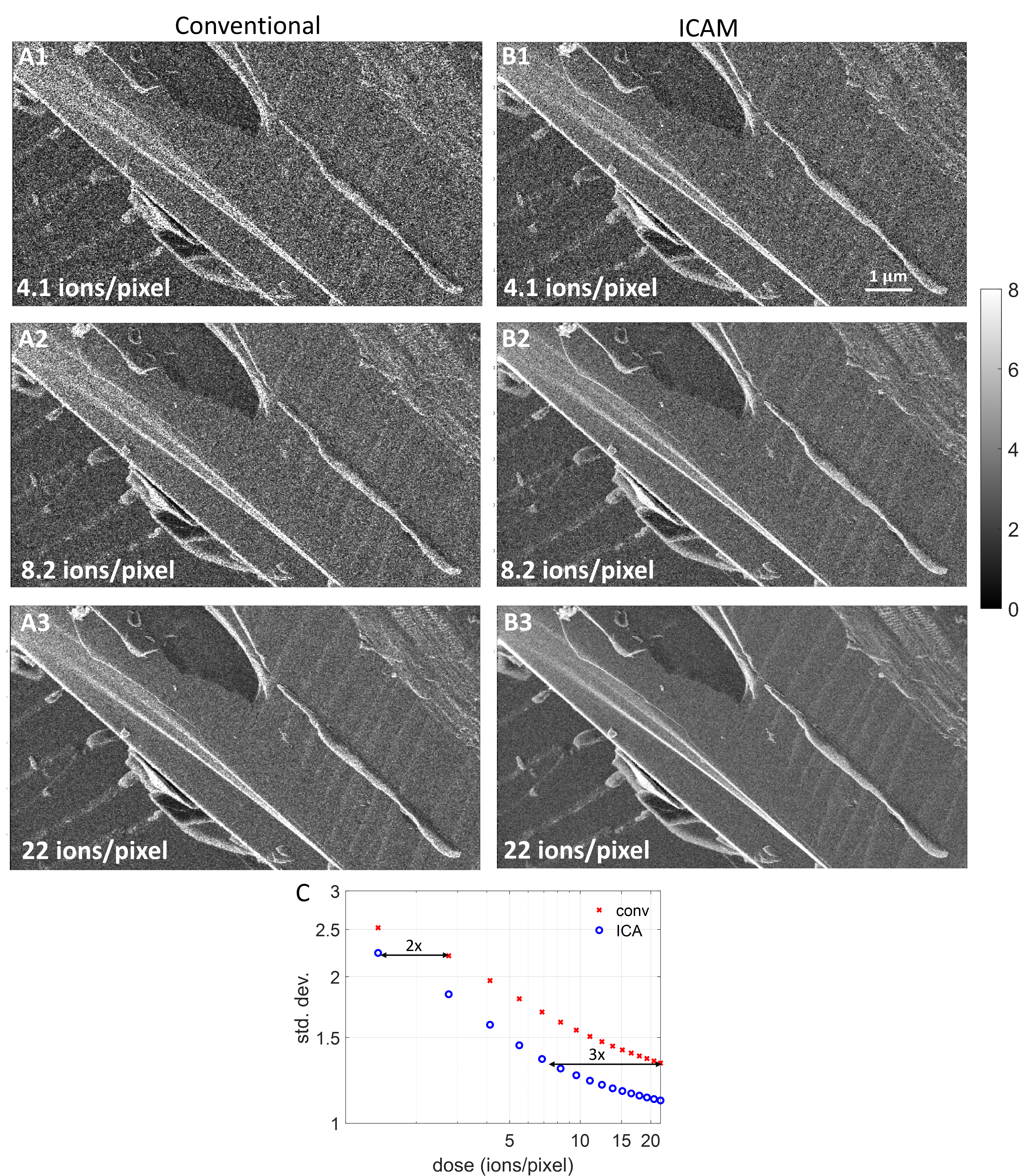
Further evidence of the reduction in noise is provided by a calculation of Thong’s signal-to-noise ratio (SNR) for both images [30]. This metric aims to calculate SNR for a single SEM image (without knowledge of ground truth) by separating the contributions of signal and noise to the image’s autocorrelation. We calculated this SNR to be 5.6 for the ICAM image and 2.8 for the conventional image at . Figure S9 presents a calculation of imaging resolution using Fourier ring correlation [31, 32, 33, 34] at the threshold [35, 36] for both images; the ICAM image shows a 21% improvement in resolution.
Figure 3, A and B, shows the conventional and ICAM images of a patterned silicon substrate with gold squares. The ICAM image again appears to be smoother and less noisy than the conventional image, especially in the brighter regions that correspond to gold. The lower noise in the ICAM image is also reflected in Thong’s SNR: the ICAM image has an SNR of 2.12, while the conventional image has an SNR of 1.61.
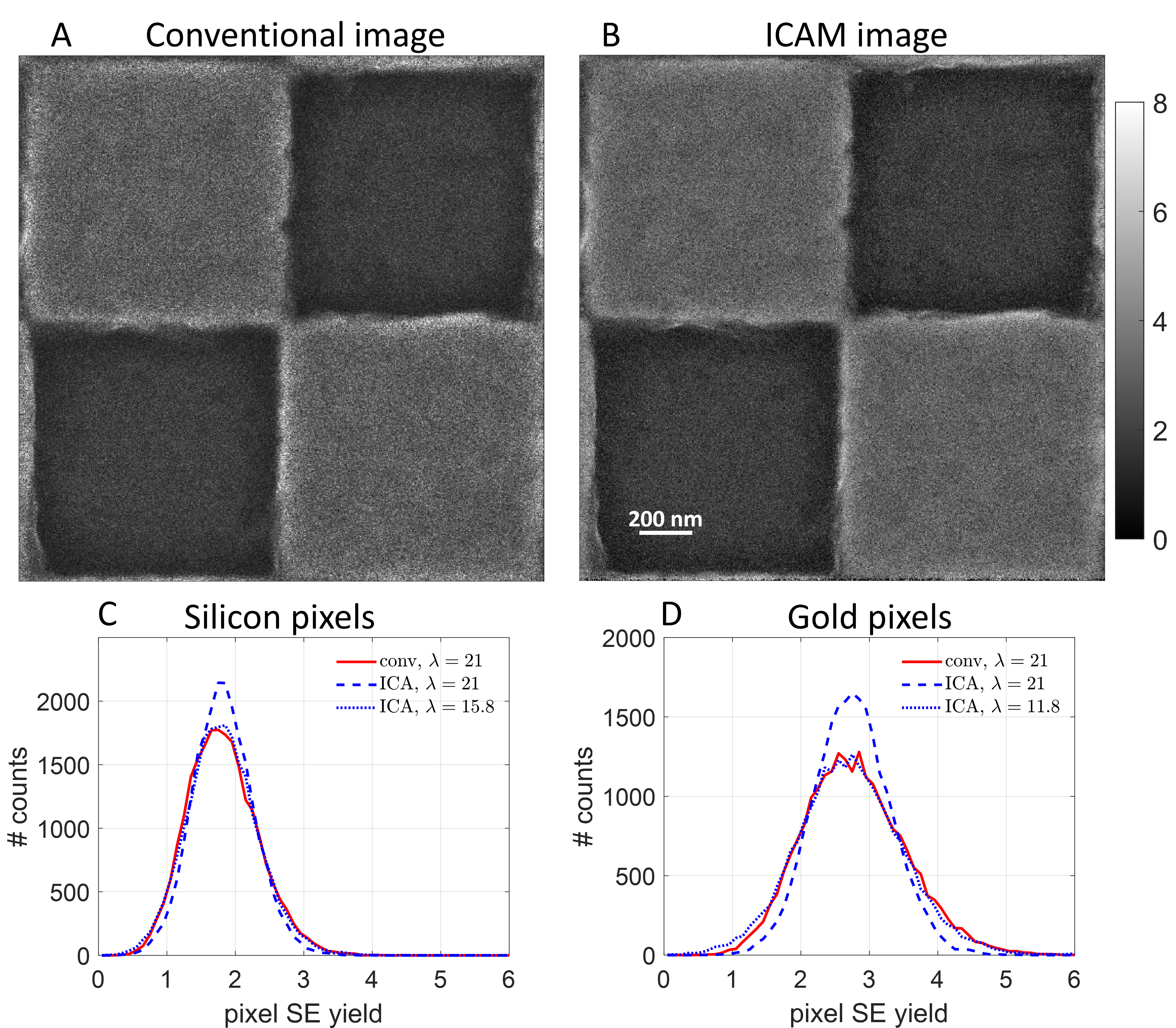
Since this sample has two types of pixels, it provides a good platform for further numerical characterization of the advantages of ICA estimation. Figure 3, C and D, are image histograms with bin width 0.1 for two subsets of pixels in this sample—the darker, silicon pixels, and the brighter, gold pixels—at the same imaging dose. The histograms plot the frequency of occurrence of different pixel SE yields. Figure 3C shows the conventional and ICAM histogram for the dark (silicon) pixels, and Figure 3D for the bright (gold) pixels. For the silicon pixels, we measured a mean SE yield of 1.82. We can see that the histogram for the ICAM image is narrower than that for the conventional image at the same dose of . The width of the ICAM histogram at a lower dose of is comparable to that conventional image histogram. In other words, comparable image quality was attained using the ICA estimator at a dose that was lower than that for the conventional estimator by a factor of 1.33. For the gold pixels, we measured a mean SE yield of 2.75. The dose improvement factor in this case was 1.78.
Theoretical predictions
The reduction in imaging noise in Figures 2 and 3 agrees with Monte Carlo performance predictions computed from our model of the imaging process. Figure 4, A and B, compares the theoretical standard deviation as a function of dose with the experimental values we measured for the silicon and gold pixels in Figure 3, for both conventional and ICA estimators. Unlike the plots in Figure 2C, we expect no saturation since each square in Figure 3 is almost featureless; this is exactly what we observe in Figure 4, A and B. The experimental standard deviations agree closely with the theoretical values for all doses. We also see a bigger gap between the standard deviations of conventional and ICAM images at higher SE yield, as expected from the histograms in Figure 3, C and D. As SE yield rises, an increasing fraction of incident particles produce detected SEs, making the estimate of in eq. 3 more accurate and improving source shot noise mitigation by the ICAM estimator.
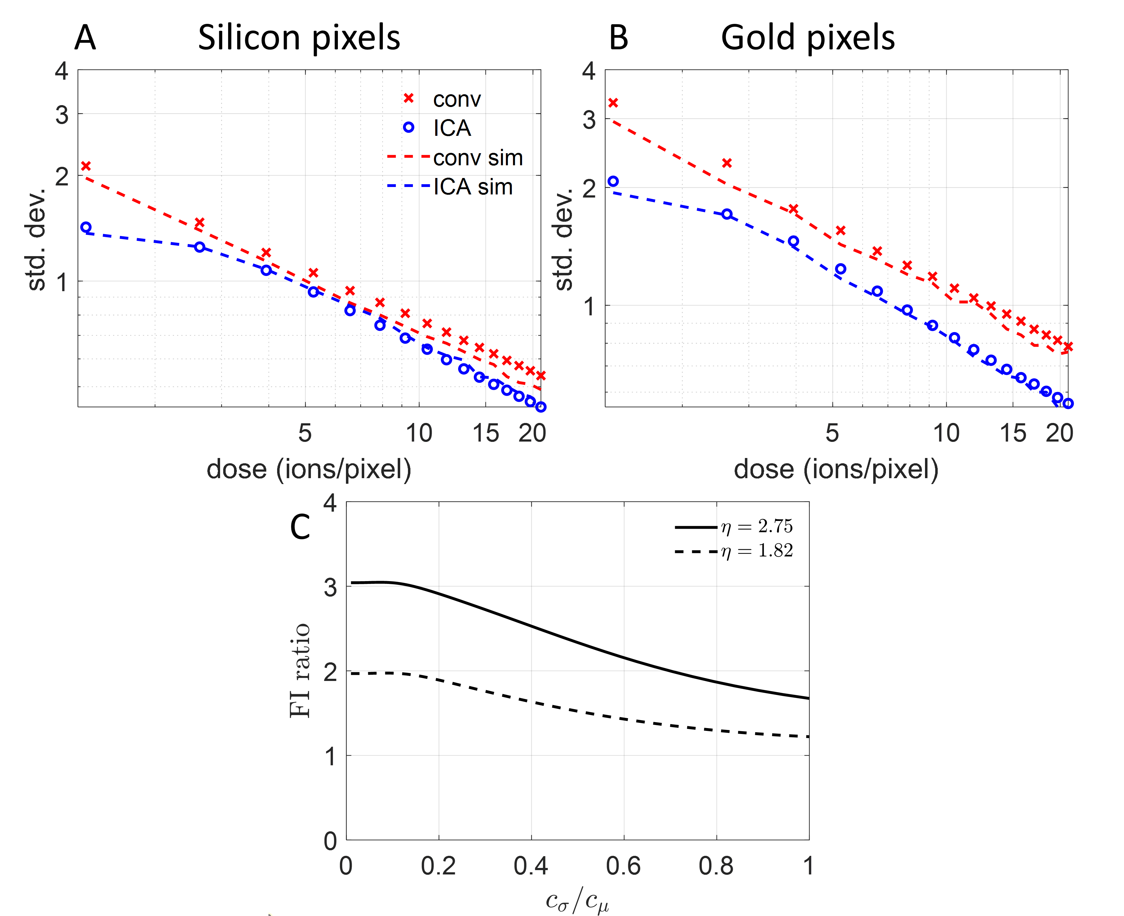
The experiments and performance predictions from simulations are consistent with theoretical analysis through Fisher information (FI). FI is a measure of the sensitivity of noisy data to the parameter to be estimated; higher FI indicates proportionately lower imaging noise. Figure 4C shows the ratio between the FI from ICAM and conventional measurement at as a function of , the standard deviation of the contribution of one SE normalized by its mean, for (solid black curve) and (dashed black curve). The ratio is a measure of the non-ideality of the SED—the larger this ratio, the more the SED deviates from ideal SE counting. As approaches zero, the FI ratio is simply , a strictly increasing and approximately linear function of [22]. We can see that the ratio of the FIs of ICAM and conventional measurement is greater than 1 for the entire range of , suggesting that ICAM images remain less noisy even for highly non-ideal detectors.
The non-ideality of the detector contributes additional noise to the image, leading to degradation in the FI ratio with increasing . For our system , and at this value we get FI ratios of about for and for . Due to the additive property of Fisher information, we consequently expect a dose reduction by a factor of at and at . These numbers are close to the experimental dose reductions we obtained for the sample in Figure 3.
The SE yield values we report here are not absolute, but are implicitly multiplied by the SED’s detection quantum efficiency (DQE) [37]. We measured the DQE to be about [see Supplementary Information]. Therefore, all SE yield values quoted here should be divided by this number for absolute SE yields. For example, the DQE-corrected mean SE yield for the sample in Figure 2 is 3.62, which is in agreement with theoretical predictions of the He-ion SE yield for silicon at [38].
Conventional estimates of SE yield require precise measurement of beam current. We observed that the beam current value measured by the picoammeter fluctuated by up to 10% for the same nominal setting of . As seen in eq. 2, the conventional estimate is inversely proportional to . Therefore, a 10% uncertainty in the value of the beam current results in a 10% uncertainty in . In contrast, the ICAM SE yield measurement is much less sensitive to precise knowledge of because it uses the observed count of ions in addition to knowledge of to estimate as seen in eq. 3. At , a 10% variation in causes 0.8% variation in [see Supplementary Information]. This reduced sensitivity to precise knowledge of the beam current could be used for removal of stripe artifacts that result from beam current variations [39].
Discussion and outlook
Ion count-aided microscopy differs from other techniques for image denoising and dose reduction in secondary electron imaging. Popular methods include image filtering deconvolution [11, 12, 40, 41], adaptive scanning [17], and sparse scanning and inpainting [14, 15, 16]. These methods do not attempt to model the SE generation and detection statistically, and they work as post-processing after conventional SE image generation. The ICAM method introduced here is based on statistical modelling of the SE detection process to improve initial image formation, and it can be combined with various types of post-processing.
Electron count imaging from scintillator-photomultiplier-based detectors has also been demonstrated to increase image SNR and temporal resolution in scanning transmission electron microscopy [42, 43, 44]. In this case, incident electrons that get scattered as they travel through the sample are detected. Therefore, at low beam currents, each detected pulse corresponds to one electron, similar to the case of high-energy SEM. These count-resolved methods are currently limited by pulse pile-up at higher beam currents. Since the distribution of heights of piled-up single electron pulses would be identical to that of a single multi-electron pulse, the methods presented here could be applied to model pile-up in these systems to further improve image SNR.
As shown in Figure 3, the reduction in noise with the ICA estimator increases with increasing SE yield. In fig. S6B, we present theoretical calculations of the variance for between 0 and 3.5, and we notice that noise reduction only occurs above an SE yield of about 1. This limitation would make our method less applicable to SEM at energies above . However, these estimators could still be used for low-voltage SEM, where SE yields can be high [45, 46]. Imaging with heavier ions, such as neon [47], would also increase SE yield over helium and consequently produce lower-noise images [see Supplementary Information]. Further, these techniques could also be used for secondary ion imaging and mass spectroscopy with helium and neon beams due to the high sputtering yield [48].
As shown in Figure 4C, the ratio of FI of ICAM and conventional imaging reduces with increasing , i.e., increasing variance in the detector’s response to each SE single SEs. Though the large value of that is typical for Everhart–Thornley detectors limits the performance of ICAM imaging, we were still able to demonstrate a significant improvement. Reduction in the variance of the SED’s response, by, for example, implementation of solid-state SE detectors [49], would improve both conventional and ICAM imaging while increasing the improvement factor of ICAM.
Acknowledgments
He Ion Microscope imaging was performed at the Laboratory for Surface Modification (LSM), a center within the School of Arts and Sciences, Rutgers University. Helpful discussions with Dr. Hussein Hijazi and Prof. Sylvie Rangan, Rutgers University; and Dr. Ben Caplins, National Institute of Standards and Technology, are gratefully acknowledged.
Competing interests
Schultz/Ionwerks owns patents on secondary electron detector designs and methods of use in correlated SE imaging and ion scattering time of flight measurements.
References
- [1] L. Reimer, Scanning Electron Microscopy, ch. Introduction, pp. 1–12. Berlin, Heidelberg: Springer-Verlag, 2nd ed., 1998.
- [2] B. W. Ward, J. A. Notte, and N. P. Economou, “Helium ion microscope: A new tool for nanoscale microscopy and metrology,” J. Vacuum Sci. Technol. B, vol. 24, pp. 2871–2874, Nov. 2006.
- [3] M. Postek and A. Vladar, Handbook of Silicon Semiconductor Metrology, ch. Critical Dimension Metrology in the Scanning Electron Microscope. Boca Raton: CRC Press, 2001.
- [4] S. J. B. Reed, Electron Microprobe Analysis and Scanning Electron Microscopy in Geology. Cambridge University Press, 2 ed., 2005.
- [5] S. Thiberge, A. Nechushtan, D. Sprinzak, O. Gileadi, V. Behar, O. Zik, Y. Chowers, S. Michaeli, J. Schlessinger, and E. Moses, “Scanning electron microscopy of cells and tissues under fully hydrated conditions,” Proceedings of the National Academy of Sciences, vol. 101, no. 10, pp. 3346–3351, 2004.
- [6] S. A. Boden, A. Asadollahbaik, H. N. Rutt, and D. M. Bagnall, “Helium ion microscopy of lepidoptera scales,” Scanning, vol. 34, no. 2, pp. 107–120, 2012.
- [7] W. L. Rice, A. N. Van Hoek, T. G. Păunescu, C. Huynh, B. Goetze, B. Singh, L. Scipioni, L. A. Stern, and D. Brown, “High resolution helium ion scanning microscopy of the rat kidney,” PLOS ONE, vol. 8, pp. 1–9, Mar. 2013.
- [8] D. Bazou, B. G., C. Reid, J. Boland, and H. Zhang, “Imaging of human colon cancer cells using he-ion scanning microscopy,” J. Microscopy, vol. 242, no. 3, pp. 290–294, 2011.
- [9] M. Leppänen, L.-R. Sundberg, E. Laanto, G. M. de Freitas Almeida, P. Papponen, and I. J. Maasilta, “Imaging bacterial colonies and phage–bacterium interaction at sub-nanometer resolution using helium-ion microscopy,” Advanced Biosystems, vol. 1, p. 1700070, Aug. 2017.
- [10] A. Merolli, L. Kasaei, S. Ramasamy, A. Kolloli, R. Kumar, S. Subbian, and L. C. Feldman, “An intra-cytoplasmic route for SARS-CoV-2 transmission unveiled by helium-ion microscopy,” Scientific Reports, vol. 12, Dec. 2022.
- [11] J. Roels, J. Aelterman, J. De Vylder, H. Luong, Y. Saeys, and W. Philips, “Bayesian deconvolution of scanning electron microscopy images using point-spread function estimation and non-local regularization,” in Proc. Ann. Int. Conf. IEEE Engineering in Medicine and Biology Society, (Orlando, FL), pp. 443–447, Aug. 2016.
- [12] W. E. Vanderlinde and J. N. Caron, “Blind deconvolution of SEM images,” in Proc. 33rd Int. Symp. Testing and Failure Analysis, pp. 97–102, Nov. 2007.
- [13] H. S. Anderson, J. Ilic-Helms, B. Rohrer, J. Wheeler, and K. Larson, “Sparse imaging for fast electron microscopy,” in Proc. SPIE Computational Imaging XI, vol. 8657, (Burlingame, CA), p. 86570C, Feb. 2013.
- [14] L. Kovarik, A. Stevens, A. Liyu, and N. D. Browning, “Implementing an accurate and rapid sparse sampling approach for low-dose atomic resolution STEM imaging,” Applied Physics Letters, vol. 109, p. 164102, 2016.
- [15] A. Stevens, L. Luzi, H. Yang, L. Kovarik, B. L. Mehdi, A. Liyu, M. E. Gehm, and N. D. Browning, “A sub-sampled approach to extremely low-dose STEM,” Applied Physics Letters, vol. 112, p. 043104, 2018.
- [16] S. Pang, X. Zhang, H. Li, and Y. Lu, “Edge determination improvement of scanning electron microscope images by inpainting and anisotropic diffusion for measurement and analysis of microstructures,” Measurement, vol. 176, p. 109217, 2021.
- [17] T. Dahmen, M. Engstler, C. Pauly, P. Trampert, N. de Jonge, F. Mücklich, and P. Slusallek, “Feature adaptive sampling for scanning electron microscopy,” Scientific Reports, vol. 6, p. 25350, July 2016.
- [18] D. C. Joy, “Noise and its effects on the low-voltage SEM,” in Biological Low-Voltage Scanning Electron Microscopy (H. Schatten and J. B. Pawley, eds.), pp. 129–144, New York, NY: Springer, 2008.
- [19] Y. Uchikawa, K. Gouhara, S. Yamada, T. Ito, T. Kodama, and P. Sardeshmukh, “Comparative study of electron counting and conventional analogue detection of secondary electrons in SEM,” J. Electron Microscopy, vol. 41, pp. 253–260, 1992.
- [20] A. Agarwal, J. Simonaitis, V. K. Goyal, and K. K. Berggren, “Secondary electron count imaging in SEM,” Ultramicroscopy, vol. 254, no. 113662, 2023.
- [21] M. Peng, J. Murray-Bruce, K. K. Berggren, and V. K. Goyal, “Source shot noise mitigation in focused ion beam microscopy by time-resolved measurement,” Ultramicroscopy, vol. 211, Apr. 2020.
- [22] M. Peng, J. Murray-Bruce, and V. K. Goyal, “Time-resolved focused ion beam microscopy: Modeling, estimation methods, and analyses,” IEEE Trans. Comput. Imaging, vol. 7, pp. 547–561, 2021.
- [23] A. Agarwal, M. Peng, and V. K. Goyal, “Continuous-time modeling and analysis of particle beam metrology,” IEEE J. Sel. Areas Inform. Theory, vol. 4, pp. 61–74, 2023.
- [24] U. Fehn, “Variance of ion-electron coefficients with atomic number of impacting ions,” International Journal of Mass Spectrometry and Ion Physics, vol. 21, no. 1, pp. 1–14, 1976.
- [25] T. E. Everhart and R. F. Thornley, “Wide-band detector for micro-microampere low-energy electron currents,” J. Scientific Instruments, vol. 37, pp. 246–248, 1960.
- [26] L. Novák and I. Müllerová, “Single electron response of the scintillator-light guide-photomultiplier detector,” J. Microscopy, vol. 233, pp. 76–83, 2009.
- [27] A. Agarwal, J. Simonaitis, and K. K. Berggren, “Image-histogram-based secondary electron counting to evaluate detective quantum efficiency in SEM,” Ultramicroscopy, vol. 224, p. 113238, 2021.
- [28] A. Agarwal and X. He, “Code for ion count-aided microscopy.” will be publicly released by Goyal-STIR-Group GitHub organization and assigned a DOI by Zenodo upon acceptance of paper, 2023.
- [29] H. Seiler, “Secondary electron emission in the scanning electron microscope,” J. Appl. Phys., vol. 54, p. R1, 1983.
- [30] J. T. L. Thong, K. S. Sim, and J. C. H. Phang, “Single-image signal-to-noise ratio estimation,” Scanning, vol. 23, pp. 328–336, 2001.
- [31] W. O. Saxton, “Basic software for digital image handling - reprinted from advances in electronics and electron physics, supplement 10, 1978.,” in Computer Techniques for Image Processing in Electron Microscopy (M. Hÿtch and P. W. Hawkes, eds.), vol. 214 of Advances in Imaging and Electron Physics, pp. 199–266, Amsterdam: Elsevier, 2020.
- [32] M. van Heel, W. Keegstra, W. Schutter, and E. F. J. van Bruggen, “Arthropod hemocyanin structures studied by image analysis,” Life Chemistry Reports, Suppl. 1, “The Structure and Function of Invertebrate Respiratory Proteins”’, EMBO workshop, pp. 69–72, 1982.
- [33] W. O. Saxton and W. Baumeister, “The correlation averaging of a regularly arranged bacterial cell envelope protein,” J. Microscopy, vol. 127, pp. 127–138, 1982.
- [34] M. van Heel, “Similarity measures between images,” Ultramicroscopy, vol. 21, pp. 95–100, 1987.
- [35] P. B. Rosenthal and R. Henderson, “Optimal determination of particle orientation, absolute hand, and contrast loss in single-particle electron cryomicroscopy,” J. Molecular Biology, vol. 333, pp. 721–745, Oct. 2003.
- [36] C. Sorzano, J. Vargas, J. Otón, V. Abrishami, J. de la Rosa-Trevín, J. Gómez-Blanco, J. Vilas, R. Marabini, and J. Carazo, “A review of resolution measures and related aspects in 3d electron microscopy,” Progress in Biophysics and Molecular Biology, vol. 124, pp. 1–30, Mar. 2017.
- [37] D. C. Joy, C. S. Joy, and R. D. Bunn, “Measuring the performance of scanning electron microscope detectors,” Scanning, vol. 18, pp. 533–538, 1996.
- [38] T. Yamanaka, K. Inai, K. Ohya, and T. Ishitani, “Simulation of secondary electron emission in helium ion microscope for overcut and undercut line-edge patterns,” in Proc. SPIE Metrology, Inspection, and Process Control for Microlithography XXIII, vol. 7272, p. 72722L, 2009.
- [39] S. W. Seidel, L. Watkins, M. Peng, A. Agarwal, C. Yu, and V. K. Goyal, “Online beam current estimation in particle beam microscopy,” IEEE Trans. Comput. Imaging, vol. 8, pp. 521–535, 2022.
- [40] J. Roels, F. Vernaillen, A. Kremer, A. Gonçalves, J. Aelterman, H. Q. Luong, B. Goossens, W. Philips, S. Lippens, and Y. Saeys, “An interactive ImageJ plugin for semi-automated image denoising in electron microscopy,” Nat. Commun., vol. 11, Dec. 2020.
- [41] D. Li, R. Guo, S.-Y. Lee, J. Choi, S.-B. Kim, S.-H. Park, I.-K. Shin, and C.-U. Jeon, “Noise filtering for accurate measurement of line edge roughness and critical dimension from sem images,” J. Vacuum Science & Technology B, Nanotechnology and Microelectronics: Materials, Processing, Measurement, and Phenomena, vol. 34, Nov. 2016.
- [42] X. Sang and J. M. Lebeau, “Characterizing the response of a scintillator-based detector to single electrons,” Ultramicroscopy, vol. 161, pp. 3–9, 2016.
- [43] A. Mittelberger, C. Kramberger, and J. C. Meyer, “Software electron counting for low-dose scanning transmission electron microscopy,” Ultramicroscopy, vol. 188, pp. 1–7, 2018.
- [44] J. J. P. Peters, T. Mullarkey, E. Hedley, K. H. Müller, A. Porter, A. Mostaed, and L. Jones, “Electron counting detectors in scanning transmission electron microscopy via hardware signal processing,” Nat. Commun., vol. 14, p. 5184, Aug. 2023.
- [45] D. C. Joy and C. S. Joy, “Low voltage scanning electron microscopy,” Micron, vol. 27, no. 3, pp. 247–263, 1996.
- [46] D. C. Joy, “A database on electron-solid interactions,” Scanning, vol. 17, pp. 270–275, Dec. 2006.
- [47] F. H. M. Rahman, S. McVey, L. Farkas, J. A. Notte, S. Tan, and R. H. Livengood, “The prospects of a subnanometer focused neon ion beam,” Scanning, vol. 34, pp. 129–134, July 2011.
- [48] T. Wirtz, N. Vanhove, L. Pillatsch, D. Dowsett, S. Sijbrandij, and J. Notte, “Towards secondary ion mass spectrometry on the helium ion microscope: An experimental and simulation based feasibility study with He+ and Ne+ bombardment,” Applied Physics Letters, vol. 101, p. 041601, July 2012.
- [49] K. Ogasawara, S. A. Livi, F. Allegrini, T. W. Broiles, M. A. Dayeh, M. I. Desai, R. W. Ebert, K. Llera, S. K. Vines, and D. J. McComas, “Next-generation solid-state detectors for charged particle spectroscopy,” J. Geophysical Research: Space Physics, vol. 121, pp. 6075–6091, July 2016.
Methods
Experimental setup
We used a Zeiss Orion Plus HIM operating at 30 keV and a beam current of to collect all our data. The beam current was set to the lowest stable value to reduce pulse pile-up. This beam current corresponds to a dose rate of 0.68 ions per . Assuming a focused probe diameter of and a pixel dwell time of as in Figure 2 of the main paper, we get a dose of . We outcoupled the voltage signal from the SED into a Gage RazorExpress 1642 CompuScope PCIe Digitizer. The signal was sampled at 100 MS/s ( sampling period). We chose these parameters based on prior experience with SED outcoupling [20]; the SE pulses typically have a FWHM of , so these parameters ensure they are accurately sampled. We typically outcoupled samples, corresponding to a total collection time of 2.5 s. This signal was then processed using custom Matlab scripts that counted the pulses and detected their peak voltages [28].
Linear Probabilistic Model for SEI
In our model, we denote the (random) number of incident ions at a given pixel by . The th ion generates SEs; the total number of SEs generated from the pixel is . Both the number of ions and the s are described as Poisson distributed random variables. The mean of is known as the dose . The mean of is the SE yield and is the quantity we wish to estimate. Elementary calculations give and .
Both and the s (or, equivalently, ) are not observed directly in the instrument. We refer to the number of detected SEs as , which is described by a zero-truncated Poisson distribution since it is impossible to distinguish between an incident ion producing zero SEs and there being no incident ion at all. Finally, is mapped to a voltage . We assume that given , is a Gaussian-distributed random variable described by . Here and are the mean and variance of the voltage produced by the SED in response to one SE, with such voltages being independent and additive. An earlier work [23] uses the less evocative in place of . Overall, the probability density for is given by
| (4) |
where is the PDF of a random variable. We assume that , , and are known.
Measurement of SED response parameter
To characterize the detector’s response to SEs and measure , we imaged a featureless silicon chip to ensure that SE emission was uniform over the scan region. Further, we defocused the beam by to reduce beam-induced damage and mitigate variations in SE yield due to local contamination or topography. Since and are properties of the detector, we expect them to remain unchanged with variations in the sample; i.e., our measurements of and should be constant for samples with variable . Therefore, we found it useful to be able to continuously vary to validate our measurements. This variation of would be difficult to accomplish with physical samples; instead, we varied the collector bias on the Everhart–Thornley SED to change the effective SE yield at the detector. Everhart–Thornley detectors typically have a positively-biased metal cage at the front to attract SEs. The default bias on the cage was 500 V; we varied this collector bias between 0 V and 500 V to get different effective values of .
In our model, is the mean voltage produced by the detector per SE. Therefore, the most direct method for measuring would be to have exactly one SE incident on the detector many times and compute the mean voltage produced by the SED. Unfortunately, such deterministic irradiation of the SED is not possible, since the production of SEs is a Poisson process. One could imagine placing the SED under an electron beam produced by an electron gun, as was done in [26]. However, such an experiment requires significant modification of the microscope, which was not possible on our tool.
Instead, we measured by imaging a sample with low SE yield . At sufficiently low SE yield, the probability that the incident particle will excite more than one SE is small. Therefore, we can assume that most detected pulses are excited by one SE. Under these conditions, if our model is accurate, we would expect the pulse height distribution (PHD), i.e., the histogram of the peak voltages of the SE pulses, to be approximately Gaussian with a peak at . Using this technique, we extracted from a histogram measured at . In the Supplementary Materials, we describe the use of the probabilistic model to fit experimental PHDs at various values of .
Correcting for pulse pile-up
As discussed in the paper, ions arriving consecutively in a short time frame can generate overlapping pulses, a phenomenon known as pulse pile-up. Consequently, the number of local maxima in a voltage signal can be an underestimation of . One way to correct for missed detections due to pile-up is by introducing a multiplicative factor:
| (5) |
where
| (6) |
is the probability that two pulses arrive within time of each other, and is the dose per unit time. We chose ; more details on the choice of can be found in the Supplementary Materials.