[Summary]psorange \addauthor[Patrick]piteal \addauthor[Maciej]mbblue \addauthor[Torsten]thred \addauthor[L. Benini]lbviolet
RapidChiplet: A Toolchain for Rapid Design Space Exploration of Chiplet Architectures
Abstract.
Chiplet architectures are a promising paradigm to overcome the scaling challenges of monolithic chips. Chiplets offer heterogeneity, modularity, and cost-effectiveness. The design space of chiplet architectures is huge as there are many degrees of freedom such as the number, size and placement of chiplets, the topology of the inter-chiplet interconnect and many more. Existing tools for cost and performance prediction are often too slow to explore this design space. We present RapidChiplet, a fast, open-source toolchain to predict latency and throughput of the inter-chiplet interconnect, as well as a chip’s manufacturing cost and thermal stability.
Website & code: https://github.com/spcl/rapidchiplet
1. Introduction
Increasing the performance-per-cost of processors and accelerators has become more challenging than ever, leading to a slow-down of Moore’s law (Moore et al., 1965). Reasons for this slow-down are the exponentially growing design and manufacturing costs when transitioning to a more advanced technology node (Li et al., 2020) as well as the diminishing return of this transition due to the scaling limits of IO-drivers, analog circuits, and, most recently, static random access memory (SRAM). A promising solution to these challenges is 2.5D integration, where multiple silicon dies called chiplets are integrated into the same package. The fact that a single chiplet design can be reused for multiple products reduced the design cost per chip. Furthermore, since 2.5D integration allows integrating heterogeneous chiplets built in different technologies into the same package, only components that can take full advantage of technology scaling are manufactured in advanced and costly technology nodes. Components that have reached their scaling limits are manufactured in mature, low-cost technologies. Due to its economic benefits, 2.5D integration found its way into the products of industry-leading companies, such as NVIDIA’s P100 GPU (Lau and Lau, 2021) (only for high-bandwidth memory (HBM)) and AMD’s EPYC and Ryzen CPUs (Naffziger et al., 2021).
The design space for 2.5D stacked chips is huge. One can decide between different packaging options (Lee et al., 2020; Vivet et al., 2020; Mahajan et al., 2016; Sikka et al., 2021), chiplet counts and sizes (Graening et al., 2023), chiplet placements (Iff et al., 2023), die-to-die (D2D) link implementations (Dehlaghi and Carusone, 2016; Nishi et al., 2023) and protocols (uci, [n. d.]; Ardalan et al., 2020), inter-chiplet interconnect (ICI) topologies (Jerger et al., 2014; Kannan et al., 2015; Shabani and Guo, 2019; Bharadwaj et al., 2020; Sharifpour et al., 2021), and many more factors. Furthermore, there are many different metrics of interest, such as the area requirements, power consumption, thermal properties, and manufacturing cost of a chip or the latency and throughput of the ICI. Exploring this huge design space with the tools currently available is challenging due to two major reasons: Firstly, existing tools usually either focus on the manufacturing cost (Feng and Ma, 2022), thermal properties (Huang et al., 2006; Wang et al., 2023), or the performance of the ICI (Jiang et al., 2013; Catania et al., 2015; Lu et al., 2005; Agarwal et al., 2009). To the best of our knowledge, there is no toolchain to analyze all metrics of interest in a unified framework. Secondly, while there are many tools for pre-RTL analysis, they still take multiple minutes to be executed even on designs with a relatively small number of chiplets. While this is sufficient to compare a set of selected designs, it is not fast enough to explore a design space with trillions of options.
To address these two issues, we introduce RapidChiplet, a fast and unified toolchain for rapid design space exploration of chiplet architectures. RapidChiplet takes a unified input format to estimate the area, power consumption, thermal stability, and manufacturing cost of a chip as well as the latency and throughput of the ICI. Computing these estimates only takes milliseconds, allowing the evaluation of hundreds of thousands of designs. We show that our latency and throughput proxies are up to and faster than cycle accurate simulations, while only deviating by - and - from the simulation-based results. To perform a more accurate evaluation of selected designs, RapidChiplet provides a seamless integration of the established, cycle-accurate BookSim2 (Jiang et al., 2013) network-on-chip simulator. We extended BookSim2 by many additional features such as new synthetic traffic patterns, the integration of Netrace (Hestness et al., 2010) to simulate real traffic traces, or the differentiation between compute-, memory-, and IO-chiplets. The open-source RapidChiplet toolchain enables exploring the design space of chiplet architecture by providing fast estimates for the seven most relevant metrics.
2. Background
2.1. 2.5D Packaging and Die-to-Die Links
There are multiple technologies to provide connectivity between chiplets in 2.5D stacked chips: The organic package substrate can be used to implement D2D links. Links in an organic package substrate are repeaterless, and can reach lengths of up to 10-50mm (Ardalan et al., 2020) (depending on data rate, bump pitch, and link termination). Since such links are connected to the chiplets using rather large controlled collapse chip connection (C4)-bumps, the link bandwidth is severely constrained. Silicon bridges (Mahajan et al., 2016; Sikka et al., 2021) and passive silicon interposers (Lee et al., 2020) both enable D2D links that are connected to the chiplet using microbumps. The narrow pitch of microbumps enables high-bandwidth links, however, these links are still repeaterless, and their length cannot exceed some millimeters (Ardalan et al., 2020; Mahajan et al., 2016). Active silicon interposers (Vivet et al., 2020) allow the construction of buffered, high bandwidth links of unlimited length, and they even enable the construction of on-interposer routers. However, they are about 10 times more expensive than passive interposers (Coskun et al., 2020) and more power-hungry.
Independently of the packaging, each D2D link needs two physical layers (PHYs), one in the sending and one in the receiving chiplet. PHYs are needed to translate between protocols, clock speeds and voltage levels which differ between on-die and D2D links.
2.2. Chiplet Placements and ICI Topologies
Since chips based on passive silicon interposers and silicon bridges have a severely limited link length, one usually only connects adjacent chiplets. Homogeneous chiplets (i.e., chiplets with the same shape and functionality) are often placed in a 2D grid and connected using a 2D mesh topology, however, improved placements/topologies such as HexaMesh (Iff et al., 2023) have been proposed. For chips with heterogeneous chiplet shapes, one typically deploys a custom, hand-optimized placement and topology.
For chips based on an active interposer, many different ICI topologies have been proposed. Topologies such as Double-Butterfly (Jerger et al., 2014), ButterDonut (Kannan et al., 2015), ClusCross (Shabani and Guo, 2019), Kite (Bharadwaj et al., 2020), or SID-Mesh (Sharifpour et al., 2021) try to maximize the bisection bandwidth while minimizing the network diameter and the length of D2D links.
2.3. On-Chip Traffic Types
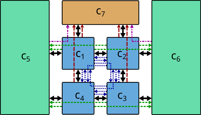
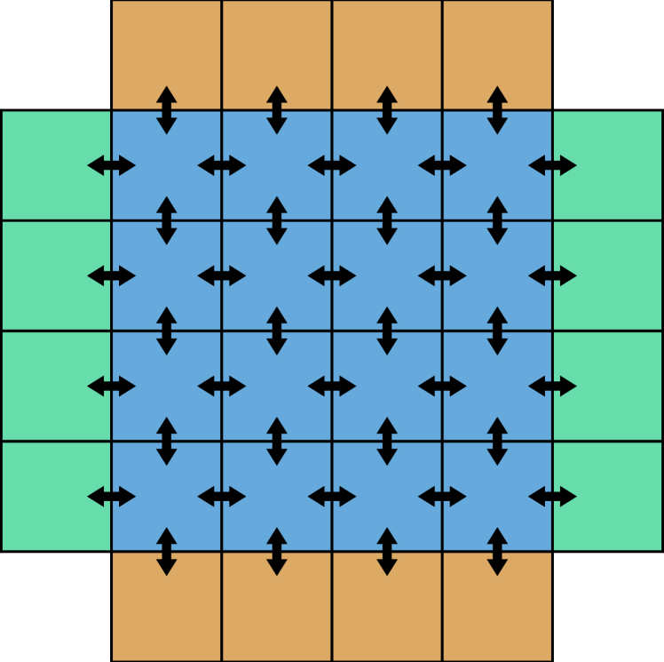
On-chip traffic can be categorized into four types: compute-to-compute (C2C), compute-to-memory (C2M), compute-to-IO (C2I), and memory-to-IO (M2I) traffic (see Fig. 1). C2C traffic originates from explicit communication between compute chiplets, or from control-messages in cache coherency protocols. C2M traffic is caused by a core accessing a shared scratchpad memory (SPM) or from coherency traffic between the L1 and L2 cache. C2I traffic is initiated by a core accessing an off-chip resource, e.g., main memory. M2I traffic originates from cache coherency traffic between the L2 cache and main memory.

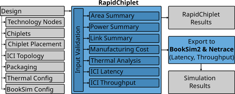
3. The RapidChiplet Architecture
We introduce RapidChiplet, a fast toolchain for rapid design-space exploration of chiplet architectures. Fig. 2 provides an overview of the RapidChiplet architecture. A design file containing links to the seven different input files is passed to RapidChiplet, which then reads and validates these input files. RapidChiplet computes seven different metrics. To minimize runtime, each metric can be toggled on and off using command line arguments. The results are stored in a results file. For more accurate ICI latency and throughput results at the cost of a higher runtime, RapidChiplet is able to run simulations using the BookSim2 (Jiang et al., 2013) network-on-chip (NoC) simulator. We extend BookSim2 with additional synthetic traffic patterns, the integration of Netrace (Hestness et al., 2010) for dependency-drive, trace-based simulations, and many more features.
3.1. Inputs Files
We explain the seven input files read by RapidChiplet. These files can be combined in arbitrary ways, i.e., we can have many designs with the same chiplets but different placements or with the same placement but different topologies.
-
•
Technology Nodes: A list of technologies, each with a PHY-latency, wafer-radius, wafer-cost, and defect density.
-
•
Chiplets: A list of chiplets, each with dimensions, a type (compute, memory, or IO), PHY locations, a technology (a key to the technology nodes file), power consumption, internal latency, component count (#cores, #memory-banks or #memory-controllers), and a flag specifying whether or not the chiplet can relay traffic.
-
•
Chiplet Placement: A list of chiplets, each with a position, rotation, and a name (a key to the chiplets file). For chips with an active interposer, this file also contains a list of interposer routers, each with a position and port-count.
-
•
ICI Topology: A list of links, each with two endpoints that can be PHYs of chiplets or ports of interposer-routers.
-
•
Packaging: The link routing (manhattan or euclidean), link latency (constant or length-dependent) and packaging yield. If a silicon interposer is used, this file additionally contains the interposer’s technology (a key to the technology nodes files). For active interposers, this file also contains the latency and power consumption of interposer-routers.
-
•
Thermal Config: The resolution, iteration-limit and termination-condition for the thermal simulation as well as heat exchanges parameters explained in Section 3.7.
-
•
BookSim Config: All parameters needed for simulations in BookSim2 (refer to BookSim (Jiang et al., 2013) for more details).
3.2. Input Validation
RapidChiplet validates all input files which includes checking for overlapping chiplets, PHYs used by more than one link, invalid keys to the chiplets or technology nodes file, links attached to non-existing PHYs or ports, and many more.
3.3. Area Summary
RapidChiplet computes the sum of all chiplet areas as well as the area of a minimal rectangle enclosing the whole placement. The difference between these two numbers acts as a metric of how area-efficient a given placement is.
3.4. Power Summary
RapidChiplet computes the power used by chiplets, by interposer-routers, as well as the total power consumption.
3.5. Link Summary
The link summary states the minimum, average and maximum length of a D2D link in the chip as well as a list containing the length of each D2D link.
3.6. Manufacturing Cost
In a first stage, we estimate the manufacturing cost of each chiplet type . To this end, we start by computing the number of chiplets that can be produced per wafer. Let be the area of a chiplet of type .
| (1) |
The first term represents the ratio between wafer area and chiplet area, including chiplets that only partially lie within the wafer. To correct for cut-off chiplets, we subtract the second term. Next, we compute the number of known-good-dies :
| (2) |
Finally, we compute the per-chiplet cost :
| (3) |
For chips with a silicon interposer, we compute the interposer cost analog to the chiplet cost, for chips without an interposer, we set . Finally, we compute the total cost:
| (4) |
3.7. Thermal Analysis
We use a fast and simple thermal model that divides the 2.5D stacked chip into a 2D grid. At each point in time, each grid-cell has a certain temperature. Time is discretized into multiple iterations. In each iteration, each grid-cell experiences the following effects, where is the ambient temperature and the parameters model the thermal conductivities of different materials:
-
•
If the cell contains a chiplet with power and area or an interposer-router with power , its temperature is increased by (chiplets) and/or (interposer-routers):
(5) -
•
The following amount of heat is transferred between any two adjacent grid-cells (from the hotter to the colder cell):
(6) -
•
For cells at the perimeter of the grid, the following amount of heat is removed (dissipated through the side of the chip):
(7) For cells at the corners, is removed twice.
-
•
All cells dissipate heat into the heat sink:
(8)
We run this simulation until the temperature change is below a threshold or the maximum number of iterations is exceeded.
3.8. ICI Latency Proxy
To compute the latency of the four traffic types C2C, C2M, C2I, and M2I, we represent the 2.5D stacked chip as a graph (see Fig. 3). In this graph, chiplets and interposer-routers are represented as nodes, while D2D links and links between interposer-routers are represented as edges. Each node and each edge has a latency-value associated with it: For chiplet-nodes the latency is set to the chiplet-specific internal latency representing the time it takes to route the message from the incoming PHY to either a component (core, memory-bank or memory-controller) to an outgoing PHY. For interposer-router nodes, the latency is set to the interposer-router latency . The latency of edges is set to the link latency which can be computed based on the link length or set to a constant value (configured through the packaging input file). For edges between a chiplet and an interposer-router, the PHY latency is added to the edge latency, and for edges between two chiplets, the PHY latency is added twice as a packet needs to traverse two PHYs.

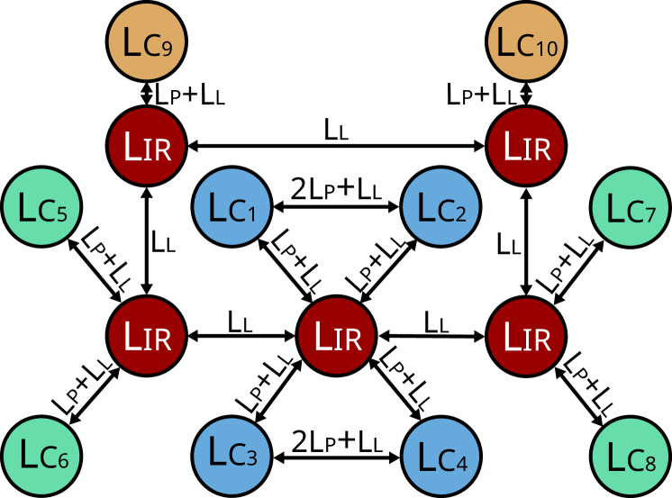
For any given traffic type, we find the shortest path between any pair of source and destination chiplets (e.g, for C2M traffic, only compute-chiplets can be the source and only memory-chiplets can be the destination). We compute the latency of each such path by finding the shortest path in the graph and summing up all node and edge latencies on the path. We report the average, minimum and maximum latency per traffic type and a list of per-path latencies.
3.9. ICI Throughput Proxy
We approximate the throughput using the same graph representation as for the latency. We use shortest path routing. The user can choose between three different routing modes for cases where multiple shortest paths exist:
-
•
default: Use the first shortest path that was found.
-
•
random: Randomly select one of the shortest paths.
-
•
balanced: Greedily balance paths across edges.
For each edge in the graph, we compute the number of paths that use that edge. The largest number of paths per edge acts as a proxy for the congestion in our network. We estimate the total communication volume per cycle as , where is the total number of paths in the given traffic type. Our throughput proxy is the injection rate, at which the sending components (compute-cores or memory banks) can inject traffic into the network. To compute it, we divide the communication volume by the number of sending components. Note that chips with more sending than receiving components have a peak injection rate below .
3.10. Export to BookSim2 (+Netrace)
BookSim2 (Jiang et al., 2013) is an established, cycle-accurate NoC simulator, however, it only supports synthetic traffic patterns. We extend BookSim2 by adding support for real traffic traces. We use Netrace (Hestness et al., 2010; Hestness and Keckler, 2011) to read the traces and identify dependencies between different packets. We implement two modes for trace-based simulations: In the Authentic mode, a packet is injected into the network once all dependencies are fulfilled and the cycle, in which the packet appears in the trace, is reached. This represents a real scenario where the compute cores need some time to read a packet, perform some computations and inject a new packet into the network. In the Idealized mode, a packet is injected as soon as all dependencies are satisfied (modelling indefinitely fast cores). We further extend BookSim2 by adding new synthetic traffic patterns for random-uniform C2C, C2M, C2I, and M2I traffic. Additionally, we modify the routing function in BookSim to only route traffic through chiplets with relay capability.
In BookSim2, one specifies the injection rate and runs the simulation to identify the average packet latency under that rate. While this is sufficient to identify the ICI’s zero-load latency, it requires multiple runs to determine the saturation throughput. We provide a wrapper for BookSim2 that runs multiple simulations with increasing injection rates to identify the saturation throughput with , , or precision. For 10% precision, we simply increase the injection load by in each step until we reach saturation. For precision, we transition from -steps to -steps when we are close to saturation and for precision, we even use -steps.
3.11. Additional Utilities
-
•
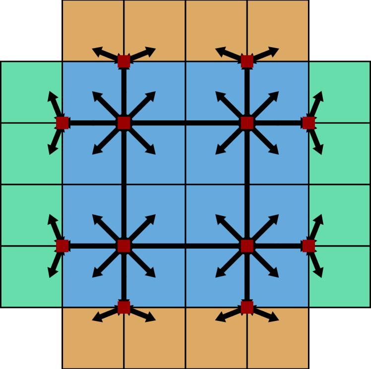
Visualizer: A tool to visualize single chiplets and whole chips. The images in Fig. 6 are created using this tool.
-
•
Generators: A set of parameterized generators for established chiplet placements and ICI topologies.
4. Evaluation
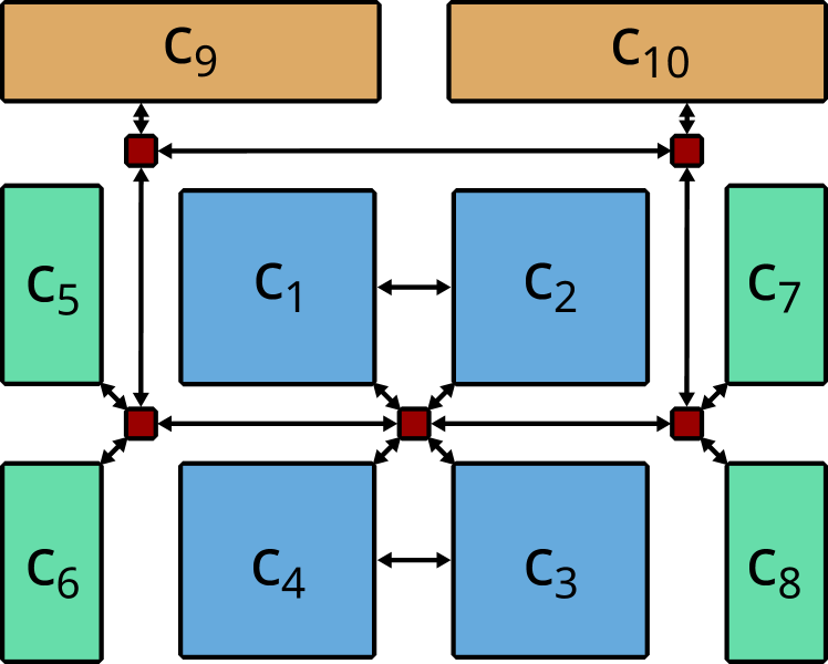
We evaluate the runtime and accuracy of RapidChiplet on a set of chips containing a 2D grid of compute-chiplets with equal-sized memory-chiplets on the left/right and IO-chiplets on the top/bottom. We vary the scale from compute chiplets up to compute chiplets, and we use two topologies, a mesh on a passive interposer and a concentrated mesh on an active interposer. Fig. 6 shows two example for the scale . We set the internal latency of chiplets and the interposer-router latency to cycles, the PHY latency to cycles, and the link latency to 1 cycle for the passive interposer, and to cycles/mm for the active interposer. All experiments are performed on a laptop with an Intel Core i7-1165G7 CPU running Arch Linux with kernel version 6.5.5.

4.1. Runtime Analysis
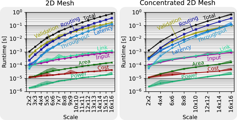
Fig. 7 breaks down the runtime of RapidChiplet into time spent for input reading, input validation, computing the area, power and link summaries, computing the manufacturing cost, constructing the routing tables and estimating the latency and throughput. We omit the runtime of the thermal analysis, since it heavily depends on the grid resolution and the termination criterion. We observe that for the smallest design, all six metrics can be computed in a single millisecond. For large designs with compute chiplets plus memory- and IO-chiplets, one second is sufficient to compute all six metrics. Note that each of the six metrics can be toggled on and off, therefore, the total runtime can significantly decrease if only a subset of the metrics is selected. Moreover, input files are only read and validated if they are needed for the selected metrics.
4.2. Comparison to BookSim2
We compare the accuracy and runtime of our latency and throughput proxies to cycle-accurate simulations in BookSim2 (Jiang et al., 2013). An important input parameter affecting both the runtime and accuracy of BookSim2 is the sample period (i.e., how many cycles do we simulate). We discovered that for small designs, BookSim2’s results stay stable after about 500 cycles, while for large designs, about 5000 cycles are required. Hence, we adjust the sample period based on the scale of a design.
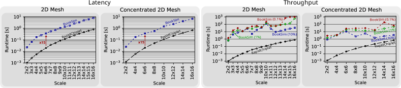
Fig. 4 compares the runtime of computing all six metrics in RapidChiplet to that of identifying the zero-load latency or saturation throughput using BookSim2. We show the runtime of BookSim2 for throughput results with , , and precision. Our process of identifying the saturation throughput by running multiply simulations with increasing loads introduces a dependency of the runtime of BookSim2 on the throughput result, which is the reason for the unstable runtime of BookSim2 in the throughput plot. Table 1 shows the average speedup of RapidChiplet over BookSim2. The reason for the higher speedup in throughput compared to latency is that computing the latency with BookSim2 only requires one simulation at low load (few packets to simulate), while computing the throughput requires multiple simulations with high loads (many packets). We conclude that RapidChiplet delivers a speedup between one and three orders of magnitude.
| Metric (precision) | Speedup 2D Mesh | Speedup Concentrated 2D Mesh |
| Latency | ||
| Throughput (10%) | ||
| Throughput (1%) | ||
| Throughput (0.1%) |
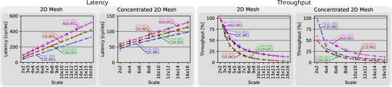
Fig. 5 compares the latency and throughput proxies of RapidChiplet to the results of BookSim2. Table 2 states the average relative error for each traffic type. Despite the high speedup of RapidChiplet over cycle-accurate simulations, its latency proxy only differs from the simulation-based result by - and its throughput proxy only differs by -. This proves that RapidChiplet is suitable for design space explorations where one needs to quickly assess countless designs and where a small accuracy loss is acceptable.
| Traffic | 2D Mesh | Concentrated 2D Mesh | ||
| Latency | Throughput | Latency | Throughput | |
| C2C | 2.69 % | 6.29 % | 4.37 % | 12.61 % |
| C2M | 1.97 % | 6.84 % | 4.36 % | 14.6 % |
| C2I | 2.82 % | 7.10 % | 4.14 % | 14.75 % |
| M2I | 3.44 % | 7.56 % | 3.27 % | 3.61 % |
5. Related Work
Various tools for early-stage design space exploration exist, however, they usually focus on a single metric or on a subset of the relevant metrics. Most of these tools are slightly more accurate but significantly slower than RapidChiplet.
ChipletActuary (Feng and Ma, 2022) is a cost model for chiplet architectures considering both the recurring engineering (RE) and non-recurring engineering (NRE) cost. Other cost models for 2.5D stacked chips, like the one by Tang et al. (Tang and Xie, 2022) have been proposed. HotSpot (Huang et al., 2006) is an established tool for thermal simulations. More recently, thermal models specifically for chiplet architectures, like, e.g., the work by Wang et al. (Wang et al., 2023) have been developed.
For early-stage latency and throughput predictions, cycle-accurate simulators such as BookSim2 (Jiang et al., 2013), Noxim (Catania et al., 2015), Nostrum (Lu et al., 2005) or Garnet (Agarwal et al., 2009) are frequently used. While these simulators were originally conceived for NoC simulations in monolithic chips, methodologies (Zhi et al., 2021) to use them for simulations of 2.5D stacked chips have been proposed. As we have shown, running cycle-accurate simulations takes orders of magnitude longer than our latency and throughput proxies. For cases where the cycle-accurate results required, RapidChiplet provides a seamless integration of BookSim2 (Jiang et al., 2013).
6. Conclusion
The design space for chiplet architectures is huge, as there are countless options for packaging, chiplet placement, D2D link implementation, ICI topology and many more. When exploring this design space, we are interested in many metrics such as chip area, power consumption, thermal properties, manufacturing cost, ICI latency, and ICI throughput. Exploring this large design space requires a fast framework capable of providing estimates for all relevant metrics.
As we are not aware of an existing toolchain satisfying these requirements, we propose RapidChiplet, a fast and unified toolchain to estimate the seven most relevant metrics of chiplet architectures. RapidChiplet only takes some microseconds to predict these metrics for designs with tens of chiplets and only a second for designs with more than 300 chiplets. Our latency and throughput proxies are up to and faster than cycle-accurate simulations while only deviating by - and - from simulation-based results.
Due to its short execution time, RapidChiplet is suitable as a cost function to both traditional optimization algorithms such as simulated annealing as well as novel, machine learning based optimization methods. By providing the open-source RapidChiplet toolchain, we facilitate exploring the complex design space of chiplet architectures, sparking future advancements in this active research area.
Acknowledgements
This work was supported by the ETH Future Computing Laboratory (EFCL), financed by a donation from Huawei Technologies.
It also received funding from the European Research Council
![]() (Project PSAP,
No. 101002047) and from the European Union’s HE research
and innovation programme under the grant agreement No. 101070141 (Project GLACIATION).
(Project PSAP,
No. 101002047) and from the European Union’s HE research
and innovation programme under the grant agreement No. 101070141 (Project GLACIATION).
References
- (1)
- uci ([n. d.]) [n. d.]. Universal Chiplet Interconnect Express (UCIe) Specification. https://www.uciexpress.org/specification.
- Agarwal et al. (2009) Niket Agarwal, Tushar Krishna, Li-Shiuan Peh, and Niraj K Jha. 2009. GARNET: A detailed on-chip network model inside a full-system simulator. In 2009 IEEE international symposium on performance analysis of systems and software. IEEE, 33–42.
- Ardalan et al. (2020) Shahab Ardalan, Halil Cirit, Ramin Farjad, Mark Kuemerle, Ken Poulton, Suresh Subramanian, and Bapiraju Vinnakota. 2020. Bunch of wires: An open die-to-die interface. In 2020 IEEE Symposium on High-Performance Interconnects (HOTI). IEEE, 9–16.
- Bharadwaj et al. (2020) Srikant Bharadwaj, Jieming Yin, Bradford Beckmann, and Tushar Krishna. 2020. Kite: A family of heterogeneous interposer topologies enabled via accurate interconnect modeling. In 2020 57th ACM/IEEE Design Automation Conference (DAC). IEEE, 1–6.
- Catania et al. (2015) Vincenzo Catania, Andrea Mineo, Salvatore Monteleone, Maurizio Palesi, and Davide Patti. 2015. Noxim: An open, extensible and cycle-accurate network on chip simulator. In 2015 IEEE 26th international conference on application-specific systems, architectures and processors (ASAP). IEEE, 162–163.
- Coskun et al. (2020) Ayse Coskun, Furkan Eris, Ajay Joshi, Andrew B Kahng, Yenai Ma, Aditya Narayan, and Vaishnav Srinivas. 2020. Cross-layer co-optimization of network design and chiplet placement in 2.5-D systems. IEEE Transactions on Computer-Aided Design of Integrated Circuits and Systems 39, 12 (2020), 5183–5196.
- Dehlaghi and Carusone (2016) Behzad Dehlaghi and Anthony Chan Carusone. 2016. A 0.3 pJ/bit 20 Gb/s/wire parallel interface for die-to-die communication. IEEE Journal of Solid-State Circuits 51, 11 (2016), 2690–2701.
- Feng and Ma (2022) Yinxiao Feng and Kaisheng Ma. 2022. Chiplet actuary: A quantitative cost model and multi-chiplet architecture exploration. In Proceedings of the 59th ACM/IEEE Design Automation Conference. 121–126.
- Graening et al. (2023) Alexander Graening, Saptadeep Pal, and Puneet Gupta. 2023. Chiplets: How Small is too Small?. In 2023 60th ACM/IEEE Design Automation Conference (DAC). IEEE, 1–6.
- Hestness et al. (2010) Joel Hestness, Boris Grot, and Stephen W Keckler. 2010. Netrace: dependency-driven trace-based network-on-chip simulation. In Proceedings of the Third International Workshop on Network on Chip Architectures. 31–36.
- Hestness and Keckler (2011) Joel Hestness and Stephen W Keckler. 2011. Netrace: Dependency-tracking traces for efficient network-on-chip experimentation. The University of Texas at Austin, Dept. of Computer Science, Tech. Rep (2011).
- Huang et al. (2006) Wei Huang, Shougata Ghosh, Sivakumar Velusamy, Karthik Sankaranarayanan, Kevin Skadron, and Mircea R Stan. 2006. HotSpot: A compact thermal modeling methodology for early-stage VLSI design. IEEE Transactions on very large scale integration (VLSI) systems 14, 5 (2006), 501–513.
- Iff et al. (2023) Patrick Iff, Maciej Besta, Matheus Cavalcante, Tim Fischer, Luca Benini, and Torsten Hoefler. 2023. HexaMesh: Scaling to hundreds of chiplets with an optimized chiplet arrangement. In 2023 60th ACM/IEEE Design Automation Conference (DAC). IEEE, 1–6.
- Jerger et al. (2014) Natalie Enright Jerger, Ajaykumar Kannan, Zimo Li, and Gabriel H Loh. 2014. NoC architectures for silicon interposer systems: Why pay for more wires when you can get them (from your interposer) for free?. In 2014 47th Annual IEEE/ACM International Symposium on Microarchitecture. IEEE, 458–470.
- Jiang et al. (2013) Nan Jiang, Daniel U Becker, George Michelogiannakis, James Balfour, Brian Towles, David E Shaw, John Kim, and William J Dally. 2013. A detailed and flexible cycle-accurate network-on-chip simulator. In 2013 IEEE international symposium on performance analysis of systems and software (ISPASS). IEEE, 86–96.
- Kannan et al. (2015) Ajaykumar Kannan, Natalie Enright Jerger, and Gabriel H Loh. 2015. Enabling interposer-based disintegration of multi-core processors. In Proceedings of the 48th international symposium on Microarchitecture. 546–558.
- Lau and Lau (2021) John H Lau and John H Lau. 2021. Chiplet Heterogeneous Integration. Semiconductor Advanced Packaging (2021), 413–439.
- Lee et al. (2020) Hyung-Jin Lee, Ravi Mahajan, Farhana Sheikh, Ramune Nagisetty, and Manish Deo. 2020. Multi-die integration using advanced packaging technologies. In 2020 IEEE Custom Integrated Circuits Conference (CICC). IEEE, 1–7.
- Li et al. (2020) Tao Li, Jie Hou, Jinli Yan, Rulin Liu, Hui Yang, and Zhigang Sun. 2020. Chiplet heterogeneous integration technology-Status and challenges. Electronics 9, 4 (2020), 670.
- Lu et al. (2005) Zhonghai Lu, Rikard Thid, Mikael Millberg, Erland Nilsson, and Axel Jantsch. 2005. NNSE: Nostrum network-on-chip simulation environment. Proc. of SSoCC (2005).
- Mahajan et al. (2016) Ravi Mahajan, Robert Sankman, Neha Patel, Dae-Woo Kim, Kemal Aygun, Zhiguo Qian, Yidnekachew Mekonnen, Islam Salama, Sujit Sharan, Deepti Iyengar, et al. 2016. Embedded multi-die interconnect bridge (EMIB)–a high density, high bandwidth packaging interconnect. In 2016 IEEE 66th Electronic Components and Technology Conference (ECTC). IEEE, 557–565.
- Moore et al. (1965) Gordon E Moore et al. 1965. Cramming more components onto integrated circuits.
- Naffziger et al. (2021) Samuel Naffziger, Noah Beck, Thomas Burd, Kevin Lepak, Gabriel H Loh, Mahesh Subramony, and Sean White. 2021. Pioneering chiplet technology and design for the amd epyc™ and ryzen™ processor families: Industrial product. In 2021 ACM/IEEE 48th Annual International Symposium on Computer Architecture (ISCA). IEEE, 57–70.
- Nishi et al. (2023) Yoshinori Nishi, John W Poulton, Walker J Turner, Xi Chen, Sanquan Song, Brian Zimmer, Stephen G Tell, Nikola Nedovic, John M Wilson, William J Dally, et al. 2023. A 0.297-pJ/Bit 50.4-Gb/s/Wire Inverter-Based Short-Reach Simultaneous Bi-Directional Transceiver for Die-to-Die Interface in 5-nm CMOS. IEEE Journal of Solid-State Circuits 58, 4 (2023), 1062–1073.
- Shabani and Guo (2019) Hesam Shabani and Xiaochen Guo. 2019. Cluscross: a new topology for silicon interposer-based Network-on-Chip. In Proceedings of the 13th IEEE/ACM International Symposium on Networks-on-Chip. 1–8.
- Sharifpour et al. (2021) Babak Sharifpour, Mohammad Sharifpour, and Midia Reshadi. 2021. SID-Mesh: Diagonal Mesh Topology for Silicon Interposer in 2.5 D NoC with Introducing a New Routing Algorithm. In 2021 ACM/IEEE International Workshop on System Level Interconnect Prediction (SLIP). IEEE, 44–51.
- Sikka et al. (2021) Kamal Sikka, Ravi Bonam, Yang Liu, Paul Andry, Dishit Parekh, Aakrati Jain, Marc Bergendahl, Rama Divakaruni, Maryse Cournoyer, Pascale Gagnon, et al. 2021. Direct bonded heterogeneous integration (DBHi) Si bridge. In 2021 IEEE 71st Electronic Components and Technology Conference (ECTC). IEEE, 136–147.
- Tang and Xie (2022) Tianqi Tang and Yuan Xie. 2022. Cost-Aware Exploration for Chiplet-Based Architecture with Advanced Packaging Technologies. arXiv preprint arXiv:2206.07308 (2022).
- Vivet et al. (2020) Pascal Vivet, Eric Guthmuller, Yvain Thonnart, Gael Pillonnet, César Fuguet, Ivan Miro-Panades, Guillaume Moritz, Jean Durupt, Christian Bernard, Didier Varreau, et al. 2020. IntAct: A 96-core processor with six chiplets 3D-stacked on an active interposer with distributed interconnects and integrated power management. IEEE Journal of Solid-State Circuits 56, 1 (2020), 79–97.
- Wang et al. (2023) Chenghan Wang, Qinzhi Xu, Chuanjun Nie, He Cao, Jianyun Liu, and Zhiqiang Li. 2023. An efficient thermal model of chiplet heterogeneous integration system for steady-state temperature prediction. Microelectronics Reliability 146 (2023), 115006.
- Zhi et al. (2021) Haocong Zhi, Xianuo Xu, Weijian Han, Zhilin Gao, Xiaohang Wang, Maurizio Palesi, Amit Kumar Singh, and Letian Huang. 2021. A methodology for simulating multi-chiplet systems using open-source simulators. In Proceedings of the Eight Annual ACM International Conference on Nanoscale Computing and Communication. 1–6.