Harnessing excitons at the nanoscale - photoelectrical platform for quantitative sensing and imaging
Abstract
Excitons — quasiparticles formed by the binding of an electron and a hole through electrostatic attraction — hold promise in the fields of quantum light confinement and optoelectronic sensing. Atomically thin transition metal dichalcogenides (TMDs) provide a versatile platform for hosting and manipulating excitons, given their robust Coulomb interactions and exceptional sensitivity to dielectric environments. In this study, we introduce a cryogenic scanning probe photoelectrical sensing platform, termed exciton-resonant microwave impedance microscopy (ER-MIM). ER-MIM enables ultra-sensitive probing of exciton polarons and their Rydberg states at the nanoscale. Utilizing this technique, we explore the interplay between excitons and material properties, including carrier density, in-plane electric field, and dielectric screening. Furthermore, we employ deep learning for automated data analysis and quantitative extraction of electrical information, unveiling the potential of exciton-assisted nano-electrometry. Our findings establish an invaluable sensing platform and readout mechanism, advancing our understanding of exciton excitations and their applications in the quantum realm.
One of the fundamental tenets of quantum mechanics is the existence of discrete energy levels, which underpins various applications in the field of quantum technology. For instance, qubits, the building blocks of quantum computing and communication, leverage this concept to perform complex calculations1. Quantum sensing techniques that make use of discrete energy levels, such as nitrogen-vacancy and Rydberg atom sensing, enable precise detection of electric and magnetic field2; 3; 4. The success of these techniques and the aspiration to probe additional physical quantities at the nanoscale motivate the development of novel discrete energy systems and sensing mechanisms.
While most of the collective excitations in quantum materials form continuous energy bands, there are certain types of discretized energy states due to quantum confinement, disruption of crystalline order or strong magnetic fields. One type of collective excitation, exciton, has discrete energy levels from the Coulomb attraction between the negatively charged electron and the positively charged hole. Their energy structure, coherence, and interactions with photons make excitons an ideal candidate for sensing devices5; 6; 7. Atomically thin transition metal dichalcogenides (TMDs) are particularly attractive for hosting robust excitonic effects, stemming from their large binding energies, direct bandgap, and pronounced light-matter interactions 8; 9. The intrinsic Coulomb interactions within excitons give rise to strong exciton-exciton and exciton-phonon coupling, culminating in intriguing phenomena such as exciton condensation and the formation of, e,g., trions10 and exciton-polarons11. Under an electric field, these interactions can substantially alter exciton properties, impacting quantities like binding energies, radiative lifetimes, and emission spectra12. The rich response of excitons to external stimuli suggests the potential for effective control and sensing. Importantly, in compact two-dimensional (2D) heterostructures, excitons provide the capability for high sensing accuracy, as they can be positioned in close proximity to the samples13; 14; 15; 16.
To successfully harness excitons as nanoscale sensors, the development of an excitation and imaging method is imperative. Detecting excitons locally is a critical first step, allowing one to gather precise data without disturbing the quantum mechanical properties. While tip-enhanced photoluminescence (TEPL) techniques have been used to study nanoscale excited state recombination in TMDs at room temperature 17; 18; 6; 19; 20, and scattering-type scanning near-field optical microscopes (s-SNOM) have provided insights into the complex dielectric function of excitons 21; 22 and their waveguide modes 23; 24; 25, these methods face limitations. Precise sensing requires a narrow exciton absorption linewidth, typically achieved at lower temperatures with direct optical excitation. However, both methods become challenging at extremely low temperatures (i.e., below 4 K), and spectroscopic measurements of excitons have only been demonstrated at room temperature so far. Additionally, emission experiments are susceptible to quenching due to environmental factors, complicating the analysis of exciton-environment interactions. These multifaceted challenges underscore the pressing need for an innovative hyperspectral imaging technique that can fully capture the fine spectroscopic details of excitons at the nanoscale in a cryogenic environment.
In this study, we develop an advanced technique, exciton resonant microwave impedance microscopy (ER-MIM), to visualize excitons with nanoscale precision at extremely low cryogenic temperatures. By combining the spectral resolution of optical spectroscopy with the high spatial resolution and enhanced sensitivity to complex dielectric response at microwave regime of MIM, we gain deep insights into exciton dynamics and their interactions with the local environment. This simultaneous imaging of dielectric responses and spectroscopic measurements of exciton energies at nano-scale enable the implementation of machine learning algorithms to reconstruct the all three important electrical quantities — conductivity, electric field and surrounding permittivity. This “all-in-one” capability for local electrical sensing paves the way for advances in quantum material-based sensing.
I Results
I.1 Local optoelectronic detection of discrete exciton Rydberg states
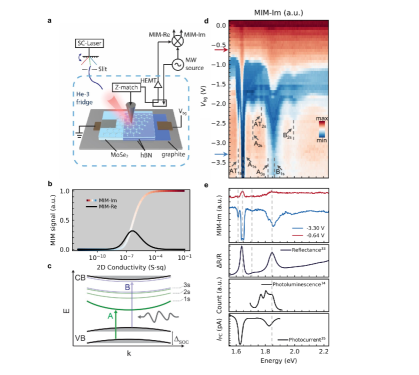
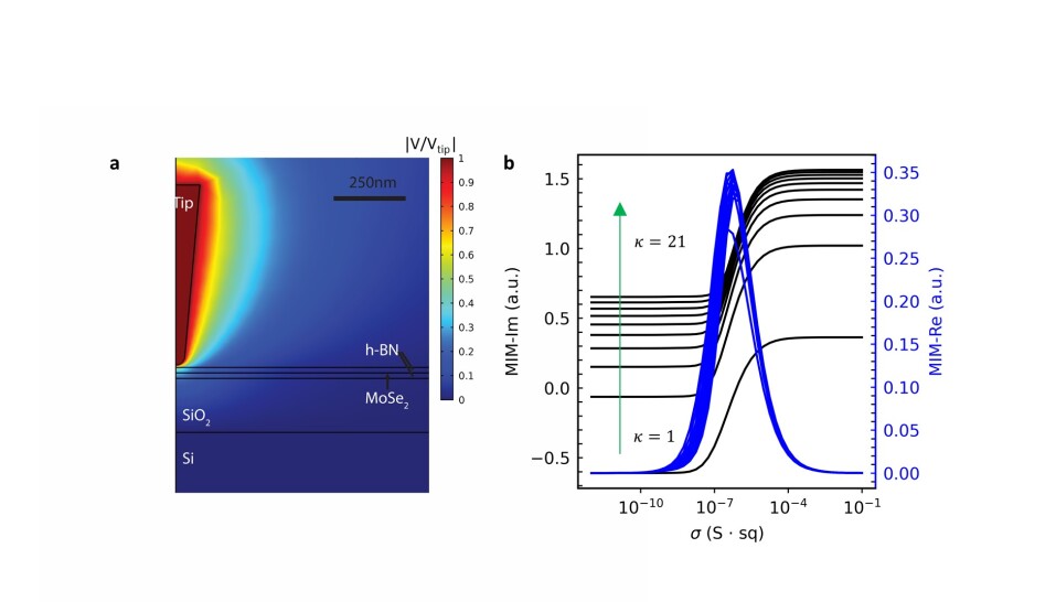
We first introduce the ER-MIM technique that enables us to sense excitons using photoelectrical effects at the nanoscale. As shown in Fig. 1a, our setup consists of two parts: a microwave transmission line impedance-matched to a metallic scanning probe (tip) 26; 27; 28, and a continuously wavelength-tunable laser that is fiber-coupled into a Helium-3 cryostat and illuminates the tip. The real and imaginary parts of the reflected microwave signals are recorded, which are in- and out-of-phase with the reference microwave excitation line, respectively. Our measurements were conducted at 1.5 K and 3 GHz, yet this method can readily be adapted to even lower temperatures (e.g., the base temperature of the Helium-3 cryostat). In Fig. 1b, we present two calculated response curves that illustrate the relationship between the real (in-phase) and imaginary (out-of-phase) parts of the reflected microwave signals and the local complex conductivity of the sample.
The material we study is a prototypical 2D TMD device — a monolayer of MoSe2 encapsulated within hBN layers with graphite as a back gate. The optical spectrum of monolayer MoSe2 possesses a series of pronounced resonances, categorized as A- and B-excitons (see Fig. 1c). These excitons arise from two optical transitions involving states in the upper and lower energy spin valence bands. They possess Rydberg atom-like energy levels, each designated by its principal quantum number, .
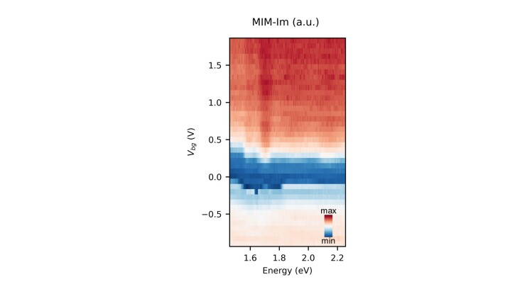
We track the evolution of the microwave response as a function of excitation wavelength and back gate voltage controlling the free carrier density in MoSe2 (imaginary part of the ER-MIM signal shown in Fig. 1d). From the response curve in Fig. 1b, the blue and red colored regions correspond to low and high conductivity of MoSe2, respectively. The overall dependence of conductivity on back gate voltage agrees with the transfer curve of a semiconductor, i.e., it decreases when crossing from the conduction band into the bandgap, and increases when entering the valence band. On top of this overall trend, at specific photon energies (e.g., 1.65 eV), the conductivity has an extra increase at smaller (e.g., 2V), and another decrease at large (e.g., 2V). We identify those photon energies as in resonance with neutral and excitons, and the excited Rydberg states including , , and , as well as weaker modulations in intensity features corresponding to their charged counterparts like and (which are usually referred to as trion or exciton polaron, and their distinction will be discussed below).
The changes in ER-MIM-Im signal near excitonic resonances imply the observation of photoconductivity associated with exciton formation. The sign flip from positive (red) at small to negative (blue) at large can be attributed to two major processes (a discussion on ruling out other possible optical processes in note 2 29). One is the photoconductive effect 26, where the exposure of TMD-based devices to light generates neutral electron-hole pairs. Then, the trapping of one carrier and the release of the other free carrier from an exciton could result in an enhanced conductivity 30. This process explains our observation of positive conductivity near excitonic resonances. The other is the Auger assisted tunneling effect31; 32. When the photon energy is in resonance with the binding energy of excitons, a generated exciton can excite a free hole when it recombines during the Auger process. The hole can subsequently tunnel through the hBN barrier to reach the bottom gate, which effectively reduces the MoSe2 conductivity. Since the energy barrier on the hole side between MoSe2 and hBN is much smaller than the electron side, the negative photoconductivity is only observed when MoSe2 is hole-doped 29. Therefore, the conductivity decrease at large is attributed to the dominance of the Auger effect.
We further compare two linecuts of ER-MIM-Im spectrum with previously reported far-field spectra of excitons in monolayer MoSe2 (Fig. 1e). The red and blue curves show excitonic peaks and dips, highlighting the signal from the photoconductivity and Auger-assisted tunneling effects, respectively. The comparison reveals excellent agreement between the identified exciton energies in ER-MIM-Im and the results obtained from optical reflectance33, photoluminescence34, and photocurrent35 measurements. It is noteworthy that our spectral resolution stands on par with, or surpasses, those of the above-mentioned area-averaged methods. This compelling correspondence demonstrates that our ER-MIM technique enables accurate photoelectric measurements of exciton spectra with the added benefit of exceptional spatial resolution and access to a temperature regime that has, until now, been unattainable.
I.2 The interplay between excitons and the charge environment
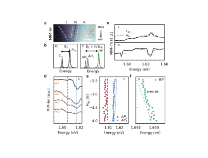
To untangle the exciton-electron interactions at the nanoscale, we modulate carrier density of MoSe2 by controlling applied onto graphite while collecting ER-MIM spectra (Fig. 1a). The graphite boundary splits MoSe2 into three distinct spatial regions (Fig. 2a): (I) a region that extends beyond the graphite back gate (BG) that is ungated, (II) the region directly above the BG, in which the carrier density is controlled by , and (III) the depletion region associated with the nanojunction between regions I and II. Our focus lies on contrasting the ER-MIM responses in regions I and II, which are distant from the junction and hence less influenced by the electric field, yet differentiated by their carrier densities. Such a comparative approach enables a systematic exploration of excitonic behaviors in diverse local charge environments.
Fig. 2b depicts two scenarios of exciton-electron interactions. The first involves trions, charged and weakly coupled three-particle complexes formed by binding two electrons (or holes) to one hole (or electron). Trion and exciton eigenenergies differ by the trion binding energy, denoted as (left schematic). The second scenario features charge-neutral bosons resulting from excitons interacting with the degenerate Fermi sea of excess charge carriers (right schematic). In this context, excitons become dressed by Fermi sea excitations, giving rise to attractive and repulsive exciton-polaron (AP and RP) quasiparticles, akin to Fermi-polarons in the context of cold atoms 34; 11. The energy difference between AP and RP branches, or the exciton polaron binding energy is approximately , with representing the Fermi energy 11. To examine these two physical pictures, we take advantage of the sensitivity of ER-MIM spectra to (gate)-tunable local excitonic energy levels.
In the upper panel of Fig. 2c, we present the ER-MIM spectrum obtained in region I. This region is not strongly affected by the back gate voltage, hence close to intrinsically (-)doped. The spectrum reveals one major resonance feature at 1.642 eV, corresponding to exciton (fitting shown as a grey dashed line). Notably, at 1.5 K, the linewidth of the exciton dip is 2.5 meV, closely approaching the theoretically calculated intrinsic linewidth of excitons 36. Similar linewidth was observed in the spectrum measured in the more -doped region III (shown in the lower panel of Fig. 2c). The spectrum shows one more prominent feature centered at 1.59 eV, corresponding to trion (fitting shown as a grey dotted line).
On the other hand, we conducted spatially-resolved ER-MIM measurements at four distinct locations spaced 50 nm apart in -doped region II (Fig. 2a, spots 1-4) at a constant . The line spectra zoomed in near the trion resonance energy are shown in Fig. 2d. This region has the highest carrier density among the three, and the formerly designated in region III feature divides into two separated dips (marked by the red dashed and blue dotted lines). Moreover, the intensity of the two dips exhibits significant variations across different spots.
To further understand the spatial dependence, we measured the back gate dependence of the ER-MIM spectra sitting at spot 4. The red and blue circles in Fig. 2e are extracted exciton eigenenergies at different near formerly designated , and the green circles in Fig. 2f are another eigenenergy near formerly designated . The red dashed and blue dotted branches display nearly linear redshifts while the exciton energy demonstrates a linear blueshift with . This trend remains consistent throughout the range of in our experiments. The increasing energy separation between the branches in Fig. 2e and the other one in Fig. 2f is a signature of exciton-polaron formation at elevated carrier doping levels (Fig. 2b). In this framework, the formerly assigned becomes repulsive exciton-polaron (RP). The branch turns into attractive exciton-polarons (AP1 and AP2), where the splitting between AP1 and AP2, a feature obscured in far field experiments but restored in ER-MIM signal, can be understood as excitons coupling with the Fermi seas in two different valleys (Fig. 2b).
The observed gate-dependent shifts in AP and RP eigenenergies indicate interactions between excitons and free carriers. These energy shifts exhibit an almost linear dependence on , reflecting a collective effect of carrier density dependent exciton binding energy change, quasiparticle bandgap renormalization, and the variation of binding energy of the exciton polaron. To quantify the shifts, we introduce a coefficient , where , with being the change of eigenenergy of an exciton polaron state which has a linear dependence on carrier density . The observed nanoscale spatial variation of suggests that the eigenenergy changes can be used as a sensitive local indicator of the charge environment.
I.3 The interplay between excitons and the electric environment
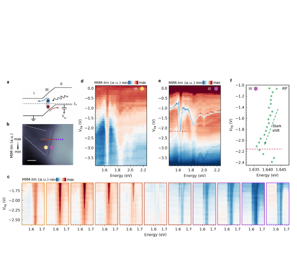
In addition to the charge environment, to understand the intricate interplay between excitons and the local electrical variations, we examine more closely the ER-MIM signals in region III, the depletion area. Here, an in-plane electric field propels electrons and holes towards regions I and II, respectively. We also compare the the excitonic response closeby and farther away from the controlled - junction, i.e., region III and region II, as illustrated in the schematic in Fig. 3a.
To start with, a systematic ER-MIM scan across the - junction was carried out as a function of and excitation energy. We mark the locations in Fig. 3b and plot the results in Fig. 3c. It is evident that a continuous variation in the ER-MIM-Im signal near the AP and RP resonances is observed across the - junction. Especially, when on resonance, there is a continuous change from positive to negative photoconductivity from the left-hand side of the nanojunction to the right-hand side. This marks the conversion from a photoconductive effect-dominated mechanism in the ungated region of MoSe2 to Auger tunneling-dominated mechanism in the back-gated region of MoSe2.
The field effect is then studied in greater detail via high-resolution imaging in region III (Fig. 3d and 3e, with locations marked by stars in Fig. 3b). The two gate-dependent spectra in region III both appear to be very different from the ones obtained from region II (Fig. 1b). They feature mostly positive photoconductivity at excitonic resonances (red colored regions), and less change with gating. Within region III, measurement in the right part (purple star in Fig. 3b, Fig. 3e) shows a relatively more effective gating effect, where the restoration of some negative photoconductivity can be identified. This observation further elucidates the - junction behavior in region III.
To study the excitonic response to electric field, we extracted the RP eigenenergy from Fig. 3e, and plot it in Fig. 3f. There are two distinct features that differ from region II (Fig. 2f): the RP energy exhibits an overall redshift behavior with doping level, instead of a blueshift; the RP energy has an abrupt blueshift at V. The first feature agrees with the dc Stark effect of excitons: , where is the exciton polarizability 12, represents the electric field strength and signifies the energy shift. The second feature underscores the nonlocal effect of the dielectric constant on exciton energies. Since a carrier density gradient exists in this region, when the right part of the sample goes across the band edge, it leads to a sharp increase in carrier compressibility (n being carrier density, and being the chemical potential), which then changes the exciton screening in the left part. This is consistent with the Coulomb potential screening of excitons through a free electron gas, which leads to another describable dependency of excitons on the environmental permittivity: . These observations suggest how excitons can serve as imaging tools for a - junction and reveal intricate nanoscale parameters such as electric field and dielectric constant.
I.4 Quantitative photoelectrical imaging and exciton-facilitated electrometry
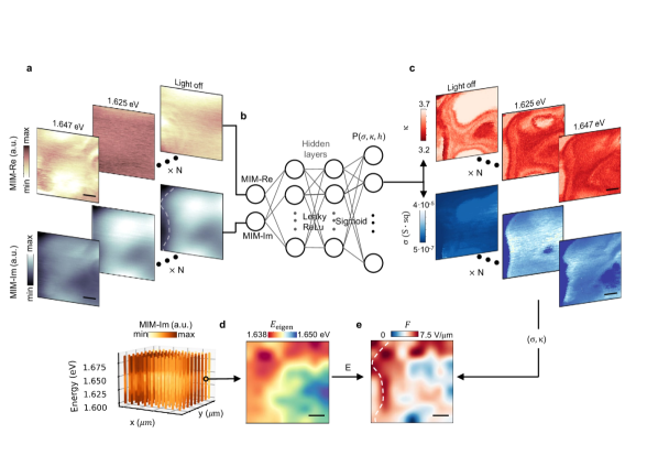
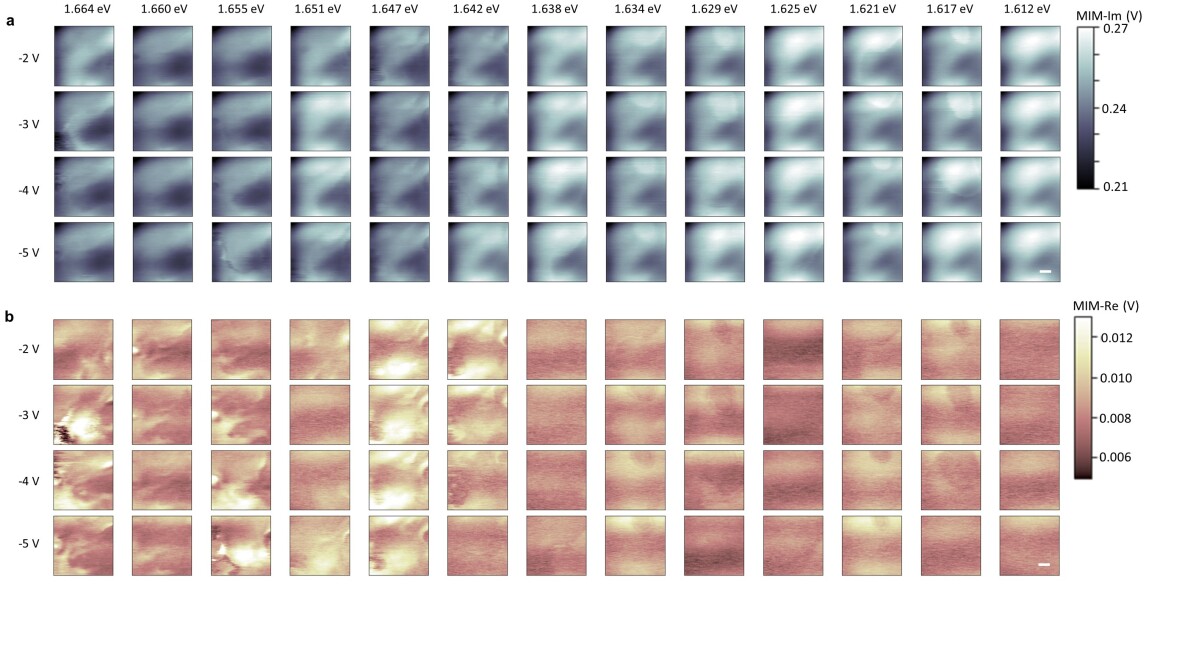
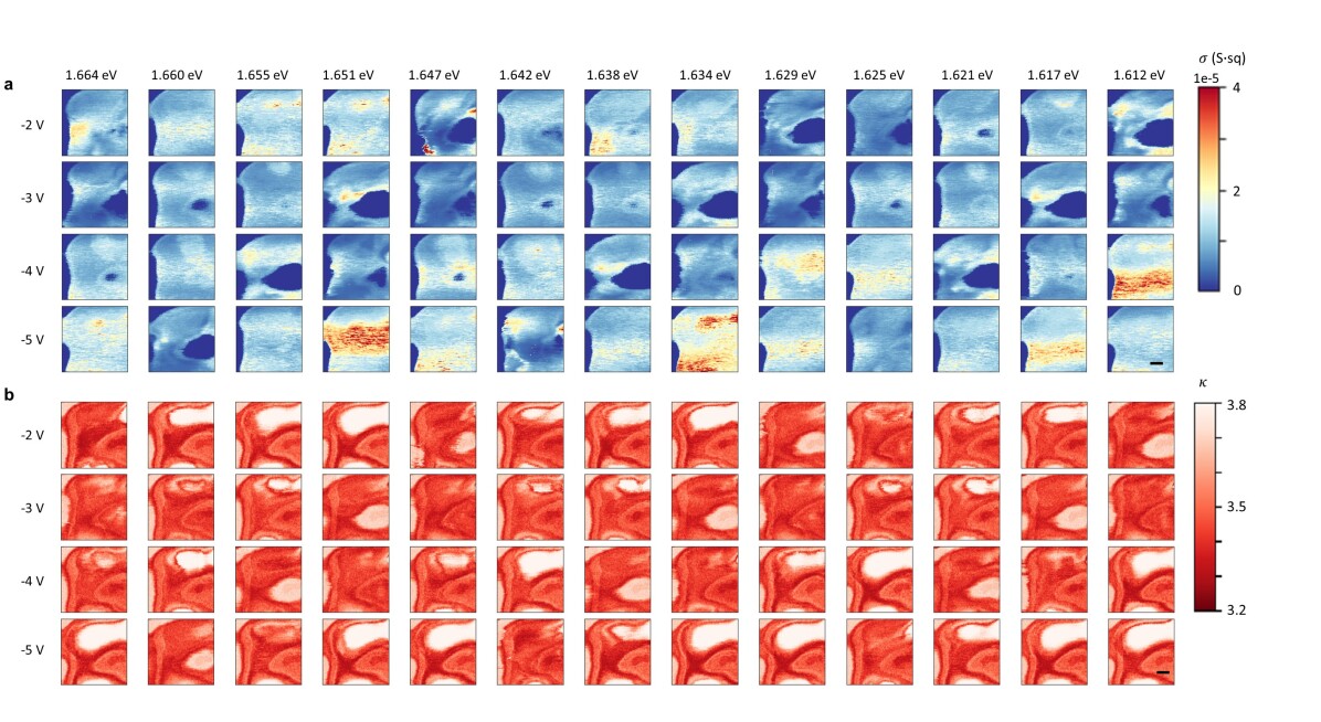
To quantitatively analyze the ER-MIM data and utilize it for predicting material properties, we developed a deep neural network (DNN) 37; 38; 39; 40; 41 based on a set of MIM maps. These maps consist of 256100 pixel images, obtained with variations in optical excitation energies and back gate voltages within a 1 m 1 m region at the graphite back gate boundary. Due to the complex, multidimensional nature of the datasets, traditional fitting approaches prove to be inadequate. In Fig. 4a, we present three representative sets of MIM-Im and MIM-Re data collected at , under different conditions: with the light off, under 1.651 eV light excitation, and 1.655 eV light excitation (complete dataset in 29). The 1.651 eV excitation is off-resonance with excitons, while the 1.655 eV excitation is close to the resonance of RP branch of the exciton.
In the following, we show how to use this DNN to predict the local environment, (, , ), i.e., sheet conductivity of MoSe2, the relative permittivity of the hBN-MoSe2-hBN stack, and relative tip-sample distance , for a given MIM data set. We construct a feedforward network (Fig. 4b), with the inputs being MIM-Re and MIM-Im, either from the experiment or finite element simulations42; 29, and predict the probability at each set of discretized values. We train the network with a total of 64,000 sets of simulation data, which is divided into bins along the , , and directions. Each data point is encoded into a 3840-dimensional vector with the elements being its bin membership – 1 for a member and 0 for a non-member. Given the absence of a direct correlation between MIM-Re and MIM-Im, and , we adopt a Binary Cross Entropy loss function. In this way, we transform the prediction into a classification problem, where the network output represents the probability for each bin. A good agreement is found between the deep neural network outputs and the ground truth 29.
We then apply the trained network to predict the probability distribution of for a given set of MIM maps in Fig. 4a. The results of are shown in Fig. 4c. The obtained maps indicate the presence of local dielectric disorder in the environmental permittivity, as well as permittivity change of MoSe2 upon back gate doping and optical excitation. The obtained maps present the spatially dispersive photoconductivity from the RP exciton polaron. These quantified maps hence provide a direct measure of the local environment of excitons.
Following the quantification of maps and our understanding of the exciton eigenenergies variation due to charge and electrical environment, as discussed in the last two sections, we formulate the subsequent expression to describe the local exciton eigenenergy 29:
| (1) |
The first term of the expression, , represents the exciton eigenenergy for monolayer MoSe2 under the influence of environmental permittivity, without further considering exciton-electron interactions or electric field effects. The second term represents the interaction between the exciton and free carriers. The variable corresponds to carrier density, and is a fitting coefficient. The linear relationship is extracted from experimental results, such as Fig. 2f, and the coefficient is derived from the back gate sweeping data. Since this term results from a combination of both bandgap renormalization and the reduction in exciton binding energies with carrier doping, and these effects largely cancel each other out, it is not a main contribution to spatial eigenenergy fluctuation. The third term accounts for the Stark effect resulting from in-plane electric fields with strength . The contribution from out-of-plane electric field is negligible since the in-plane exciton polarizability is approximately two orders of magnitude larger than the out-of-plane value due to hBN dielectric screening 43. In our measurements, the Stark shift term dominates the spatial variation of exciton eigenenergy .
Subsequently, we determine the exciton eigenenergies on the 2D grid within the same 1 m 1 m region, through fitting and interpolating the MIM hyperspectra. The extracted is presented in Fig. 4d. With and the corresponding DNN-predicted as inputs for solving Eqn. (1), we generate the predicted electric field distribution, which is illustrated in Fig. 4e. It is evident that the exciton-assisted prediction of the electric field map effectively captures the hotspots in the nanojunction at the graphite boundary (marked as white dotted line), which agrees well in width and amplitude with the finite element simulation results29 (Fig. S7). Moreover, it captures the built-in field in other regions hundreds of nanometers away from the junction (i.e., in region II). This result reveals that the photoelectrical properties of a prototypical 2D TMD device are influenced by a combination of factors, such as the Schottky field and fluctuations in conductivity manifested as localized charge puddles. It highlights the critical role of the electric field, which is dispersive on the sub-diffraction limit scale and emphasizes the need to consider the complex interaction of various electrical properties for accurate assessment in 2D materials-based optoelectronic applications. Moreover, this result demonstrates the effectiveness of exciton-assisted electrometry, and the “all in one” readout of multiple electrical quantities, which is general and can be applied for nano-electrical sensing in a wide variety of quantum systems, demonstrating its potential and versatility in quantum applications.
II Conclusions
Our work represents a significant advance in the field of nano-imaging for exciton dynamics. The ER-MIM introduces an attempt to drive optoelectronics into the nanoscale, with distinct advantages over traditional methods including superior sensitivity with a low requirement for excitation photon flux, applicability under extreme cryogenic conditions, and high spatial and spectral resolutions. The application of ER-MIM to a gate tunable monolayer MoSe2 device uncovered the intricate interplay between excitons, charge carriers, and built-in electrical fields in a confined dielectric environment at cryogenic temperatures. Employing a neural network, we developed an algorithm for quantitatively determining the local electric field, conductivity, and environmental permittivity. These insights lay the foundations for employing exciton as an all-in-one sensor for local electrical information and mark a leap in advancing sensing modalities for quantum materials and devices.
III Methods
The full sample fabrication procedure is detailed in ref.44. Briefly, graphene, hBN, and MoSe2 were exfoliated from bulk crystals onto Si/SiO2 (285 nm) substrates and assembled in heterostructures using a standard dry-transfer technique with a poly(bisphenol A carbonate) film on a polydimethylsiloxane (PDMS) stamp. MoSe2 was encapsulated between two approximately 30 nm thick hBN flakes. Electron beam lithography and electron beam metal deposition were used to fabricate electrodes for the electrical contacts.
The exciton resonant microwave impedance microscopy (ER-MIM) experiment was conducted with a supercontinuum laser (NKT photonics, FIU-20). The wavelength scans were carried out with a monochromator (Princeton instrument, Acton SP 2300). The linewidth after the monochromator is around 0.5 nm. The laser power at the end of the 100 m diameter multimode fiber is 0.1–1 mW throughout the measurements, with the spot radius at the end of the tip being around 0.8 mm.
IV Acknowledgements
Funding: This work was supported by the QSQM, an Energy Frontier Research Center funded by the U.S. Department of Energy (DOE), Office of Science, Basic Energy Sciences (BES), under Award #DE-SC0021238. Previous development of MIM technique was funded in part by the Gordon and Betty Moore Foundation’s EPiQS Initiative through Grant GBMF4546 to ZXS. B. E. F. acknowledges support from NSF-DMR-2103910 for sample fabrication. K.W. and T.T. acknowledge support from the JSPS KAKENHI (Grant Numbers 20H00354 and 23H02052) and World Premier International Research Center Initiative (WPI), MEXT, Japan. Part of this work was performed at the Stanford Nano Shared Facilities (SNSF), supported by the National Science Foundation under award ECCS-2026822. Z. J. and Z. Z. acknowledge support from the Stanford Science fellowship. Z.J. acknowledge support from the Urbanek-Chodorow fellowship. M.K.L. acknowledges support from the NSF Faculty Early Career Development Program under Grant No. DMR - 2045425. The research is funded in part by a QuantEmX grant from ICAM and the Gordon and Betty Moore Foundation through Grant GBMF9616 to M.K.L. M.K.L. also acknowledges helpful discussion with Xinzhong Chen. Z.Z. acknowledges helpful discussions with Houssam Yassin. Z.J. acknowledges helpful discussions with Tony Heinz and Dung-Hai Lee.
References
- (1) Saffman, M., Walker, T. G. & Mølmer, K. Quantum information with rydberg atoms. Reviews of modern physics 82, 2313 (2010).
- (2) Casola, F., Van Der Sar, T. & Yacoby, A. Probing condensed matter physics with magnetometry based on nitrogen-vacancy centres in diamond. Nature Reviews Materials 3, 1–13 (2018).
- (3) Schirhagl, R., Chang, K., Loretz, M. & Degen, C. L. Nitrogen-vacancy centers in diamond: nanoscale sensors for physics and biology. Annual review of physical chemistry 65, 83–105 (2014).
- (4) Degen, C. L., Reinhard, F. & Cappellaro, P. Quantum sensing. Reviews of modern physics 89, 035002 (2017).
- (5) Popert, A. et al. Optical sensing of fractional quantum hall effect in graphene. Nano Letters 22, 7363–7369 (2022).
- (6) Chand, S. B. et al. Visualization of dark excitons in semiconductor monolayers for high-sensitivity strain sensing. Nano Letters 22, 3087–3094 (2022).
- (7) Xu, Y. et al. Correlated insulating states at fractional fillings of moiré superlattices. Nature 587, 214–218 (2020).
- (8) Manzeli, S., Ovchinnikov, D., Pasquier, D., Yazyev, O. V. & Kis, A. 2d transition metal dichalcogenides. Nature Reviews Materials 2, 1–15 (2017).
- (9) Wang, G. et al. Colloquium: Excitons in atomically thin transition metal dichalcogenides. Reviews of Modern Physics 90, 021001 (2018).
- (10) Lui, C. et al. Trion-induced negative photoconductivity in monolayer mos 2. Physical review letters 113, 166801 (2014).
- (11) Efimkin, D. K., Laird, E. K., Levinsen, J., Parish, M. M. & MacDonald, A. H. Electron-exciton interactions in the exciton-polaron problem. Physical Review B 103, 075417 (2021).
- (12) Klein, J. et al. Stark effect spectroscopy of mono-and few-layer mos2. Nano letters 16, 1554–1559 (2016).
- (13) Mak, K. F. & Shan, J. Semiconductor moiré materials. Nature Nanotechnology 17, 686–695 (2022).
- (14) Regan, E. C. et al. Emerging exciton physics in transition metal dichalcogenide heterobilayers. Nature Reviews Materials 7, 778–795 (2022).
- (15) Cai, J. et al. Signatures of fractional quantum anomalous hall states in twisted mote2. Nature 622, 63–68 (2023).
- (16) Regan, E. C. et al. Mott and generalized wigner crystal states in wse2/ws2 moiré superlattices. Nature 579, 359–363 (2020).
- (17) Bao, W. et al. Visualizing nanoscale excitonic relaxation properties of disordered edges and grain boundaries in monolayer molybdenum disulfide. Nature communications 6, 7993 (2015).
- (18) Darlington, T. P. et al. Imaging strain-localized excitons in nanoscale bubbles of monolayer wse2 at room temperature. Nature Nanotechnology 15, 854–860 (2020).
- (19) Zhou, J. et al. Near-field coupling with a nanoimprinted probe for dark exciton nanoimaging in monolayer wse2. Nano letters (2023).
- (20) Hasz, K., Hu, Z., Park, K.-D. & Raschke, M. B. Tip-enhanced dark exciton nanoimaging and local strain control in monolayer wse2. Nano Letters 23, 198–204 (2022).
- (21) Plankl, M. et al. Subcycle contact-free nanoscopy of ultrafast interlayer transport in atomically thin heterostructures. Nature Photonics 15, 594–600 (2021).
- (22) Zhang, S. et al. Nano-spectroscopy of excitons in atomically thin transition metal dichalcogenides. Nature communications 13, 542 (2022).
- (23) Hu, F. et al. Imaging exciton–polariton transport in mose2 waveguides. Nature Photonics 11, 356–360 (2017).
- (24) Luan, Y. et al. Imaging anisotropic waveguide exciton polaritons in tin sulfide. Nano Letters 22, 1497–1503 (2022).
- (25) Iyer, R. B., Luan, Y., Shinar, R., Shinar, J. & Fei, Z. Nano-optical imaging of exciton–plasmon polaritons in wse 2/au heterostructures. Nanoscale 14, 15663–15668 (2022).
- (26) Chu, Z. et al. Unveiling defect-mediated carrier dynamics in monolayer semiconductors by spatiotemporal microwave imaging. Proceedings of the National Academy of Sciences 117, 13908–13913 (2020).
- (27) Barber, M. E., Ma, E. Y. & Shen, Z.-X. Microwave impedance microscopy and its application to quantum materials. Nature Reviews Physics 4, 61–74 (2022).
- (28) Cui, Y.-T., Ma, E. Y. & Shen, Z.-X. Quartz tuning fork based microwave impedance microscopy. Review of Scientific Instruments 87 (2016).
- (29) Supplementary Materials, which includes reference .
- (30) Handa, T. et al. Spontaneous exciton dissociation in transition metal dichalcogenide monolayers. arXiv preprint arXiv:2306.10814 (2023).
- (31) Chow, C. M. E. et al. Monolayer semiconductor auger detector. Nano Letters 20, 5538–5543 (2020).
- (32) Sushko, A. et al. Asymmetric photoelectric effect: Auger-assisted hot hole photocurrents in transition metal dichalcogenides. Nanophotonics 10, 105–113 (2020).
- (33) Arora, A., Nogajewski, K., Molas, M., Koperski, M. & Potemski, M. Exciton band structure in layered mose 2: from a monolayer to the bulk limit. Nanoscale 7, 20769–20775 (2015).
- (34) Liu, E. et al. Exciton-polaron rydberg states in monolayer mose2 and wse2. Nature communications 12, 6131 (2021).
- (35) Vaquero, D., Salvador-Sánchez, J., Clericò, V., Diez, E. & Quereda, J. The low-temperature photocurrent spectrum of monolayer mose2: Excitonic features and gate voltage dependence. Nanomaterials 12, 322 (2022).
- (36) Selig, M. et al. Excitonic linewidth and coherence lifetime in monolayer transition metal dichalcogenides. Nature communications 7, 13279 (2016).
- (37) Kalinin, S. V., Sumpter, B. G. & Archibald, R. K. Big–deep–smart data in imaging for guiding materials design. Nature materials 14, 973–980 (2015).
- (38) Krull, A., Hirsch, P., Rother, C., Schiffrin, A. & Krull, C. Artificial-intelligence-driven scanning probe microscopy. Communications Physics 3, 54 (2020).
- (39) Kalinin, S. V. et al. Automated and autonomous experiments in electron and scanning probe microscopy. ACS nano 15, 12604–12627 (2021).
- (40) Chen, X. et al. Machine learning for optical scanning probe nanoscopy. Advanced Materials 35, 2109171 (2023).
- (41) Kelley, K. P. et al. Fast scanning probe microscopy via machine learning: non-rectangular scans with compressed sensing and gaussian process optimization. Small 16, 2002878 (2020).
- (42) Multiphysics, C. Introduction to comsol multiphysics®. COMSOL Multiphysics, Burlington, MA, accessed Feb 9, 2018 (1998).
- (43) Pedersen, T. G. Exciton stark shift and electroabsorption in monolayer transition-metal dichalcogenides. Physical Review B 94, 125424 (2016).
- (44) Kometter, C. R. et al. Hofstadter states and re-entrant charge order in a semiconductor moiré lattice. Nature Physics 1–7 (2023).
- (45) Laturia, A., Van de Put, M. L. & Vandenberghe, W. G. Dielectric properties of hexagonal boron nitride and transition metal dichalcogenides: from monolayer to bulk. npj 2D Materials and Applications 2, 6 (2018).
- (46) Raja, A. et al. Dielectric disorder in two-dimensional materials. Nature nanotechnology 14, 832–837 (2019).
- (47) Shan, J.-Y., Pierce, A. & Ma, E. Y. Universal signal scaling in microwave impedance microscopy. Applied Physics Letters 121 (2022).
- (48) Massicotte, M. et al. Dissociation of two-dimensional excitons in monolayer wse2. Nature communications 9, 1633 (2018).
- (49) Ju, L. et al. Photoinduced doping in heterostructures of graphene and boron nitride. Nature nanotechnology 9, 348–352 (2014).
- (50) Thureja, D. et al. Electrically tunable quantum confinement of neutral excitons. Nature 606, 298–304 (2022).
- (51) Kormányos, A. et al. k· p theory for two-dimensional transition metal dichalcogenide semiconductors. 2D Materials 2, 022001 (2015).
- (52) Xiao, K., Kan, C. & Cui, X. Coulomb potential screening via charged carriers and charge-neutral dipoles/excitons in two-dimensional case. arXiv preprint arXiv:2309.14101 (2023).
- (53) Lu, Y. et al. Giant built-in electric field enabled quantum-confined stark effects (2023).
- (54) Biswas, S. et al. Rydberg excitons and trions in monolayer mote2. ACS nano 17, 7685–7694 (2023).
- (55) Heckötter, J. et al. Scaling laws of rydberg excitons. Physical Review B 96, 125142 (2017).
Supplementary information for “Harnessing excitons at the nanoscale - photoelectrical platform for quantitative sensing and imaging”
I Finite-element analysis of the MIM signals
Finite-element analysis (FEA) of the MIM response to 2D sheet conductance is shown in Fig. S1. For the tip-sample geometry in Fig. S1a, the tip radius is chosen to be 50 nm, and the distance above the sample surface 10 nm. The sample parameters are: The monolayer MoSe2 is 1 nm in thickness, both top and bottom hBN layers are 30 nm in thickness. The hBN - MoSe2 - hBN slab is approximated with a uniform relative permittivity , since hBN and MoSe2 have similar quasi-static dielectric constants 45; 46. The SiO2 substrate is 300 nm thick with = 3.9. The simulated MIM-Im, MIM-Re response curves as a function of the sheet conductance of and relative permittivity of the slab are shown in Fig. S1b. Both simulations with and without the graphite layer were conducted, and they differ by a scaling factor, so the simulation result is shown in arbitrary units.
II Possible origins of the ER-MIM response
To understand the origins of the ER-MIM response, we discuss different photoconductivity generation mechanisms in a 2D TMD device upon exciton formation and dissociation.
1. Microwave induced dissociation of exctions: With an input power of 0.2 W, and considering the gain offered by the half-wave impedance-match section, the GHz voltage at the tip is on the order of 0.01 V 47. Then, with the tip radius parameter of 50 nm, and considering the dielectric constant of hBN, we estimate that the typical electric field at the sample is less than 0.1 V/m. This is much smaller than the gate voltage applied to the monolayer and hence not considered a major process 48.
2. Photogating effect: The photogating effect can be excited through direct photoactivation of midgap charged defects in hBN 49. But the observation that the photoconductivity has dips near the exciton absorption resonances implies that it depends on the exciton population in MoSe2, instead of the hBN defect population itself, which rules out this mechanism. For the other type of photogating effect proposed to be happening at interfaces, our sandwiched device geometry would have two interfaces, making the segregation of electrons or holes on one specific interface relatively unlikely.
3. Auger effect: This effect is largely dependent on the band alignment of the TMD monolayer and hBN. To prove this argument, we also conduced measurements on the monolayer WSe2 part of the device (Fig. S2), where it shows less prominent ER-MIM-Im decrease at excitonic resonances with similar measurement conditions as in Fig. 1d. This is in accordance with the DFT calculation which shows a larger valence band misalignment between WSe2 and hBN and hence less tunneling 32.
4. Photoconductivity: The exposure of TMD-based devices to light can generate photo-carriers resulting in an enhanced conductivity. The dissociation of electron hole pairs is fostered by the existence of defects, including hole traps in the MoSe2. A similar enhancement of photoconductivity near excitonic excitations were measured on monolayer WSe2 (Fig. S2, vertical stripes in dark red color).
III Details of the machine learning algorithm
Our goal is to predict the local environment (, , ) for a given set of MIM real and imaginary measurements, MIM-Re and MIM-Im. However, this mapping is not bijective, as multiple sets of (, , ) can correspond to the same (MIM-Re, MIM-Im). Therefore, instead of predicting a fixed (, , ), we assign a probability to each set of (, , ) for a given measurement. Figure 4 in the main text shows the feedforward network architecture used for predicting local properties. The network takes input values of MIM-Re and MIM-Im, either from experiments or simulations and predicts the probability distribution for discretized values.
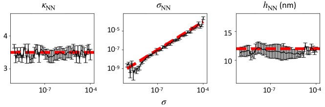
For training the network, we start by simulating MIM-Re and MIM-Im for various sets of . We then interpolate this simulation data across a physically relevant range of values: from to Ssq, between 3.2 and 3.9 45, and from 6 to 18 nm, with even spacing in each dimension. This amounts to a total of 64,000 sets of data. We further divide the data into bins: 32 bins for , 8 bins for , and 15 bins for , resulting in 3,840 bins in total. Each data point is then encoded into a 3,840-dimensional one-hot encoding vector based on its bin membership. During training, we minimize the Binary Cross Entropy loss, transforming the prediction into a classification problem, where the network output is a 3,840-dimensional vector representing the probabilities for each bin.
The network architecture consists of 2 hidden layers with 100 nodes each. We use the Adam optimizer with a constant learning rate of and set and to 0.999 and 0.9999, respectively. We train until the variance of the loss function over the last 200 steps falls below . Data is randomly split into 80% for training, 10% for validation, and 10% for testing. Figure S3 shows the neural network predictions for interpolated simulation data with varying conductivity and random noise amplitude 4%. The predictions and the ground truth agree within errorbars for all values of conductivity.
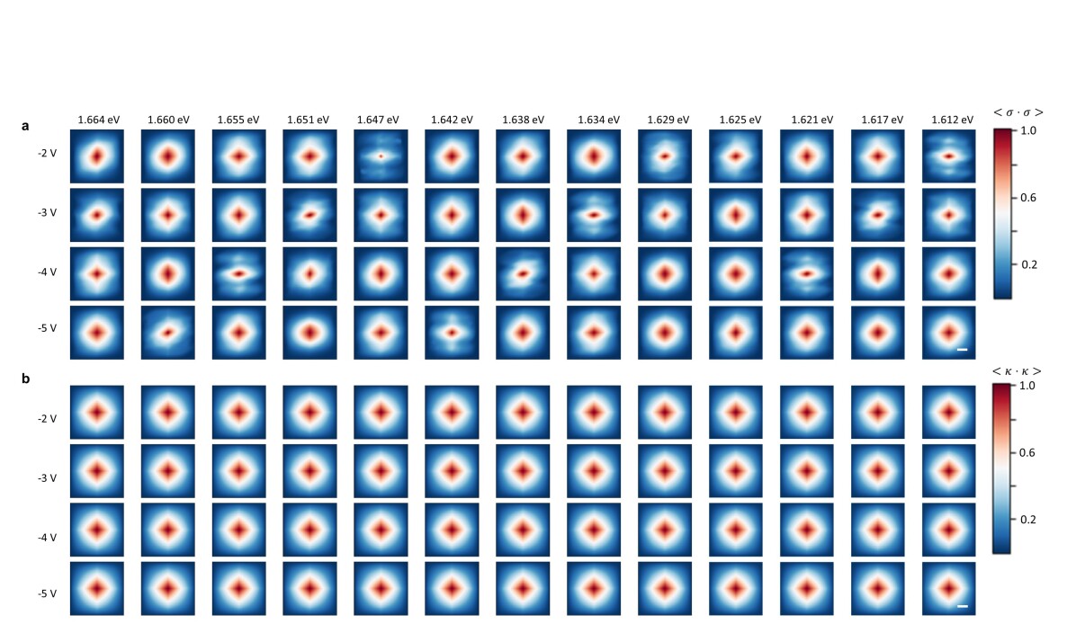
We proceed to apply the trained network to predict the probability distribution of for a given set of MIM maps in Fig. S4. All the measurements are of the same region of the sample so the sample topography is the same for all the different data sets. To fix the height distribution, we first condition one set of MIM measurements to be similar to an initial guess distribution, consisting of a jump in height with a smooth edge at the junction as well as a two-dimensional Gaussian distribution on the right representing a bubble. To achieve this, we calculate the distance, , of each bin from as and weight the predicted probability distribution with , where denotes the constraint strength (with in this case). In addition, we impose a smoothness condition by encouraging the neighboring pixels to be similar. For all predictions, we average over 20 samples per pixel. The results of are shown in the first two columns of Fig. S5. The prediction for and share some similarities, due to the presence of local fluctuations in environmental permittivity, or dielectric disorder, as well as charge screening effects. Furthermore, when comparing among different sets of , the contrast is observed between excitation energy close or further away from the excitonic resonances. These quantified maps hence provide a direct measure of the exciton-induced photoconductivity and the impact of the dielectric environment.
Figure S6 shows the autocorrelated images of and . Notably, while the correlation of relative permittivity remains relativity consistent, the normalized autocorrelation of conductivity has a decrease when the RP branch of excitons is on resonance. This decrease is more prominent along the vertical direction, perpendicular to the direction of the - junction. It provides a signature of exciton excitation induced conductivity variation, and supports the self-consistency of the approach.
IV Details of electric field prediction
IV.1 Benchmarking using Comsol simulations
To cross check the electric field sensing result, we performed finite element simulations to predict the electric field distribution near the junction. In this simulation, we assumed zero temperature, and modelled the MoSe2 monolayer as a charge sheet with density 50,
| (S1) | ||||
where and are the electron and hole charge densities, respectively. They are determined by the 2D density of states ( is the effective mass). and are the conduction and valence band edge energies, respectively, which are dependent of the local electrostatic potential. is the Fermi level determined by the alignment of the contact work function with respect to the band edges.
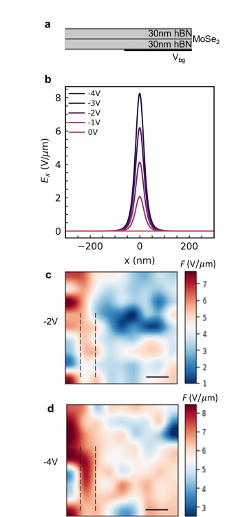
The simulated device geometry is depicted in Fig. S7. The sheet of charge is encapsulated by two 30 nm thick hBN slabs and contacted by an ohmic electrode. Furthermore, we include a gate with only partial coverage. The voltage on the back gate is 4 V in our simulations. The material parameters used for this calculation are as follows: MoSe2 band gap eV, Fermi level offset relative to the valence band edge at zero potential eV, electron effective mass , hole effective mass 51, hBN dielectric constant .
In this way, we obtain the in-plane electric field distribution depicted in Fig. S7b at various back gate voltages on the right half of the device. We then compare the electric field prediction results shown in Fig. S7 c,d, which are measured at and , respectively, with the simulation result. It shows agreement of both amplitude and width of the depletion region near the boundary.
The input of exciton eigenenergies is critical to obtain the correct electric field distribution, as direct finite element simulations from and has limitations. The limitations involve several aspects: 1) The built-in field formed by conductivity fluctuations is hard to capture without accurate measurement of carrier mobilities. 2) The sophistication of semiconductor properties of 2D TMD materials at cryogenic temperatures, including defect levels and partial ionizations is hard to quantify. 3) The optical excitation and associated quasi-equilibrium carrier dynamics are hard to quantify.
IV.2 Details of excitonic electrometry and outlook
The coefficient is derived from fitting the gate-dependent excitonic resonance energy, and the value of at is adopted. The spatial variation of is considered in calculations. The exciton polarizability is a function of the effective exciton Bohr radius () and effective exciton temperature, in a simplified formula of 52. At our measurement temperature of 1.5 K, there has not been a consensus on the value of polarizability. Our fitted value from experiment, approximately (varying with local permittivity), is larger than the theoretically calculated value of 43, while in better agreement with some recent measurements 53. This is due to the low measurement temperature, where the dependence gives rise to much larger polarizability, and also the influence from the dielectric environment. The dependence of on dielectric constant is adopted from the theoretically calculated functional form 43 and experimental fitting. The exciton binding energy change with dielectric screening is also incorporated in the form of 43.
When assuming the spectral linewidth of 0.05 meV, with these numbers, the exciton sensor has the smallest detectable field of sub 1 . The distance between an exciton sensor and a sample can be brought to very closer, due to the 2D nature of TMD monolayers. This sensitivity can be further improved by: 1) Using excitons in other TMD materials, for example in monolayer MoTe2, with almost invariant eigenenergies under changing carrier densities. It can reduce the influence of other terms in main text Eqn. (1) 54. 2) Utilizing excited Rydberg states of excitons under higher fluence photon excitation, which will yield larger polarizability (). The enhancement has been predicted to follow a scaling law, where increases with the principal quantum number () as .55 3) Utilizing exciton states with distinct in-plane and out-of-plane polarizabilities, such as interlayer excitons in a heterobilayer device. This will assist in achieving a vector electric field readout.