Nonvolatile spin field effect transistor based on VSi2N4/Sc2CO2 multiferroic heterostructure
Abstract
We report first-principles calculations that propose a nonvolatile spin field effect transistor (spin-FET) based on a van der Waals multiferroic heterostructure, i.e., VSi2N4/Sc2CO2. We find that the inversion of ferroelectric polarization of monolayer Sc2CO2 can efficiently modulate the electronic states of monolayer VSi2N4. A half-metal to half-semiconductor phase translation of VSi2N4 can be efficiently realized, which leads to distinct electronic transport properties. We additionally construct a spin-FET device based on the multiferroic heterostructure. We find that the VSi2N4/Sc2CO2 based Spin-FET has remarkable all-electric-controlled performance. A large on-off current ratio of about 650% induced by the inversion of Sc2CO2 ferroelectric polarization can be obtained under a small bias voltage (0.02 V). We also find an interesting spatially-separated spin-polarized transport phenomenon, with the pure spin-up (spin-down) electrons transporting merely in VSi2N4 (Sc2CO2). Our study provides a promising approach for constructing low-energy-dissipation and nonvolatile FET devices.
I Introduction
During the continuous miniaturization of electronic products, Joule heating and quantum limit on device becomes the bottlenecks that prevent further increase operation speed and information density, which invalidate the Moore’s law Liu ; Xie . Spintronics is believed to be the strong candidate of the future technology in the post Si-era Treger ; Marun . For any operation in spintronics, the techniques for injection, detection, manipulation, transport, and storage of spins need to be established Nitta . In spin-based devices, encoding and reading out spin information in single spins can be considered the ultimate limit for scaling magnetic information. Spin field-effect transistor (spin-FET) is a fundamental spin-based device for the spin operation Datta ; Datta1 . Developing low-power cost spin-FET that can efficiently realize the on or off state of single spin current is crucial for the development of spintronics Dieny .
Traditionally, spin-FET is a three terminal device with spin polarized current flowing between drain and source terminals and the gate terminal is used to control this current. As proposed by Datta and Das, the spin precession motion of electron can be controlled through the Rashba spin-orbit coupling effect, where on and off states are distinguished by phase difference in spin precession motion Datta ; Datta1 . Nonetheless, since the realization of phase difference in the spin-FETs depends on the precise control of gate voltage, such spin-FET device meets challenge of the nonvolatile functionality, which is usually realized by using a ferroelectric material as gating.
In this work, based on the first-principles calculations, we propose a spin-FET possessing remarkable nonvolatile on and off functionality. Such spin-FET uses a two-dimensional (2D) van der Waals (vdW) multiferroic heterostructure (e.g. composed by monolayer VSi2N4 and monolayer Sc2CO2) as the channel material, instead of the nonmagnetic semiconductors (like InAs, InAlAs, etc.) that are generally adopted in traditional spin-FET devices Parveen . In the multiferroic heterostructure, ferromagnetic material VSi2N4 has a half-semiconductor characteristic and is mainly responsible for the spin transport Lake ; Li . Whereas, the ferroelectric material Sc2CO2 has a semiconductor characteristic Yang ; Ang and is mainly in charge of controlling the spin-polarized electronic structure of VSi2N4. It is found that the inversion of ferroelectric polarization of Sc2CO2 can efficiently change the spin-up electronic structure of VSi2N4, leading to a half-semiconductor to half-metal transition. It is also found that the VSi2N4/Sc2CO2 based Spin-FET has remarkable all-electric-controlled performance, where a large on-off current ratio can be obtained under a small bias voltage. Additionally, an interesting spatially-separated spin-polarized transport phenomenon, with the pure spin-up (spin-down) electrons transporting merely in VSi2N4 (Sc2CO2), is observed.
II method
Geometric optimization and electronic structures of the heterostructure are calculated by density-functional theory (DFT) with the projector-augmented-wave (PAW) method, which is implemented in the Vienna ab initio simulation package Vasp1 ; Vasp2 . The exchange-correlation interaction is treated by the generalized gradient approximation (GGA) based on the Perdew-Burke-Ernzerhof (PBE) function and HSE06 functional for the geometric optimization and electronic structures, respectively Guo1 ; Guo2 . The convergence standards of the atomic energy and positions are less than 1 10-5 eV per atom and 1 10-2 eV Å-1, respectively. The cutoff energy of wave function is set to 500 eV. The Brillouin zone (BZ) is sampled by a 9 9 1 Monkhorst-Pack k-point mesh.
The transport properties are simulated based on the DFT method combined with the nonequilibrium Green’s function (NEGF) formalism, using the Atomistix ToolKit (ATK) 2019 package ATK . In the calculations, the Tier 3 basis set of the linear combination of atomic orbital (LCAO) is adopted with Hartwigsen-Goedecker-Hutter pseudopotentials and GGA in the form of the PBE function is utilized to represent the exchange and correlation interactions. The transmission calculations are carried out with the PBE pseudopotentials distributed in the QuantumWise package ATK ; ATK1 . A density mesh-cutoff of 75 Hartree is employed, and the BZ is sampled using a k-point grid in the transport calculations. At a bias-voltage Vb, the spin-resolved current () can be calculated as follows:
| (1) |
where and are the Fermi-Dirac distribution of the left and right electrodes, respectively. and are the electrochemical potentials of the left and right electrodes, respectively, and is the transmission probability for an electron at energy E with spin . Note that the linear response current originated from the equilibrium transmission spectrum at zero bias is considered in the calculations Guo3 .
III Results
The heterostructure is constructed by a ferromagnetic (FM) monolayer VSi2N4 and a ferroelectric monolayer Sc2CO2. The monolayer Sc2CO2 was predicted to have a sizable out-of-plane electrical polarization as high as 1.60 C/cm3, and the reverse of electric polarization is achieved via displacement of C atoms with an energy barrier about 0.52 eV Yang . The Sc2CO2 with carbon-up and carbon-down configurations correspond to the polarization-up (P) and polarization-down states (P), respectively (see Fig. 1(a)). On the other hand, VSi2N4 is a theoretically predicted 2D magnetic material, which is a member of the MA2Z4 family. The Curie temperature of monolayer VSi2N4 is predicted to be higher than room temperature, showing the promising potential applications in future spintronic devices Lake . Fig. 1(b) further shows the calculated band structure of monolayer VSi2N4. An interesting characteristic is that there is only spin-up electrons in a wide energy range around the Fermi energy (EF), i.e., [-1.7, 1.4] eV, making VSi2N4 an ideal half-semiconductor.
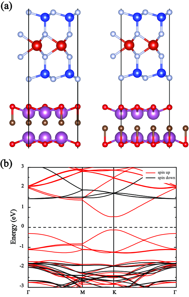
Considering that the in-plane lattice constant of freestanding Sc2CO2 and VSi2N4 are 5.74 Å and 2.88 Å, respectively, a 2 2 super-periodicity of VSi2N4 is commensurate to the 1 1 Sc2CO2, with a lattice mismatch is of 1.23%. As shown in Fig. S1, we have considered three typical stacking configurations of the VSi2N4/Sc2CO2 heterostructure, namely, hollow configuration, bridge configuration, and top configuration. The calculated total energies of the three configurations are -300.77698 eV, -300.77690, and -300.77688 eV, respectively, showing that the hollow configuration (also see Fig. 1(a)) is the most stable. Nevertheless, the total energy difference among the three configurations is very small ( 0.1 meV). This feature indicates that all the three configurations can be obtained in experiments. Moreover, it is found that the interlayer spacing between VSi2N4 and Sc2CO2 is 3.06 Å and 2.82 Å for the P and P polarization states, respectively. It is known that the atomic radii of O and N atoms, which are located at the surface of Sc2CO2 and VSi2N4, respectively, are 0.66 Å and 0.71 Å. Hence, the sum of their atomic radii is much smaller than the interlayer spacing, showing the nature of vdW interaction between Sc2CO2 and VSi2N4. To ensure that the VSi2N4/Sc2CO2 heterostructure is energetically stable, we further calculate the binding energy () between VSi2N4 and Sc2CO2, which is defined as . Here , , and are the total energy of monolayer Sc2CO2, monolayer VSi2N4, and the VSi2N4/Sc2CO2 heterostructure, respectively. represents the number of O atoms located at the interface of the heterostructure. In the hollow configuration, it is found that = -31 meV/Å2 and -21 meV/Å2 for the P and P polarization states, respectively. This result shows that the heterostructure is energetically stable under a vdW interlayer interaction.
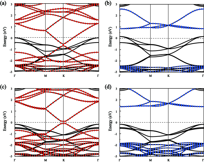
Then, we discuss the electronic properties of VSi2N4 manipulated by the polarization of Sc2CO2. In compression with the band structure of freestanding VSi2N4 (Fig. 1(b)), there is an obvious upshift of EF of VSi2N4 in the heterostructure in the P polarization state (Figs. 2(a) and 2(b)). As a result, an half-semiconductor to half-metal transition occurs in VSi2N4 under the effect of Sc2CO2. Moreover, the band gap of spin-up electrons remarkably decreases from 0.7 eV to 0.1 eV, showing the strong interface effect on the electronic structure of VSi2N4. It is noticed that the spin-up energy bands in the heterostructure present a type-III band alignment, whereas the spin-down energy bands have a type-II band alignment. This feature indicates that there is an obvious electron transfer from Sc2CO2 to VSi2N4, which fills up the spin-up conduction states. As for the case of P polarization state, the spin-up energy bands of VSi2N4 present a type-I band alignment, and the spin-down energy bands form a type-II band alignment (Figs. 2(c) and 2(d)). This result shows that there is little charge transfer between Sc2CO2 and VSi2N4. In comparison with that of freestanding VSi2N4, there is also a sizable decrease of band gap of the spin-up electrons (from 0.7 eV to 0.2 eV), whereas the band gap of spin-down electrons changes little. This result is similar to that of the P polarization state. It is noticed that the EF lies in the band gap of spin-up electrons, which makes the heterostructure a half-semiconductor. The above results show that the inversion of out-of-plane polarization of the Sc2CO2 can dramatically change the band alignment as well as the band structure of VSi2N4 in the heterostructure.
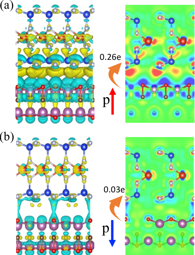
To further show the Sc2CO2 polarization dependent charge transfer effect on band structure of VSi2N4, we calculate the electron density difference (EDF) of VSi2N4/Sc2CO2 heterostructure. As shown in Fig. 3(a), there are extra electron (hole) in the VSi2N4 (Sc2CO2) part of the P configuration, compared with that of the freestanding VSi2N4 (Sc2CO2). According to Bader’s charge analysis, around 0.26 electron transfers from Sc2CO2 to VSi2N4, which results in the half-semiconductor to half-metal transition of VSi2N4. On the other hand, we do not observe any significant charge transfer from Sc2CO2 to VSi2N4 in the P configuration (see Fig. 3(b)). Hence, VSi2N4 holds the half-semiconductor characteristic. This result agrees well with the Sc2CO2-polarization dependent band alignments in the heterostructure.
In addition, the band projection analysis (Fig. S2) shows that both the conduction band minimum (CBM) and valence band maximum (VBM) of spin-up electronic states of VSi2N4 are attributed to the d and d (eg orbitals of V atoms), which locate in the center of VSi2N4. Note that the eg orbitals of V atoms also give rise to the CBM of spin-down electrons as shown in Fig. S2, and thus induce the type-II band alignment. This result shows that the atomic layer composed of V atoms is mainly responsible to the spin current transport in the VSi2N4/Sc2CO2 heterostructure.
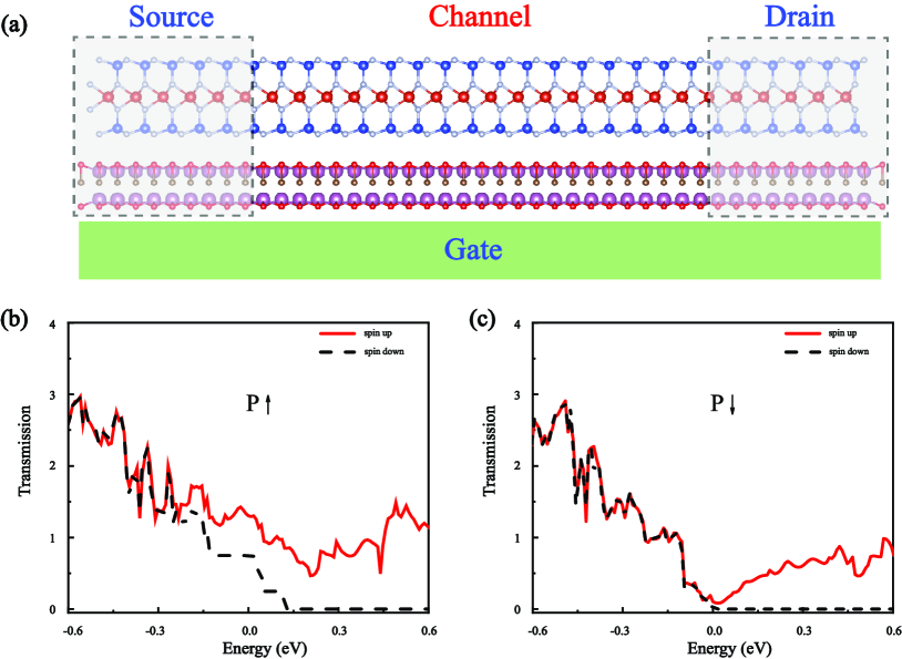
Next, we discuss the plentiful nonvolatile spin transport properties of VSi2N4 induced by the Sc2CO2 polarizations. We first propose a novel spin-FET structure based on the VSi2N4/Sc2CO2 heterostructure, as shown in Fig. 3(a). In this structure, one can effectively control the inversion of Sc2CO2 ferroelectric polarization by a bottom gate. When Sc2CO2 is in P polarization, according to the band structure of VSi2N4/Sc2CO2 shown in Fig. 2(a), one expects a large spin-up current and thus the spin-FET is in an on state, due to the half-metal characteristic of VSi2N4. In contrast, when Sc2CO2 is in P polarization, a small spin-up current and thus the off state is expected within a low bias voltage region, owing to the half-semiconductor characteristic of VSi2N4 (Figs. 2(c)). Note that, there is no spin-down current from VSi2N4, due to the large band gap of the spin-down electrons of VSi2N4 (Figs. 2(b) and 2(d)). Consequently, a pure spin-polarized current can be realized in the VSi2N4/Sc2CO2 based nonvolatile spin-FET.
To verify above argument, we further calculate the electronic transport property of the spin-FET. Figs. 4(b) and 4(c) show the transmission spectrum of this device at zero bias with Sc2CO2 in P and P polarizations, respectively. It is seen that the transmission of spin-up electrons in P condition reaches up to 1.4 at Fermi level, where as it is only 0.1 in the P polarization state. The nonzero transmission at Fermi level in the P polarization state can be attributed to the room temperature adopted in this study, which induces the broadening of band structure. As a result, an on-off ratio of 14 for the spin-up electrons of VSi2N4 can be obtained in the law bias voltage region. Notably, in the P polarization state, there is also sizable transmission at Fermi level (0.7) for the spin-down electrons, which comes entirely from Sc2CO2 (as shown in Fig. 2(b), the VBM of spin-down electrons of Sc2CO2 upshifts to 0.2 eV above EF). This result shows an interesting spatially-separated spin-polarized transport phenomenon in the spin-FET, which is expected to have potential applications in the future spintronics. Note that the transmission of spin-down electrons of both VSi2N4 and Sc2CO2 in the spin-FET goes to zero at higher energy levels, i.e., E0.15 eV and 0.01 eV with Sc2CO2 in P and P polarizations, respectively. In this condition, the spin-down current from Sc2CO2 can be completely inhibited, and thus the pure spin-up current transport can be realized. This result implies the good spin-valve performance of the VSi2N4/Sc2CO2 based devices.
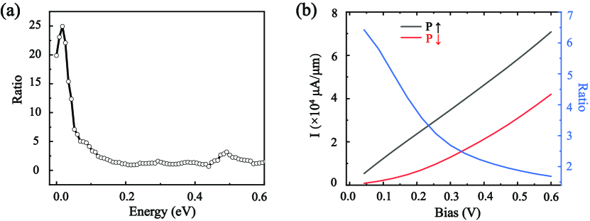
Finally, we discuss the on-off ratio of the total current in the spin-FET. Fig. 5(a) shows the on-off ratio of the total transmission (sum of spin-up and spin-down transmissions). It is seen that the on-off ratio monotonically increases with decreasing the bias voltage from 0.6 V, reaching 2500% around the Fermi level. This result indicates that a drastic total current (sum of spin-up and spin-down currents) difference can be induced by the inversion of ferroelectric polarizations of Sc2CO2 in the low bias voltage region. Fig. 5(b) further shows the calculated I-V curves of the total current in P and P polarization states, respectively. In the P state, the total current linearly increases with the bias voltage. Whereas, in the P state it quadratically increases with the bias voltage. As a result, the on-off ratio of total current monotonically increases with decreasing the voltage, and a large on-off ratio of about 650% can be obtained when a small bias voltage (0.02 V) is applied (Fig. 5(b)).
IV summary
In summary, based on the VSi2N4/Sc2CO2 multiferroic heterostructure, we propose a way of realizing nonvolatile spin-FET, which has a low-energy-consumption characteristic. The DFT calculations show that the inversion of Sc2CO2 ferroelectric polarization can efficiently modulate the spin-polarized electronic structure of VSi2N4, which induces a half metal to half-semiconductor transition. Such electronic phase transition can lead to significant change of electronic transport properties, which is an essential concept of the nonvolatile spin-FET. We additionally construct a spin-FET structure based on the VSi2N4/Sc2CO2 heterostructure. The electronic transport calculations show that the Spin-FET has remarkable all-electric-controlled performance, where a large on-off ratio (about 650%) of the total current has been obtained when a small bias voltage (0.02 V) is applied. Moreover, an interesting spatially-separated spin-polarized transport phenomenon has been observed when Sc2CO2 is in P polarization, where the pure spin-up (spin-down) electrons transport in VSi2N4 (Sc2CO2). These findings can be helpful to the design of high-performance nonvolatile 2D Spin-FET devices.
Acknowledgements.
We acknowledge financial support from the Ministry of Science and Technology of the People’s Republic of China (Grant No. 2022YFA1402901), the Natural Science Foundation of Shaanxi Province (Grant No. 2023-JC-QN-0768), and the Natural Science Foundation of China (Grant No. 12074301).References
- (1) Z. Shen, S.Jing, Y. Heng, Y. Yao, K. N. Tu, and Y. Liu, Appl. Phys. Rev. 10, 021309 (2023).
- (2) H. Li, H. Jiang, Q. F. Sun, and X. C. Xie, arXiv:2303.07692.
- (3) S. A. Wolf, A. Y. Chtchelkanova, and D. M. Treger, IBM J. Res. Dev. 50, 101 (2006).
- (4) A. Avsar, H. Ochoa, F. Guinea, B. zyilmaz, B. J. van Wees, and I. J. Vera-Marun, Rev. Mod. Phys. 92, 021003 (2020).
- (5) S. Sugahara and J. Nitta, Spin-transistor electronics: An overview and outlook, Proc. IEEE 98, 2124 (2010).
- (6) S. Datta and B. Das, Electronic analog of the electrooptic modulator, Appl. Phys. Lett. 56, 665 (1990).
- (7) B. Behin-Aein, D. Datta, S. Salahuddin, and S. Datta, Nat. Nanotechnol. 5, 266 (2010).
- (8) B. Dieny, I. L. Prejbeanu, K. Garello, P. Gambardella, P. Freitas, R. Lehndorff, W. Raberg, U. Ebels, S. O. Demokritov, and J. Akerman et al., Nature Electronics 3, 446 (2020).
- (9) G. F. A. Malik, M. A. Kharadi, F. A. Khanday, and N. Parveen, Microelectron. J. 106, 104924 (2020).
- (10) M. Rakibul Karim Akanda and R. K. Lake, Appl. Phys. Lett. 119, 052402 (2021).
- (11) L. Liang, Y. Yang, X. Wang, and X. Li, Nano Lett. 23, 858 (2023).
- (12) Y. Lu, R. Fei, X. Lu, L. Zhu, L. Wang, and L. Yang, ACS Appl. Mater. Interfaces 12, 6243 (2020).
- (13) L. Cao, X. Deng, G. Zhou, S. Liang, C. V. Nguyen, L. K. Ang, and Y. S. Ang, Phys. Rev. B 105, 165302 (2022).
- (14) G. Kresse and J. Furthmller, Phys. Rev. B 54, 11169 (1996).
- (15) G. Kresse and J. Hafner, Phys. Rev. B 47, 558 (1993).
- (16) K. Wang, Y. Zhang, W. Zhao, P. Li, J. W. Ding, G. F. Xie, and Z. X. Guo, Phys. Chem. Chem. Phys. 21, 9310 (2019).
- (17) Z. X. Guo, Y. Y. Zhang, H. J. Xiang, X. G. Gong, and A. Oshiyama, Phys. Rev. B 92, 201413(R) (2015).
- (18) S. Smidstrup, T. Markussen, P. Vancraeyveld, J. Wellendorff, J. Schneider, T. Gunst, B. Verstichel, D. Stradi, P. A. Khomyakov, U. G. Vej-Hansen et al., J. Phys.: Condens. Matter 32, 015901 (2020).
- (19) J. Huang, P. Li, X. Ren, and Z. X. Guo, Phys. Rev. Appl. 16, 044022 (2021).
- (20) B. Liu, X. X. Ren, X. Zhang, P. Li, Y. Dong, Z. X. Guo, Appl. Phys. Lett. 122, 152408 (2023).