Ultra-compact and efficient integrated multichannel mode multiplexer in silicon for few-mode fibers
Space-division multiplexing (SDM) is one of the key enabling technologies to increase the capacity of fiber communication systems. However, implementing SDM-based systems using multimode fiber has been challenging with the need for compact, low-cost, and scalable mode de/multiplexer (DE/MUX). Here we present a novel integrated mode MUX for few-mode fibers (FMFs) which can launch up to eight spatial and polarization channels. The new design is composed of a two-dimensional multimode grating coupler (MMGC), highly compact mode size converters (MSCs), and adiabatic directional couplers (ADCs). Eight data lanes in FMFs can be selectively launched with integrated optical phase shifters. Experimental results reveal efficient chip-to-fiber coupling with peak efficiencies of -3.8 dB, -5.5 dB, -3.6 dB, and -4.1 dB for LP01, LP11a, LP11b, and LP21b modes, respectively. Meanwhile, the proposed design can efficiently couple all the degenerate LP modes in a two-mode FMF, allowing signal descrambling in the demultiplexer. Thanks to the use of integrated subwavelength Mikaelian lens for mode-independent field size conversion with loss , the total footprint of the MMGC and MSCs is only 35×35 m2. The proposed design shows great potential for densely integrated photonic circuits in future SDM applications.
Introduction
The rapid expansion of new applications including cloud computing, virtual reality, and generative artificial intelligence technologies such as ChatGPT, has maintained the trajectory of exponential growth in datacenter traffic, and present new challenges for data center communication networks to meet the market demand. Space-division multiplexing (SDM) has been widely investigated for optical fiber communications [1, 2, 3]. By utilizing the independent data channels encoded on different orthogonal modes in a multimode fiber (MMF) or few-mode fiber (FMF), the communication capacity can be dramatically multiplied, which is referred to mode-division multiplexing (MDM). Significant progress has thus been made in recent years particularly in the specially designed SDM fibers [4, 5], fiber-based photonic lanterns [6], laser inscribed 3-dimensional waveguides [7], multi-plane light conversion (MPLC) techniques [8, 9], and implementation of high-capacity communication systems [10, 11, 12, 13] with multiple-input multiple-output (MIMO) digital signal processing (DSP).
To enable combination or separation of independent data streams in a FMF, mode multiplexers (MUXs) or demultiplexer (DEMUX) are essential to convert between single-mode signals and different mode patterns in the FMF. One of the key challenges in MDM-based communication systems is the monolithic integration of the mode DE/MUX interfaced with FMF, as opposed to the bulk optics technology used in MPLC demonstrations [8, 9]. Photonic integration is essential for the deployment in low-cost and high-volume production and have potential for co-integration with photonic processors and high-speed optoelectronic transceivers [14, 15, 16, 17, 18, 19, 20]. However, it is challenging to establish efficient and reliable multichannel optical I/O between the 3D FMF and the planar lithographically fabricated photonic integrated circuits [20, 21, 22, 23, 24, 25, 26, 27, 28, 29, 30].
Thanks to the high-refractive-index contrast, silicon photonics can provide compact solutions for light field manipulation [31, 32, 33, 34, 35]. Previously, 6 linearly polarized (LP) modes including LP01, LP11a, and LP11b modes in two orthogonal polarizations can be excited in a FMF by employing a novel diffraction grating coupler array on the silicon-on-insulator (SOI) platform. The reported coupling efficiency was less than -20 dB [21, 22]. By optimizing the mode field matching conditions [28] or using a shifted polysilicon overlay [29], the coupling efficiency can be improved to -1.36 dB and -2.21 dB for the LP01 and LP11 modes respectively [29]. But the number of spatial channels is still limited. We proposed a novel design approach and proved that the diffraction efficiency of two-dimensional (2D) multimode gratings can be similar to that of single-mode gratings in [25]. The reported design shows an experimental coupling efficiency of -4.9 dB and -6.1 dB for LP01 and LP11 modes respectively in the two orthogonal polarizations, showing a good coupling efficiency while supporting four spatial channels. Using a blazing grating coupler array, it is possible to demultiplex six LP modes with a low coupling loss of -5.2 dB and -9.0 dB for the LP01 and LP11, respectively [26]. Equalizing mode-dependent loss in a DEMUX is difficult due to the unpredictable degenerate LP mode evolution and polarization rotation at the end of the FMF [26, 36]. To overcome this issue and enhance the matching between high-order fiber modes and planar waveguide modes, a rectangular-core MMF was utilized in a MDM communication system [20]. The inverse-designed coupler is feasible to support four spatial channels with a mode-dependent loss difference of less than 2.5 dB.
While photonic integration approach has significant potential benefits, a reliable, efficient, and integrated multichannel mode DE/MUX solution is still lacking. To tackle this problem, in this work, we present a novel integrated multichannel mode MUX for FMFs. The proposed design can launch up to 8 spatial channels in a FMF including all the degenerate modes in LP01, LP11, and two degenerate modes in the LP21 mode group. In the experiment, the integrated mode MUX shows a minimum chip-to-fiber coupling loss of -3.8 dB, -5.5 dB, -3.6 dB, -4.1 dB for LP01, LP11a, LP11b, and LP21b modes, respectively. Selective excitation is achieved for the four LP modes in the two orthogonal polarizations with integrated phase shifters. The reported design also maintains good fiber-to-chip efficiency for all degenerate modes in a 2-mode FMF, allowing mode descrambling such as MIMO processing for the DEMUX. Moreover, the 2D multimode grating coupler (MMGC) and mode size converters (MSCs) fabricated in this study are extremely compact showing a total footprint of only 35×35 m2, which is mainly attributed to the mode-independent field size conversion enabled by the subwavelength Mikaelian lens. The proposed design demonstrates the potential of photonic integrated solutions for many SDM applications, such as data transmissions [1, 2, 3], quantum information processing [37, 38], imaging [39], and spectroscopy [40].
Design and Simulation Results
The proposed design works for two-mode FMF and four-mode FMF provided by OFS. The two-mode FMF is capable of supporting LP01 and LP11 modes, while the four-mode FMF is designed to accommodate LP01, LP02, LP11, and LP21 modes (see Figure S1). A graded-index profile results in small absolute differential mode group delay, which is in the two-mode FMF, and in the four-mode FMF.
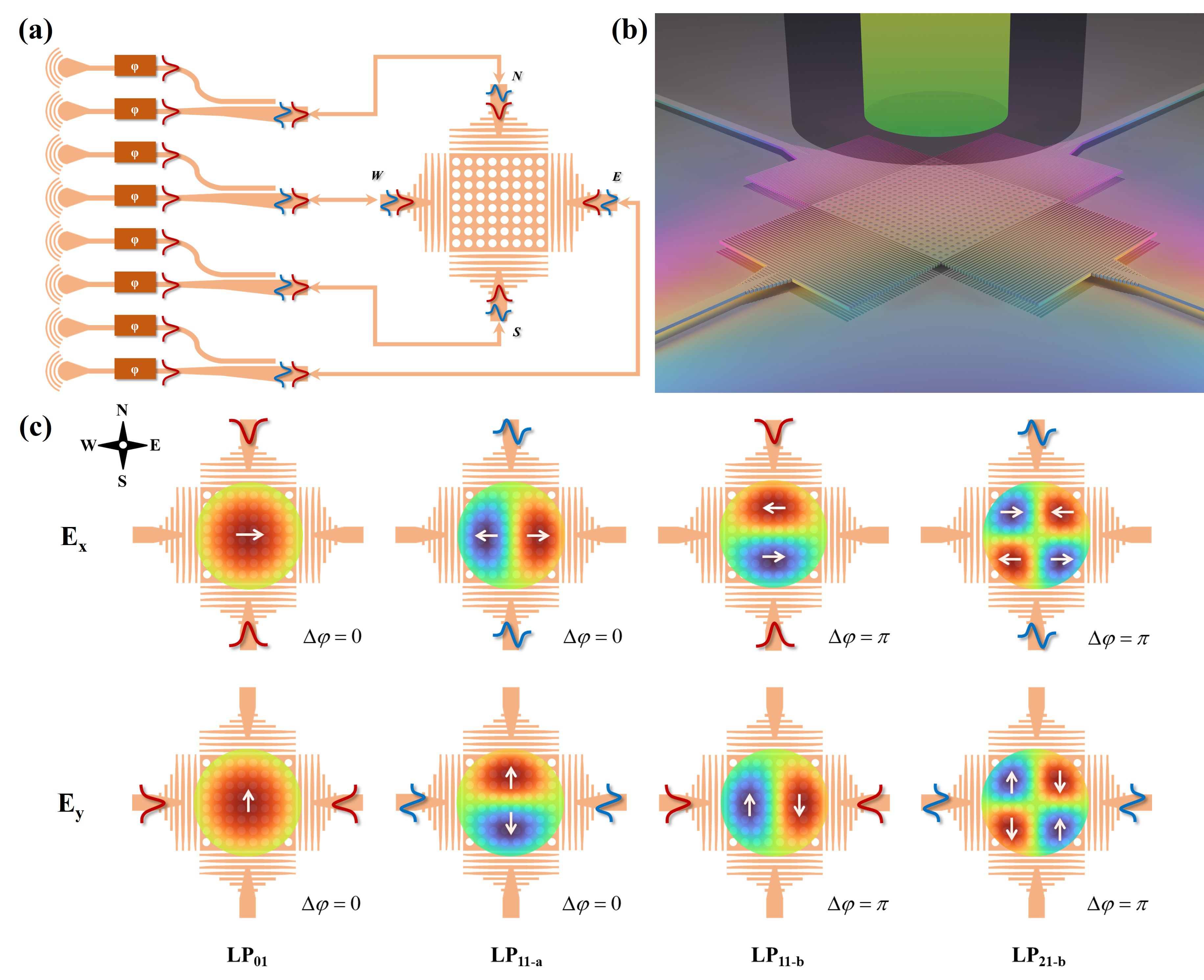
The proposed integrated mode DE/MUX for FMF is composed of a 2D multimode grating coupler (MMGC), four mode-size converters (MSCs), and four tapered adiabatic directional couplers (ADCs) as depicted in Figure 1a. Tapered ADCs are utilized for on-chip mode de/multiplexing of the TE0 mode and TE1 mode [41, 42] (see Supporting Information S1). Additionally, heater-based optical phase shifters are also necessary for selective mode excitation as a mode MUX. Intrinsic to its design, the 2D MMGC shown in Figure 1b serves as both a polarization combiner in the mode MUX and a polarization splitter in the mode DEMUX.
The selective mode launching of LP modes is depicted in Figure 1c, which can be explained as follows: The mode field profile of the LP01 mode in a FMF has only one maximum intensity point. A 2D grating coupler can be utilized to diffract the fundamental quasi transverse-electric mode (TE0) in the four orthogonally placed waveguides. By using the two counterpropagating TE0 modes in the same polarization with no relative phase difference, LP01 modes can be selectively excited. For the higher-order fiber modes, e.g. LP11 and LP21 modes, additional relative phase shift is required to match the diffracted optical field with the field distribution in FMF. As illustrated in Figure 1c, LP11a-x mode can be excited by the TE1 modes from south and north with no relative phase delay allowing the spots to be merged; LP11b-x can be obtained by the TE0 modes from south and north with a relative phase shift of . Similarly, LP11a-y and LP11b-y can be selectively launched using the TE0 and TE1 modes from west and east with appropriate phase shifts. For the LP21 mode group, LP21b-x mode can be excited by the TE1 modes from south and north in the same phase state. TE1 modes from the west and east can be used for launching the LP21b-y mode. A total of eight spatial modes can thus be selectively coupled via the proposed 2D MMGC.
The same design configuration can also be used as a mode DEMUX in the future. Selective decoupling only occurs when the fiber LP modes are of high modal purity and polarizations are precisely aligned. However, in practical scenarios, mode evolution of the LP modes and polarization rotation cannot be avoided in a circular-core FMF. As a result, unpredictable field patterns are generated at the fiber-to-chip coupling end [26, 36]. Nevertheless, for a two-mode FMF, our proposed design can receive all the degenerate modes in LP01 and LP11 group and convert them into 8 single-mode spatial channels on chip with preserved optical energy. While polarization crosstalk and modal crosstalk can result in signal degradation, it is possible to mitigate this issue through digital MIMO signal processing [43] or the use of Mach-Zehnder interferometer (MZI) meshes [44], as demonstrated in previous studies.
.1 Multimode Grating Coupler Design
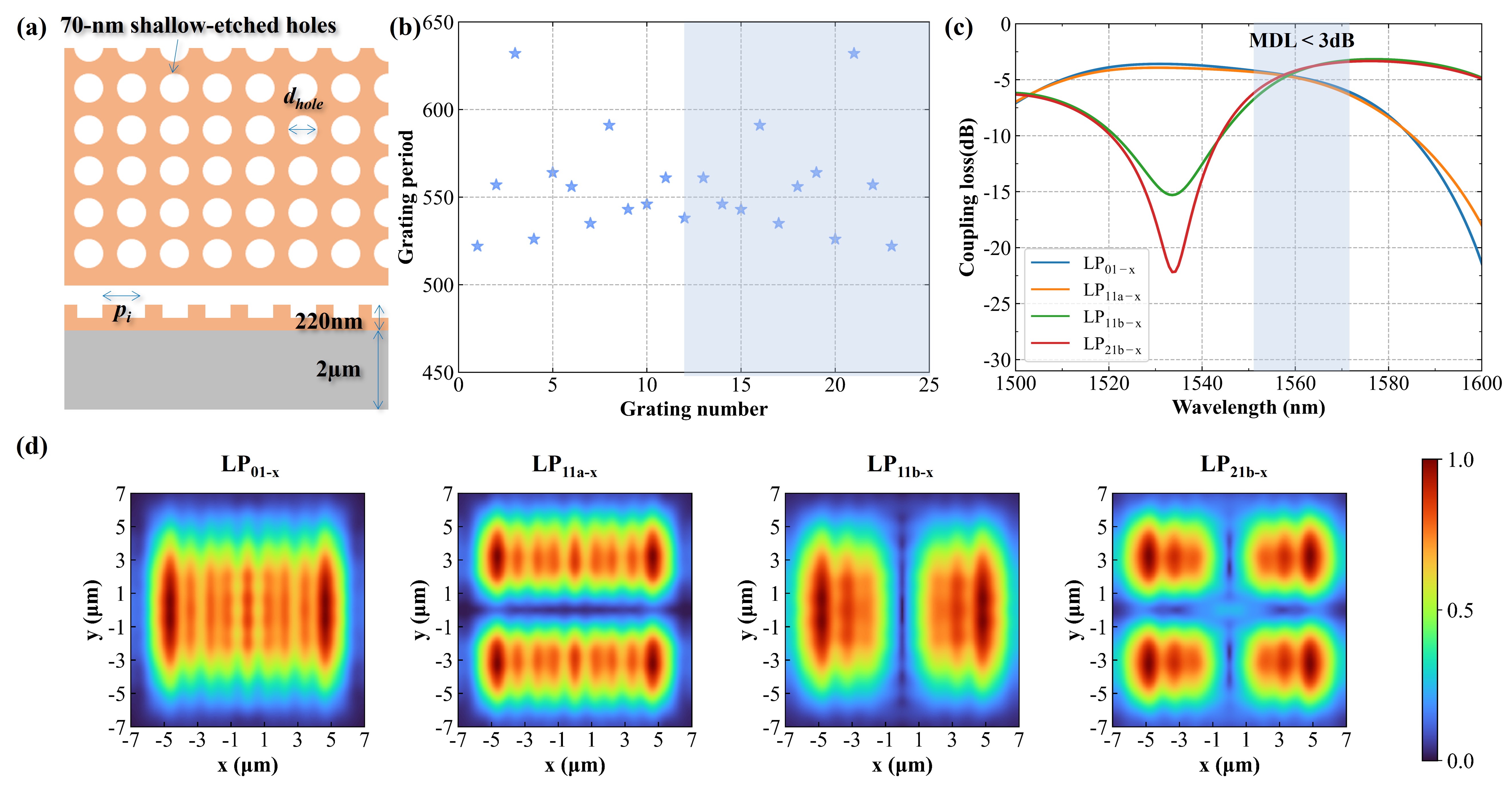
The proposed multimode grating is efficient for both TE0 and TE1 modes due to their comparable effective indices in the wide slab waveguide, which has a width exceeding 10 m. Our design utilizes a completely vertical coupling approach to decrease spatial dependent loss and eliminate angled fiber polishing. To make sure that the performance is consistent for all modes coming from the four slab waveguides in various directions, the design utilizes a symmetrical structure. As presented in Figure 2a, the SOI wafer comprises a top silicon layer with a thickness of 220 nm and a buried-oxide layer with a thickness of 2 m. A shallow etching process with a depth of 70 nm is used to create subwavelength holes as the low-index region in the grating, and a full etching process is needed later to make the strip waveguides.
It is known that grating couplers usually have a small coupling angle with respect to the chip surface normal to avoid second-order Bragg reflection into the waveguides. As a result, advanced designs such as chirped gratings [45, 46], are necessary for achieving efficient and perfectly vertical coupling. However, optimizing the chirping conditions for a 2D grating coupler is challenging. The 3D finite element simulations must consider the large fiber core and cladding as well as the sub-wavelength holes, making them computationally intensive. Estimating the figure-of-merit (FOM) of different fiber modes requires significant computing resources, which makes it difficult for optimization algorithms to converge.
To solve this problem, effective medium theory (EMT) was used to simplify the modelling into a 2D finite element simulation. While 2D simulations cannot accurately evaluate the coupling efficiencies for all fiber modes in the two orthogonal polarizations, they can easily obtain the coupling performance of the fundamental TE mode, which is sufficient for evaluating the FOM during the optimization process. Essentially, the MMGC is wide and symmetric for the two orthogonal polarizations, thus all the TE0 and TE1 modes in the orthogonal polarizations should exhibit similar or equivalent effective indices. Assuming good mode size matching, the coupling performance of the higher order fiber modes should be directly proportional to the results of the fundamental mode in 2D simulations. As a result of this, the computing resources needed to evaluate the FOM can be greatly reduced, making it possible for more sophisticated optimization algorithms, such as genetic algorithm in this work, to search the best design parameters. The second order EMT can be found in Supporting Information S2.
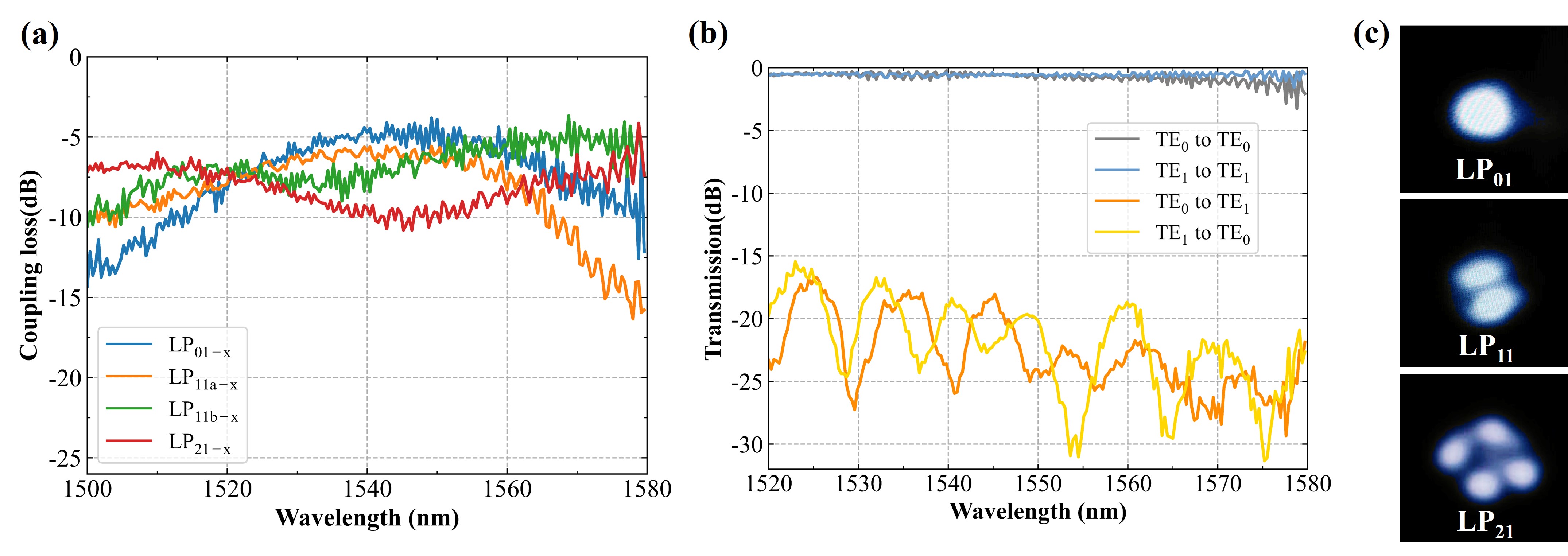
Figure 2b presents the length of each grating period with a constant etched hole diameter dhole of 343 nm. Performance of the chirped MMGC is verified using 3D finite-difference time-domain (FDTD) simulation. By configuring the appropriate phase shift as depicted in Figure 1c, the proposed MMGC can selectively excite various fiber LP modes. Figure 2c shows the coupling loss spectra for different x-polarized LP modes. The symmetrical design guarantees equivalent performance for the LP mode in the y polarization. LP01 and LP11a mode have a minimum coupling loss of -3.61 dB and -3.94 dB at a center wavelength of 1532 nm, with a 1-dB spectral bandwidth of about 47 nm. The minimum coupling loss for LP11b mode and LP21b mode are -3.17 dB and -3.75 dB, at 1577 nm respectively. The 1-dB spectral bandwidth for LP11b mode and LP21b mode are around 35 nm. The mode-dependent loss difference is less than 3 dB for all spatial mode channels over 21 nm spectral bandwidth from 1551 nm to 1572 nm. It’s worth noting that the peak coupling efficiencies of the four spatial channels have a relative wavelength shift of about 45 nm, which is mainly due to the fact that the optimal mode overlap integrals are obtained at different wavelengths for various modes.
Because of the arbitrary LP mode evolution from the coherent sum of the vectorial fiber modes and polarization rotation in a circular-core FMF, the field pattern arriving at the FMF end is always uncertain. Therefore, the received field pattern by grating coupler cannot be assumed as a pure LP mode with a perfectly aligned polarization. Nevertheless, our proposed MMGC can convert all the vectorial fiber modes in a two-mode FMF including HE11-x, HE11-y, TM01, TE01, HE21-even, HE21-odd into TE0 and TE1 mode on chip. Hence, optical pattern generated by the linear superposition of those vectorial modes at the fiber end can always be coupled and collected using the eight on-chip single-mode waveguides for signal descrambling. Such unique property is confirmed in 3D-FDTD simulation by launching various vectorial mode patterns in a 2-mode FMF and summing the received power on chip (see Supporting Information S3), the obtained coupling efficiencies agree well with the prior chip-to-fiber simulation performance.
.2 Mode Independent Mode Size Converter Design
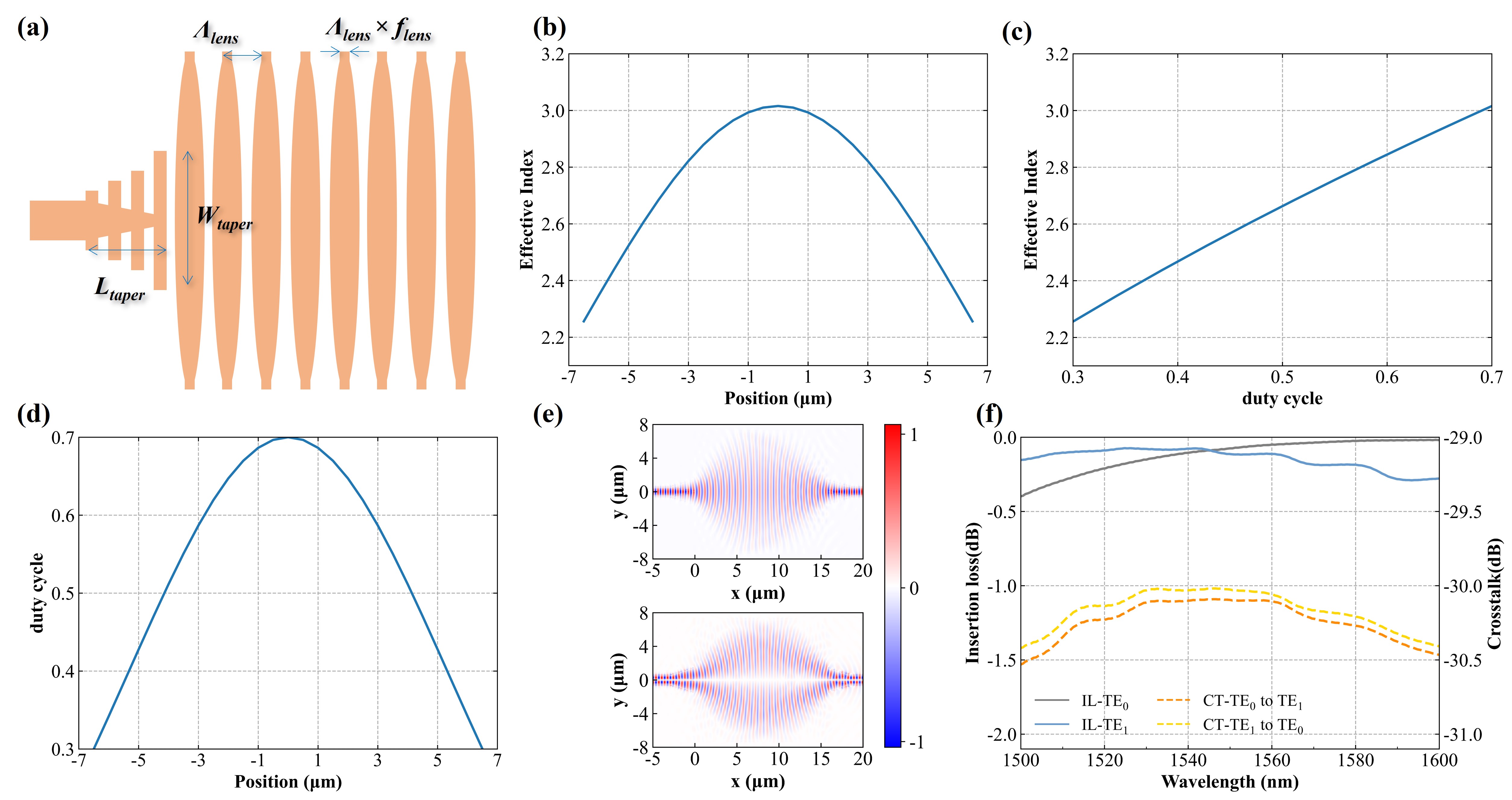
The large refractive index contrast of the SOI platform allows for effective confinement of optical modes within the silicon waveguides, enabling an extremely high level of integration density. Nevertheless, the mode field size also varies considerably between optical fibers and silicon channel waveguides. The highly confined waveguide modes with a typical mode field diameter of is not matched with fiber mode with a typical mode field diameter of . A long adiabatic linear taper is typically required for mode size conversion. In our case, a linear waveguide taper with a length of 350 m is necessary to minimize the transition loss for both the TE0 and TE1 modes. The taper length cannot be shortened without violating the adiabatic transition condition. The use of four linearly tapered MSCs for the proposed DE/MUX would cause a large device footprint and waste a lot of valuable chip area.
A compact and mode-independent mode size converter is thus a key step to improve the integration density. Mikaelian lens developed from Maxwell’s fish-eye lens using conformal transformation optics, is inherently free of spherical aberrations. Such unique property enables both paraxial and nonparaxial light to be focused at the same point using a single lens, making it perfectly suitable for mode-independent field size conversion. A compact integrated Mikaelian lens on photonic chip can be realized by using the subwavelength grating structures, which have already been widely exploited for many integrated photonic components [31, 32, 33, 34, 35].
The schematic of subwavelength Mikaelian lens is depicted in Figure 3a. By changing the duty cycle (defined by the ratio of silicon width to grating period) of the subwavelength silicon gratings, the effective refractive index is manipulated to form a desired refractive index profile of a Mikaelian lens shown in Figure 3b.
The subwavelength Mikaelian lens is designed to have a width of 13 m to match with the mode field diameter of the graded-index FMF. The maximum effective index nmax is 3.0158 in the center of the subwavelength gratings while the minimum effective index nmin is 2.2560 at the edge. The subwavelength grating pitch is set as 240 nm while the duty cycle varies continuously from 0.3 to 0.7. To map the effective index profile efficiently, the second order EMT is applied (see Supporting Information S2). Figure 3c presents the predicted effective index of the subwavelength grating against duty cycle. Effective index profile of the Mikaelian lens can thus be mapped to the duty cycles of the subwavelength gratings as presented in Figure 3d. A compact subwavelength Mikaelian lens is thus formed for mode-independent size conversion. To mitigate the reflection loss induced by the disparityu in effective indices between the subwavelength lens and the channel waveguide, a subwavelength taper was incorporated at the beginning of the Mikaelian lens in Figure 3a. The width and length of the subwavelength taper are fine-tuned to 2.5 m and 3.6 m, respectively to minimize the loss.
Figure 3e shows the simulated optical field profiles of the designed subwavelength Mikaelian lens back-to-back working for TE0 and TE1 modes. A compact and mode-independent field size conversion can be observed. The corresponding transmission spectra and inter-modal crosstalk are summarized in Figure 3f. A peak conversion efficiency of -0.02 dB and -0.07 dB can be obtained for the TE0 and TE1 modes, respectively. Meanwhile, the inter-modal crosstalk is below -30 dB over the whole C band.
Fabrication and Experimental Results
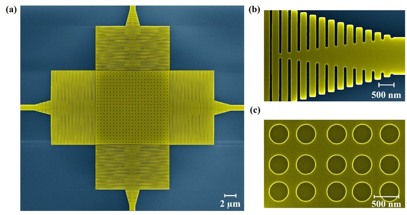
The proposed integrated multimode DE/MUX is fabricated on SOI wafer with a 220 nm thick top silicon layer. The buried-oxide layer has a thickness of 2 m. Electro-beam lithography is used to define the device patterns, followed by dry reactive-ion etching process with a shallow etch depth of 70 nm and a full etch. Silicon dioxide (SiO2) with a thickness of 1.2 m is used as the top cladding to protect the passive photonic circuits. Metallization is performed using high-resistance titanium-tungsten alloy (TiW) for local heat generation and aluminum for electrical signal routing. A 300-nm thick SiO2 passivation layer is used and selectively etched later to create windows over the aluminum pads for probing.
Scanning electron microscope (SEM) images of the fabricated MMGC and MSCs are presented in Figure 4a-c. The total footprint in Figure 4a is only 35×35 m2. Compared with the case by using the linear adiabatic tapers (713×713 m2) shown in the Figure S4a, the total footprint can be reduced by more than 400-fold.
| Ref. | Multimode fiber type | Num. of spatial channels | Experimental minimum coupling loss [dB] | Mode dependent loss [dB] | Footprint [MMGs and MSCs] m2 |
|---|---|---|---|---|---|
| [20] | Rectangular core | 4 | TE00-TE30: <-5.5 dB | < 2.5 dB | - |
| [21] | Circular core | 6 | LP01-LP11 <-20 dB | 5 dB | - |
| [22] | Circular core | 6 | - | < 2 dB | - |
| [25] | Circular core | 4 | LP01: -4.9 dB and LP11a: -6.1 dB | 630×630 | |
| [26] | Circular core | 6 | LP01: -5.2 dB, LP11: -9.0 dB and | >200×200 | |
| This work | Circular core | 8 | LP01: -3.8 dB, LP11a: -5.5 dB, LP11b: -3.6 dB and LP21b: -4.1 dB | Wavelength dependent | 35×35 |
The coupling loss of the fabricated MMGC was characterized by measuring the fiber-chip-fiber transmission using a tunable continuous-wave laser source and a power meter. A SMF with single-mode grating coupler is used at the input side. The polarization of the input mode was aligned by a three-paddle mechanical polarization controller so that all the transmission for x-polarization is maximized. An integrated Y-branch is used as the 50:50 power splitter, followed by 150-µm long waveguide heaters for phase tuning. The optical signals are sent to the ADCs, MSCs and MMGC with a 4-mode FMF at the output to collect optical power. The heater injection current of the TE0 mode can be tuned to maximize the transmission at 1550 nm or 1570 nm, to selectively launch LP01 or LP11b, respectively. Similarly, LP11 and LP21b can be selectively excited using the TE1 mode by the same approach. Figure 5a shows the normalized coupling loss spectra of the MMGC using a four-mode FMF. LP01 and LP11a have a peak coupling efficiency of -3.8 dB and -5.5 dB at 1549 nm and 1542 nm, respectively. LP11b and LP21b have a peak coupling efficiency of -3.6 dB and -4.1 dB at 1578nm and 1569nm respectively. The observed 1-dB spectral bandwidth is about 20 nm for all the spatial channels, which is narrower than the simulation results. It is mainly due to that the relative phase shift is only optimized for the center wavelength when performing the wavelength scan. Hybrid modes are thus excited at the edges of the wavelength scanning range. The presence of mode dependent loss can lead to a decrease of the transmission power and the spectral bandwidth, correspondingly.
The insertion loss and crosstalk of the integrated subwavelength Mikaelian lens are also characterized by measuring the fiber-chip-fiber transmission. Due to the low insertion loss of the proposed MSC, four Mikaelian lens connected back-to-back (see Figure S4b) are used to obtain the normalized insertion loss and crosstalk shown in Figure 5b. The measured minimum insertion loss of the TE0 and TE1 modes are -0.24 dB at 1540nm and -0.25 dB at 1573 nm, respectively. Inter-modal crosstalk levels can be well suppressed to less than -16 dB. The increased spectral ripples around 1570 nm are mainly due to limited sensitivity of our power meter when using the lossy single mode grating couplers, which are originally designed to be centered at 1545 nm.
To confirm the selective excitation of 8 spatial channels in FMF as illustrated in Figure 1c, we use an infrared camera with a 10× microscope objective to record the output field profile of the FMF. Figure 5c present the intensity profiles of the mode group LP01, LP11, and LP21, which confirms the selective launching ability of our design. Since the LP mode evolution and polarization rotation in a circular-core FMF are unpredictable, the FMF uses a three-paddle mechanical polarization controller to capture pure LP11 and LP21 at the fiber end as much as possible.
Table 1 summarizes integrated mode DE/MUX by the grating coupling approach for multimode fibers in the past decade. Compared with prior arts, our work for the first time shows an ultra-compact, efficient, and multichannel solution on chip to selectively launch 8 spatial channels in the FMF.
Conclusion
To summarize, an ultra-compact and efficient integrated multichannel mode multiplexer in silicon for few-mode fibers is demonstrated. Selectively launching of 8 spatial channels with a minimum coupling loss of -3.8 dB, -5.5 dB, -3.6 dB, -4.1 dB for LP01, LP11a, LP11b, and LP21b modes are demonstrated in experiment. Since a low coupling loss can be maintained for all the degenerate modes regardless of the mode or polarization change during transmission in a two-mode FMF, the proposed design can also work in a DEMUX where signal descrambling is required to eliminate modal crosstalk. More than that, the demonstrated design is very compact by using the subwavelength Mikaelian lens for mode independent field size conversion. The total footprint of the MMGC and MSCs can be shrunk by more than 400-fold to only 35×35 m2, paving the way for the densely integrated mode multiplexed systems.
Supporting Information: Supporting Information is available from the Wiley Online Library or from the author.
Acknowledgements: This work was funded by the Guangzhou-HKUST(GZ) Joint Funding Scheme 2023A03J0159, Start-up fund from the Hong Kong University of Science and Technology (Guangzhou) and Hong Kong RGC GRF grant 14203620. The authors acknowledge the Novel IC Exploration (NICE) Facility of HKUST(GZ) for device measurement and Applied Nanotools Inc. for device fabrication. Dr. Yi Wang and Mr. Yue Qin are acknowledged for technical assistance.
References
- [1] Richardson, D. J., Fini, J. M. & Nelson, L. E. Space-division multiplexing in optical fibres. Nature photonics 7, 354–362 (2013). URL https://www.nature.com/articles/nphoton.2013.94. Publisher: Nature Publishing Group.
- [2] Winzer, P. J. Making spatial multiplexing a reality. Nature Photonics 8, 345–348 (2014). URL https://www.nature.com/articles/nphoton.2014.58. Publisher: Nature Publishing Group UK London.
- [3] Puttnam, B. J., Rademacher, G. & Luís, R. S. Space-division multiplexing for optical fiber communications. Optica 8, 1186–1203 (2021). URL https://opg.optica.org/abstract.cfm?uri=optica-8-9-1186. Publisher: Optica Publishing Group.
- [4] Kobayashi, T. et al. 1-Pb/s (32 SDM/46 WDM/768 Gb/s) C-band dense SDM transmission over 205.6-km of single-mode heterogeneous multi-core fiber using 96-Gbaud PDM-16QAM channels. In 2017 Optical Fiber Communications Conference and Exhibition (OFC), 1–3 (IEEE, 2017). URL https://ieeexplore.ieee.org/abstract/document/7937146/.
- [5] Gregg, P. et al. Enhanced spin orbit interaction of light in highly confining optical fibers for mode division multiplexing. Nature communications 10, 4707 (2019). URL https://www.nature.com/articles/s41467-019-12401-4. Publisher: Nature Publishing Group UK London.
- [6] Velazquez-Benitez, A. M. et al. Six mode selective fiber optic spatial multiplexer. Optics letters 40, 1663–1666 (2015). URL https://opg.optica.org/abstract.cfm?uri=ol-40-8-1663. Publisher: Optica Publishing Group.
- [7] Gross, S., Riesen, N., Love, J. D. & Withford, M. J. Three-dimensional ultra-broadband integrated tapered mode multiplexers: Three-dimensional ultra-broadband integrated tapered mode multiplexers. Laser & Photonics Reviews 8, L81–L85 (2014). URL https://onlinelibrary.wiley.com/doi/10.1002/lpor.201400078.
- [8] Labroille, G. et al. Efficient and mode selective spatial mode multiplexer based on multi-plane light conversion. Optics express 22, 15599–15607 (2014). URL https://opg.optica.org/abstract.cfm?uri=oe-22-13-15599. Publisher: Optica Publishing Group.
- [9] Fontaine, N. K. et al. Laguerre-Gaussian mode sorter. Nature communications 10, 1865 (2019). URL https://www.nature.com/articles/s41467-019-09840-4. Publisher: Nature Publishing Group UK London.
- [10] Soma, D. et al. 10.16-Peta-B/s dense SDM/WDM transmission over 6-mode 19-core fiber across the C+ L band. Journal of Lightwave Technology 36, 1362–1368 (2018). URL https://ieeexplore.ieee.org/abstract/document/8274947/. Publisher: IEEE.
- [11] Rademacher, G. et al. Peta-bit-per-second optical communications system using a standard cladding diameter 15-mode fiber. Nature Communications 12, 4238 (2021). URL https://www.nature.com/articles/s41467-021-24409-w. Publisher: Nature Publishing Group UK London.
- [12] Rademacher, G. et al. 10.66 peta-bit/s transmission over a 38-core-three-mode fiber. In optical fiber communication conference, Th3H–1 (Optica Publishing Group, 2020). URL https://opg.optica.org/abstract.cfm?uri=OFC-2020-Th3H.1.
- [13] Liu, J. et al. 1-Pbps orbital angular momentum fibre-optic transmission. Light: Science & Applications 11, 202 (2022). URL https://www.nature.com/articles/s41377-022-00889-3. Publisher: Nature Publishing Group UK London.
- [14] Shi, W., Tian, Y. & Gervais, A. Scaling capacity of fiber-optic transmission systems via silicon photonics. Nanophotonics 9, 4629–4663 (2020). URL https://www.degruyter.com/document/doi/10.1515/nanoph-2020-0309/html.
- [15] Bogaerts, W. et al. Programmable photonic circuits. Nature 586, 207–216 (2020). URL https://www.nature.com/articles/s41586-020-2764-0. Publisher: Nature Publishing Group UK London.
- [16] Miller, D. A. Device requirements for optical interconnects to silicon chips. Proceedings of the IEEE 97, 1166–1185 (2009). URL https://ieeexplore.ieee.org/abstract/document/5071309/. Publisher: IEEE.
- [17] Zhao, W. et al. 96-Channel on-chip reconfigurable optical add-drop multiplexer for multidimensional multiplexing systems. Nanophotonics 11, 4299–4313 (2022). URL https://www.degruyter.com/document/doi/10.1515/nanoph-2022-0319/html.
- [18] Dai, D. & Bowers, J. E. Silicon-based on-chip multiplexing technologies and devices for Peta-bit optical interconnects. Nanophotonics 3, 283–311 (2014). URL https://www.degruyter.com/document/doi/10.1515/nanoph-2013-0021/html.
- [19] Tong, Y. et al. An experimental demonstration of 160-Gbit/s PAM-4 using a silicon micro-ring modulator. IEEE Photonics Technology Letters 32, 125–128 (2019). URL https://ieeexplore.ieee.org/abstract/document/8933415/. Publisher: IEEE.
- [20] Yang, K. Y. et al. Multi-dimensional data transmission using inverse-designed silicon photonics and microcombs. Nature Communications 13, 7862 (2022). URL https://www.nature.com/articles/s41467-022-35446-4. Publisher: Nature Publishing Group UK London.
- [21] Koonen, A. M. J., Chen, H., van den Boom, H. P. & Raz, O. Silicon photonic integrated mode multiplexer and demultiplexer. IEEE Photonics Technology Letters 24, 1961–1964 (2012). URL https://ieeexplore.ieee.org/abstract/document/6304909/. Publisher: IEEE.
- [22] Ding, Y., Ou, H., Xu, J. & Peucheret, C. Silicon photonic integrated circuit mode multiplexer. IEEE photonics technology letters 25, 648–651 (2013). URL https://ieeexplore.ieee.org/abstract/document/6461914/. Publisher: IEEE.
- [23] Wohlfeil, B. et al. A two-dimensional fiber grating coupler on SOI for mode division multiplexing. IEEE Photonics Technology Letters 28, 1241–1244 (2016). URL https://ieeexplore.ieee.org/abstract/document/7372392/. Publisher: IEEE.
- [24] Lai, Y. et al. Compact double-part grating coupler for higher-order mode coupling. Optics letters 43, 3172–3175 (2018). URL https://opg.optica.org/abstract.cfm?uri=ol-43-13-3172. Publisher: Optica Publishing Group.
- [25] Tong, Y., Zhou, W., Wu, X. & Tsang, H. K. Efficient mode multiplexer for few-mode fibers using integrated silicon-on-insulator waveguide grating coupler. IEEE Journal of Quantum Electronics 56, 1–7 (2019). URL https://ieeexplore.ieee.org/abstract/document/8886481/. Publisher: IEEE.
- [26] Watanabe, T. et al. Coherent few mode demultiplexer realized as a 2D grating coupler array in silicon. Optics Express 28, 36009–36019 (2020). URL https://opg.optica.org/abstract.cfm?uri=oe-28-24-36009. Publisher: Optica Publishing Group.
- [27] Shen, W., Du, J., Xiong, J., Ma, L. & He, Z. Silicon-integrated dual-mode fiber-to-chip edge coupler for 2\times 100 Gbps/lambda MDM optical interconnection. Optics Express 28, 33254–33262 (2020). URL https://opg.optica.org/abstract.cfm?uri=oe-28-22-33254. Publisher: Optica Publishing Group.
- [28] Zhang, W. et al. Low-crosstalk high-order mode silicon fiber-chip coupler by utilizing apodized double part gratings with mode selective trident. IEEE Photonics Journal 15, 1–4 (2023). URL https://ieeexplore.ieee.org/abstract/document/10050010/. Publisher: IEEE.
- [29] Zhou, X. & Tsang, H. K. High efficiency multimode waveguide grating coupler for few-mode fibers. IEEE Photonics Journal 14, 1–5 (2022). URL https://ieeexplore.ieee.org/abstract/document/9815878/. Publisher: IEEE.
- [30] Zhang, Y., He, Y., Zhu, Q., Qiu, C. & Su, Y. On-chip silicon photonic 2\times 2 mode-and polarization-selective switch with low inter-modal crosstalk. Photonics Research 5, 521–526 (2017). URL https://opg.optica.org/abstract.cfm?uri=prj-5-5-521. Publisher: Optica Publishing Group.
- [31] Cheben, P., Halir, R., Schmid, J. H., Atwater, H. A. & Smith, D. R. Subwavelength integrated photonics. Nature 560, 565–572 (2018). URL https://www.nature.com/articles/s41586-018-0421-7. Publisher: Nature Publishing Group UK London.
- [32] Luque-González, J. M. et al. An Ultracompact GRIN-Lens-Based Spot Size Converter using Subwavelength Grating Metamaterials. Laser & Photonics Reviews 13, 1900172 (2019). URL https://onlinelibrary.wiley.com/doi/10.1002/lpor.201900172.
- [33] Liu, Y. et al. Arbitrarily routed mode-division multiplexed photonic circuits for dense integration. Nature communications 10, 3263 (2019). URL https://www.nature.com/articles/s41467-019-11196-8. Publisher: Nature Publishing Group UK London.
- [34] Zhang, Z., Tong, Y., Wang, Y. & Tsang, H. K. Nonparaxial mode-size converter using an ultracompact metamaterial Mikaelian lens. Journal of Lightwave Technology 39, 2077–2083 (2020). URL https://ieeexplore.ieee.org/abstract/document/9306815/. Publisher: IEEE.
- [35] Xiang, J. et al. Metamaterial-enabled arbitrary on-chip spatial mode manipulation. Light: Science & Applications 11, 168 (2022). URL https://www.nature.com/articles/s41377-022-00859-9. Publisher: Nature Publishing Group UK London.
- [36] Kreysing, M. et al. Dynamic operation of optical fibres beyond the single-mode regime facilitates the orientation of biological cells. Nature communications 5, 5481 (2014). URL https://www.nature.com/articles/ncomms6481. Publisher: Nature Publishing Group UK London.
- [37] Xavier, G. B. & Lima, G. Quantum information processing with space-division multiplexing optical fibres. Communications Physics 3, 9 (2020). URL https://www.nature.com/articles/s42005-019-0269-7. Publisher: Nature Publishing Group UK London.
- [38] Carolan, J. et al. Universal linear optics. Science 349, 711–716 (2015). URL https://www.science.org/doi/10.1126/science.aab3642.
- [39] Čižmár, T. & Dholakia, K. Exploiting multimode waveguides for pure fibre-based imaging. Nature communications 3, 1027 (2012). URL https://www.nature.com/articles/ncomms2024. Publisher: Nature Publishing Group UK London.
- [40] Wan, N. H. et al. High-resolution optical spectroscopy using multimode interference in a compact tapered fibre. Nature communications 6, 7762 (2015). URL https://www.nature.com/articles/ncomms8762. Publisher: Nature Publishing Group UK London.
- [41] Ding, Y. et al. On-chip two-mode division multiplexing using tapered directional coupler-based mode multiplexer and demultiplexer. Optics express 21, 10376–10382 (2013). URL https://opg.optica.org/abstract.cfm?uri=oe-21-8-10376. Publisher: Optica Publishing Group.
- [42] Dai, D., Wang, J. & Shi, Y. Silicon mode (de) multiplexer enabling high capacity photonic networks-on-chip with a single-wavelength-carrier light. Optics letters 38, 1422–1424 (2013). URL https://opg.optica.org/abstract.cfm?uri=ol-38-9-1422. Publisher: Optica Publishing Group.
- [43] Ryf, R. et al. Mode-division multiplexing over 96 km of few-mode fiber using coherent 6\times 6 MIMO processing. Journal of Lightwave technology 30, 521–531 (2012). URL https://opg.optica.org/abstract.cfm?uri=jlt-30-4-521. Publisher: IEEE.
- [44] Annoni, A. et al. Unscrambling light—automatically undoing strong mixing between modes. Light: Science & Applications 6, e17110–e17110 (2017). URL https://www.nature.com/articles/lsa2017110. Publisher: Nature Publishing Group.
- [45] Chen, X., Li, C. & Tsang, H. K. Fabrication-tolerant waveguide chirped grating coupler for coupling to a perfectly vertical optical fiber. IEEE Photonics Technology Letters 20, 1914–1916 (2008). URL https://ieeexplore.ieee.org/abstract/document/4607244/. Publisher: IEEE.
- [46] Tong, Y., Zhou, W. & Tsang, H. K. Efficient perfectly vertical grating coupler for multi-core fibers fabricated with 193 nm DUV lithography. Optics Letters 43, 5709–5712 (2018). URL https://opg.optica.org/abstract.cfm?uri=ol-43-23-5709. Publisher: Optica Publishing Group.