Shortcomings of using the SCAN functional for point defects and polarons in semiconductors
Abstract
We find the recently developed strongly constrained and appropriately normalized (SCAN) functional, now widely used in calculations of many materials, is not able to reliably describe the properties of deep defects and small polarons in several semiconductors and insulators. These shortcomings are due to a failure to identify the large structural distortions and charge localization that accompanies the presence of defects and the formation of small polarons. Our results indicate the SCAN functional is insufficient to yield quantitative and qualitatively accurate results for defect calculations.
Density functional theory (DFT) calculations using supercells are the workhorse method for investigating dopants and defects in semiconductors [1]. These studies play a central role in defect identification and also in guiding the discovery of new materials and strategies to control their conductivity. Some examples of this include calculations of point defects in III-nitrides for optoelectronics [2], transparent conducting oxides [3] to defects in wide-band gap semiconductors for quantum information science [4, 5].
This success is due in part to the development and application of advanced functionals such as the Heyd-Scuseria, and Ernzerhof (HSE) [6, *HeydJCP2006] hybrid functional, which reduces the amount of self-interaction error that is inherent to semi-local functionals. Self-interaction errors lead to underestimated band gaps and a tendency to delocalize charge density [8], precluding an accurate description of charge localization and local lattice distortions, which are pertinent in the context of defect calculations. However, the large computational expense of hybrid functionals limits their widespread use for large system sizes. One approach to overcome this is to rely on functionals that improve upon the shortcomings of traditional functionals such as the generalized gradient approximation (GGA) and local density approximation (LDA) without incurring large computational costs. A prominent example is the recently developed strongly constrained and appropriately normed (SCAN) functional [9], which has been shown to have less self-interaction error compared to the GGA and LDA functionals [10].
Naturally, this motivates the question on whether the SCAN functional can be reliably applied to investigate the properties of defects in semiconductors. Indeed, numerous studies have begun to explore this question [11, 12, 13, 14, 15, 16, 17, 18]. For the calculation of defect transition levels, a popular approach has been optimizing the structure with the SCAN functional and then performing a single shot (i.e., no atomic relaxations) self-consistent calculation with the HSE functional [15], while other studies have relied on a forthright application of SCAN to determine the atomic geometry and total energies [14, 11, 12, 13]. These approaches assume the local distortions due to the defect in a given charge state are correctly captured with SCAN. SCAN has also been applied successfully to determine intra-defect transition energies and optical lineshapes of defects [17, 18]. However, the success of this approach is predicated on the single particle states of the defect residing within the gap, combined with the fact that SCAN yields reliable lattice dynamics for a wide range of materials [19]. The overall consensus from these studies has been in favor of applying the SCAN functional as a reliable means to study defects in semiconductors.
While SCAN leads to an encouraging improvement over GGA and LDA in the description of semiconductors, in this paper we scrutinize a set of critical issues that have not been considered when applying the SCAN functional to the investigation of deep-level defects and small polarons. Deep defects are characterized by a transition level that is located in the gap (at an energy that makes room-temperature ionization unlikely) and a wavefunction that is localized on the length scale of an atomic bond. A small polaron forms when an excess charge carrier in a semiconductor or insulator introduces a lattice distortion that is large enough to lead to charge localization often around a single atomic site. We focus on five diverse defects that allow us to highlight the importance of charge localization and symmetry-breaking structural distortions aspects that are germane to the study of deep defects and small polarons in all gapped materials. The defects we will investigate are: substitutional calcium acceptors (CaGa) in GaN, substitional carbon acceptors (CN) in GaN, the zinc vacancy () in ZnO, substitutional magnesium acceptors (MgGa) in -Ga2O3 and the self-trapped hole (hole polaron) in NaF. Each of these candidate defects have been identified in experiment, which allows us to benchmark our SCAN and HSE calculations.
We find that while SCAN does identify deep transition levels in the gap compared to GGA, it completely fails to identify local structural distortions or describe charge localization. Based on these insights, we recommend that defect and doping studies that are based on the popular SCAN functional must be interpreted with caution.
We begin by examining the bulk properties of GaN, ZnO, Ga2O3 and NaF obtained using our first-principles calculations [20]. Table 1 compares the lattice parameters and band gap of these compounds obtained using the PBE, SCAN and HSE functionals, as well as experimental values.
| Material | Lattice parameters (Å) | Band gap (eV) | ||||||
| PBE | SCAN | HSE | Expt. | PBE | SCAN | HSE | Expt. | |
| ZnO | a=3.28,c=5.28 | a=3.23,c=5.21 | a=3.24,c=5.19 | a=3.25,c=5.21 | 0.76 | 1.21 | 3.42 | 3.43 |
| GaN | a=3.22,c=5.22 | a=3.19,c=5.23 | a=3.19,c=5.17 | a=3.19,c=5.19 | 1.57 | 2.22 | 3.49 | 3.50 |
| Ga2O3 | a=12.44,b=3.08, c=5.92 | a=12.09,b=3.04, c=5.82 | a=12.21,b=3.03, c=5.80 | a=12.21,b=3.04, c=5.80 | 2.25 | 2.77 | 4.86 | 4.48-4.90 |
| NaF | a=4.62 | a=4.47 | a=4.56 | a=4.57 | 6.51 | 7.25 | 11.20 | 11.50 |
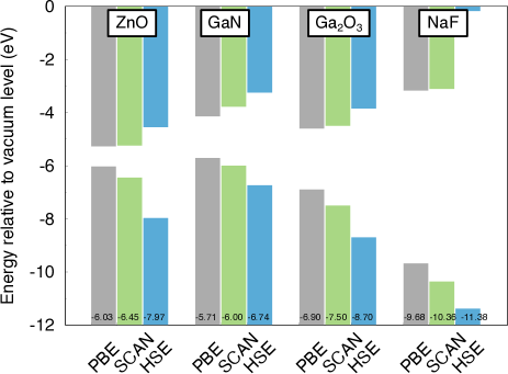
SCAN yields structural parameters that are in remarkably good agreement with experiment, and leads to band gaps that are improved compared to PBE, but still underestimated compared to experiment. For defect calculations, the absolute position of band edges is as important as the magnitude of the predicted band gap [27]. In Fig. 1, we illustrate the absolute position of the band edges for each of the compounds.
Since SCAN improves upon the description of band gaps and band edges compared to GGA, it does lead to charge-state transition levels in the gap for the four defects we investigate (whereas some of these defects are predicted to be shallow with GGA). However, when scrutinizing the details of the SCAN calculations and comparing with HSE we notice several key differences, which we comment on below.
The first case study is in ZnO. Prior HSE calculations [28, 29] have shown in ZnO exhibits a (2+/+) level at +0.25 eV, a (+/0) level at +0.91 eV, a (0/) level at +1.45 eV and a (/2) level at +1.92 eV, where is the ZnO valence-band maximum (VBM). With SCAN, we find only the 0, and 2 charge states are stable in the gap, with the (0/) level at +0.25 eV and the (/2) level at +0.51 eV. Furthermore, electron-paramagnetic resonance experiments [30] have suggested that each of the oxygen dangling bonds that are nearest neighbor to the site can host a localized hole state. This is corroborated by our HSE calculations illustrated in Fig. 2(a), where we show holes localized on two of the oxygen dangling bonds in the neutral charge state of , consistent with the two electrons that can fill the Zn vacancy. Localizing the density on each oxygen atom is also accompanied by a reduction in the Zn-O bond lengths at the O atoms where charge is localized. In contrast, SCAN delocalizes the charge density of the two empty states across multiple O atoms as illustrated in the isosurface plot in Fig. 2(a) for the neutral charge state of in ZnO. This failure to describe charge localization also results in lower lattice distortions of the O atoms in the vicinity of the Zn vacancy site.
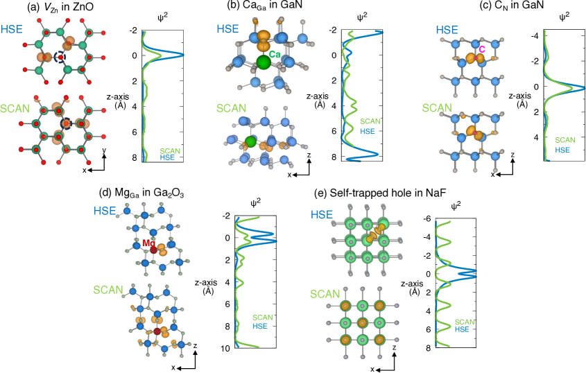
The second case study is the CaGa impurity in GaN. It is a deep acceptor [31] and has recently been identified as an efficient nonradiative recombination center in GaN [32, 33]. Both HSE and SCAN identify CaGa as a deep acceptor: the (0/) level is at +0.73 eV with SCAN, and it is at +1.06 eV using HSE (again, is the GaN VBM). With HSE, we find CaGa in the neutral charge state exhibits a large asymmetric distortion; the axial Ca-N bond length is 17% longer than the equilibrium Ga-N bond length, which localizes the hole on the axial N atom that is nearest neighbor to CaGa. Hole localization and large asymmetric distortions have been identified in the case of other group-II acceptors on the Ga site in GaN using HSE calculations [34]. With SCAN, the nearest neighbor Ca-N bonds are symmetrically distorted in the neutral charge state, even if one starts from the HSE geometry with the asymmetric distortion. Consequently, the hole state is delocalized across multiple nitrogen lattice sites for the calculations done with SCAN, as illustrated in Fig. 2(b).
The third case study is the CN impurity in GaN, which has been established as a deep acceptor [35, 36]. HSE calculations find the (0/) level at +1.02 eV and with SCAN the (0/) level is more shallow at +0.64 eV. The hole state that arises from CN is composed of C orbitals, which we find in the gap in both HSE and SCAN calculations as illustrated in Figure 2(c). Note there is some delocalization of the charge density towards the second nearest neighbor N atoms predicted with SCAN. While both functionals show CN acts as an atomic-like deep acceptor with the defect state derived from the impurity itself, there are key differences in the local lattice relaxation around the carbon impurity site. With HSE, we find an asymmetric relaxation of the nearest neighbor C-Ga bonds in the neutral charge state, with one of the basal plane C-Ga bonds increasing by 6% relative to the equilibrium Ga-N bond length and the remaining three C-Ga bonds increasing by 1%. With SCAN, we find lower and symmetric distortions in the neutral charge state; the four nearest neighbor C-Ga bond lengths increase by 1.5% relative to the equilibrium Ga-N bond length. In the negative charge state the relaxation is similar between HSE and SCAN, in both cases the four C-Ga bonds decrease in length by 1%.
The fourth case study is the MgGa impurity which is a deep acceptor in Ga2O3 [37]. This is confirmed by both HSE and SCAN calculations. The (0/) level is at +1.45 eV using HSE, which is close to the experimental value of 1.2 eV [37]. With SCAN, the (0/) level is only at +0.45 eV. Mg is a polaronic acceptor since the hole is localized primarily on an oxygen atom that is a nearest-neighbor to the MgGa site, and this is also accompanied by a large lattice distortion of this Mg-O bond. This hole localization, which is captured in our HSE calculations [Fig. 2(d)], is in agreement with electron-paramagnetic resonance experiments [38] that identified evidence for hole trapping on the oxygen site due to MgGa. Hole localization at deep acceptors accompanied by large lattice distortions is a characteristic feature of several oxide semiconductors, and has proven to be crucial to understand the electrical and optical properties of this important class of materials [39, 40]. The SCAN calculations lead to a lower lattice distortion in the vicinity of MgGa, and the hole in the neutral charge state is delocalized across multiple oxygen sites, a similar situation with the case of CaGa in GaN.
The final case study is the self-trapped hole in NaF, which is an archetypal example of a small polaron. Experiments and theory [41, 42] have shown that when holes are introduced into NaF, they self trap to form small hole polarons which are accompanied by the displacement of two near-neighbor F atoms along the 110 direction towards each other. In our HSE calculations, we find the dimerization of two F atoms with a F-F bond length of 1.9 Å, with the hole localizing on both dimerized F atoms as illustrated in Figure 2(e). SCAN fails to stabilize the small polaron in NaF. It does not find the dimerization of the F atoms, and also delocalizes the wavefunction of the hole state across all of the F atoms within the supercell.
In the five case studies illustrated in Fig. 2, we find that though SCAN identifies deep thermodynamic transition levels (albeit with ionization energies that are underestimated compared to HSE), it systematically fails to describe charge localization of the defect states and fails to capture the large local structural distortions in the vicinity of the defect or polaron site. An accurate description of charge localization is essential to accurately predict a range of properties, which includes but is not limited to: electron-phonon coupling due to defects [43], radiative recombination coefficients [44] and hyperfine parameters [4]. The delocalized charge density associated with the defect states obtained with SCAN, will lead to inaccurate predictions from such calculations. It is worth reiterating that these features of charge localization and large local distortions are characteristic features of deep defects and small polarons in a wide range of semiconductors and insulators.
The inability to identify charge localization and large structural distortions impacts the coupling between the defect and the lattice. If the occupation of the defect level is changed either electrically or optically, or if there is a change in the configuration of a defect wavefunction within the same charge state (i.e., an intra-defect transition), the initial and final configurations often correspond to different geometries of the defect. These local distortions of the defect geometry manifest themselves experimentally and therefore serve as “fingerprints” that can be used to identify the microscopic origins of unknown defects. Coupling between the atomic and electronic structure of the defect is best understood using configuration coordinate diagrams and the Franck-Condon approximation as discussed in Ref. [45]. Briefly, in the context of an optical absorption measurement that involves a defect in a given charge state and photoionization to a band edge, within the Franck-Condon approximation the change in geometry associated with the change in charge state of the defect leads to a peak absorption energy that differs from the ionization energy of the defect. This difference in energies is referred to as the relaxation energy. Analogous arguments apply in the context of photoluminescence that involves a defect state and a band edge.
For example, for MgGa in Ga2O3, experiments identified the relaxation energy associated with photoionization from the neutral to the negative charge state of MgGa to be 1.3 eV, which is consistent with the relaxation energy of 1.1 eV we find in our HSE calculations of the configuration-coordinate diagram for this process illustrated in Fig. 3(a).
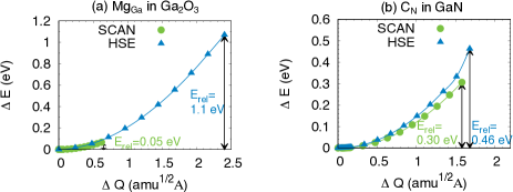
However, with SCAN the change in atomic geometry between the two charge states is significantly lower than what we find with HSE, and the corresponding relaxation energy (0.05 eV) is more than an order of magnitude lower.
We also examined the photoluminescence process involving CN in GaN where experiments [46] have shown a broad yellow luminescence band with a peak energy of 2.2 eV, which is in good agreement with HSE calculations that predict a peak emission energy of 2.14 eV and a large relaxation energy of 0.5 eV [36]. SCAN underestimates this relaxation energy, which we find to be 0.3 eV as illustrated in Fig. 3(b). This is due an underestimation in the lattice relaxation between the neutral and negative charge state of CN. Hence, in the context of using SCAN to analyze optical transitions due to these two defects, one would fail to describe the microscopic details such as the width of the optical spectra, even if the underestimated ionization energies were corrected in a post-processing step to match the HSE or experimental value.
Another pitfall with applying SCAN is the underestimation of defect ionization energies, which is due to the underestimated band gaps and incorrect position of band edges on an absolute scale. Previous studies corrected this by applying a Hubbard- correction to specific orbitals [47]. It might be tempting to conclude this provides a solution to the shortcomings with applying SCAN for defect calculations. A suitable test case is the defect in ZnO, where SCAN underestimates the ionization energies and leads to delocalized charge densities. This is due in part to the interaction of the filled Zn band with the O states of the valence band, which leads to a VBM that is too high on an absolute scale. Applying a Hubbard- of 5 eV to the Zn- states (consistent with GGA+ calculations of ZnO [48]) increases the SCAN+ ZnO band gap from 1.21 eV to 1.95 eV, lowers the VBM by 0.2 eV relative to the SCAN VBM, and increases the ionization energy of the (0/) and (/2) levels. However, we find this SCAN+ correction still leads to charge that is delocalized across multiple oxygen atoms in the neutral charge state, in contradiction with experiment and HSE calculations.
In conclusion, we examined the SCAN functional when applied to investigations of point defects and self-trapped holes (small polarons) in semiconductors and insulators, and compared our results with HSE hybrid functional calculations. For deep-level defects, the SCAN functional identifies thermodynamic transition levels in the gap. However, for each of the deep defects that we investigated, SCAN delocalizes the charge density of the defect state, fails to identify asymmetric structural relaxations, and underestimates the change in geometry due to the change in charge state. For self-trapped holes, SCAN fails to describe charge localization and the large lattice relaxation that accompanies the formation of these small polarons. We conclude that great care should be taken in interpreting the results of defect calculations using the SCAN functional.
Acknowledgements We acknowledge insightful discussions with Anderson Janotti and Chris Van de Walle. This work was supported by the Office of Naval Research through the Naval Research Laboratory’s Basic Research Program, and computations were performed at the DoD Major Shared Resource Centers at AFRL and the Army ERDC.
References
- Freysoldt et al. [2014] C. Freysoldt, B. Grabowski, T. Hickel, J. Neugebauer, G. Kresse, A. Janotti, and C. G. Van de Walle, First-principles calculations for point defects in solids, Rev. Mod. Phys. 86, 253 (2014).
- Lyons and Van de Walle [2017] J. L. Lyons and C. G. Van de Walle, Computationally predicted energies and properties of defects in GaN, npj Computational Mater. 3, 1 (2017).
- Willis and Scanlon [2021] J. Willis and D. O. Scanlon, Latest directions in p-type transparent conductor design, Journal of Materials Chemistry C 9, 11995 (2021).
- Ivády et al. [2018] V. Ivády, I. A. Abrikosov, and A. Gali, First principles calculation of spin-related quantities for point defect qubit research, npj Computational Materials 4, 76 (2018).
- Dreyer et al. [2018] C. E. Dreyer, A. Alkauskas, J. L. Lyons, A. Janotti, and C. G. Van de Walle, First-principles calculations of point defects for quantum technologies, Annual Review of Materials Research 48, 1 (2018).
- Heyd et al. [2003] J. Heyd, G. Scuseria, and M. Ernzerhof, Hybrid functionals based on a screened Coulomb potential, J. Chem. Phys. 118, 8207 (2003).
- Heyd et al. [2006] J. Heyd, G. E. Scuseria, and M. Ernzerhof, Erratum: “Hybrid functionals based on a screened Coulomb potential”, J. Chem. Phys. 124, 219906 (2006).
- Mori-Sánchez et al. [2008] P. Mori-Sánchez, A. J. Cohen, and W. Yang, Localization and delocalization errors in density functional theory and implications for band-gap prediction, Phys. Rev. Lett. 100, 146401 (2008).
- Sun et al. [2015] J. Sun, A. Ruzsinszky, and J. P. Perdew, Strongly constrained and appropriately normed semilocal density functional, Phys. Rev. Lett. 115, 036402 (2015).
- Peng and Perdew [2017] H. Peng and J. P. Perdew, Synergy of van der Waals and self-interaction corrections in transition metal monoxides, Phys. Rev. B 96, 100101 (2017).
- Sun et al. [2016] J. Sun, R. C. Remsing, Y. Zhang, Z. Sun, A. Ruzsinszky, H. Peng, Z. Yang, A. Paul, U. Waghmare, X. Wu, et al., Accurate first-principles structures and energies of diversely bonded systems from an efficient density functional, Nat. Chem. 8, 831 (2016).
- Rijal et al. [2021] B. Rijal, A. M. Z. Tan, C. Freysoldt, and R. G. Hennig, Charged vacancy defects in monolayer phosphorene, Phys. Rev. Mater. 5, 124004 (2021).
- Rushchanskii et al. [2021] K. Z. Rushchanskii, S. Blügel, and M. Ležaić, Ordering of oxygen vacancies and related ferroelectric properties in HfO2-δ, Phys. Rev. Lett. 127, 087602 (2021).
- Rauch et al. [2021] T. Rauch, F. Munoz, M. A. Marques, and S. Botti, Defect levels from SCAN and mBJ meta-GGA exchange-correlation potentials, Phys. Rev. B 104, 064105 (2021).
- Wexler et al. [2021] R. B. Wexler, G. S. Gautam, and E. A. Carter, Optimizing kesterite solar cells from Cu2ZnSnS4 to Cu2CdGe(S, Se)4, J. Mater. Chem. A 9, 9882 (2021).
- Han et al. [2022] D. Han, S. S. Rudel, W. Schnick, and H. Ebert, Self-doping behavior and cation disorder in MgSnN2, Phys. Rev. B 105, 125202 (2022).
- Maciaszek et al. [2023] M. Maciaszek, V. Žalandauskas, R. Silkinis, A. Alkauskas, and L. Razinkovas, The application of the SCAN density functional to color centers in diamond, J. Chem. Phys. 159, 084708 (2023).
- Ivanov et al. [2023] A. V. Ivanov, Y. L. A. Schmerwitz, G. Levi, and H. Jónsson, Electronic excitations of the charged nitrogen-vacancy center in diamond obtained using time-independent variational density functional calculations, SciPost Phys. 15, 009 (2023).
- Ning et al. [2022] J. Ning, J. W. Furness, and J. Sun, Reliable lattice dynamics from an efficient density functional approximation, Chem. Mater. 34, 2562 (2022).
- [20] See Supplemental Material at [url] for details on the electronic structure calculations which includes Refs.[48-53].
- Madelung [2012] O. Madelung, Semiconductors—basic data (Springer Science & Business Media, 2012).
- Maruska and Tietjen [1969] H. P. Maruska and J. Tietjen, The preparation and properties of vapor-deposited single-crystal-line GaN, Appl. Phys. Lett. 15, 327 (1969).
- Freitas Jr et al. [2001] J. Freitas Jr, G. Braga, W. Moore, J. Tischler, J. Culbertson, M. Fatemi, S. Park, S. Lee, and Y. Park, Structural and optical properties of thick freestanding GaN templates, J. Cryst. Growth 231, 322 (2001).
- Åhman et al. [1996] J. Åhman, G. Svensson, and J. Albertsson, A reinvestigation of -gallium oxide, Acta Crystallogr., Sect. C: Cryst. Struct. Commun 52, 1336 (1996).
- Onuma et al. [2015] T. Onuma, S. Saito, K. Sasaki, T. Masui, T. Yamaguchi, T. Honda, and M. Higashiwaki, Valence band ordering in -Ga2O3 studied by polarized transmittance and reflectance spectroscopy, Jpn. J. Appl. Phys. 54, 112601 (2015).
- Prencipe et al. [1995] M. Prencipe, A. Zupan, R. Dovesi, E. Apra, and V. Saunders, Ab initio study of the structural properties of LiF, NaF, KF, LiCl, NaCl, and KCl, Phys. Rev. B 51, 3391 (1995).
- Alkauskas et al. [2008] A. Alkauskas, P. Broqvist, and A. Pasquarello, Defect energy levels in density functional calculations: Alignment and band gap problem, Phys. Rev. Lett. 101, 046405 (2008).
- Frodason et al. [2017] Y. Frodason, K. Johansen, T. Bjørheim, B. Svensson, and A. Alkauskas, Zn vacancy as a polaronic hole trap in ZnO, Phys. Rev. B 95, 094105 (2017).
- Lyons et al. [2017] J. L. Lyons, J. B. Varley, D. Steiauf, A. Janotti, and C. G. Van de Walle, First-principles characterization of native-defect-related optical transitions in ZnO, J. Appl. Phys. 122, 035704 (2017).
- Evans et al. [2008] S. Evans, N. Giles, L. Halliburton, and L. Kappers, Further characterization of oxygen vacancies and zinc vacancies in electron-irradiated ZnO, J. Appl. Phys. 103, 043710 (2008).
- Shen et al. [2017] J.-X. Shen, D. Wickramaratne, C. E. Dreyer, A. Alkauskas, E. Young, J. S. Speck, and C. G. Van de Walle, Calcium as a nonradiative recombination center in InGaN, Appl. Phys. Express 10, 021001 (2017).
- Young et al. [2016] E. Young, N. Grandjean, T. Mates, and J. Speck, Calcium impurity as a source of non-radiative recombination in (In, Ga) N layers grown by molecular beam epitaxy, Appl. Phys. Lett. 109, 212103 (2016).
- Zhao et al. [2023] F. Zhao, M. E. Turiansky, A. Alkauskas, and C. G. Van de Walle, Trap-assisted Auger-Meitner recombination from first principles, Phys. Rev. Lett. 131, 056402 (2023).
- Lyons et al. [2013] J. L. Lyons, A. Janotti, and C. G. Van de Walle, Impact of group-II acceptors on the electrical and optical properties of GaN, Japanese J. Appl. Phys. 52, 08JJ04 (2013).
- Kanegae et al. [2021] K. Kanegae, T. Narita, K. Tomita, T. Kachi, M. Horita, T. Kimoto, and J. Suda, Photoionization cross section ratio of nitrogen-site carbon in GaN under sub-bandgap-light irradiation determined by isothermal capacitance transient spectroscopy, Appl. Phys. Express 14, 091004 (2021).
- Lyons et al. [2010] J. L. Lyons, A. Janotti, and C. G. Van de Walle, Carbon impurities and the yellow luminescence in GaN, Appl. Phys. Lett. 97, 152108 (2010).
- Bhandari et al. [2022] S. Bhandari, J. L. Lyons, D. Wickramaratne, and M. Zvanut, Optical transitions of neutral Mg in Mg-doped -Ga2O3, APL Mater. 10, 021103 (2022).
- Kananen et al. [2017] B. E. Kananen, L. E. Halliburton, E. M. Scherrer, K. Stevens, G. Foundos, K. Chang, and N. C. Giles, Electron paramagnetic resonance study of neutral mg acceptors in -Ga2O3 crystals, Appl. Phys. Lett. 111, 072102 (2017).
- Varley et al. [2012] J. B. Varley, A. Janotti, C. Franchini, and C. G. Van de Walle, Role of self-trapping in luminescence and p-type conductivity of wide-band-gap oxides, Phys. Rev. B 85, 081109 (2012).
- Lyons [2022] J. L. Lyons, Self-trapped holes and polaronic acceptors in ultrawide-bandgap oxides, J. Appl. Phys. 131, 025701 (2022).
- Williams and Song [1990] R. Williams and K. Song, The self-trapped exciton, J. Phys. Chem. Solids 51, 679 (1990).
- Miceli et al. [2018] G. Miceli, W. Chen, I. Reshetnyak, and A. Pasquarello, Nonempirical hybrid functionals for band gaps and polaronic distortions in solids, Phys. Rev. B 97, 121112 (2018).
- Turiansky et al. [2021] M. E. Turiansky, A. Alkauskas, M. Engel, G. Kresse, D. Wickramaratne, J.-X. Shen, C. E. Dreyer, and C. G. Van de Walle, Nonrad: Computing nonradiative capture coefficients from first principles, Comput. Phys. Commun. 267, 108056 (2021).
- Dreyer et al. [2020] C. E. Dreyer, A. Alkauskas, J. L. Lyons, and C. G. Van de Walle, Radiative capture rates at deep defects from electronic structure calculations, Phys. Rev. B 102, 085305 (2020).
- Alkauskas et al. [2016] A. Alkauskas, M. D. McCluskey, and C. G. Van de Walle, Tutorial: Defects in semiconductors—combining experiment and theory, J. Appl. Phys. 119, 181101 (2016).
- Ogino and Aoki [1980] T. Ogino and M. Aoki, Mechanism of yellow luminescence in GaN, Japanese J. Appl. Phys. 19, 2395 (1980).
- Long et al. [2020] O. Y. Long, G. S. Gautam, and E. A. Carter, Evaluating optimal U for 3d transition-metal oxides within the SCAN+U framework, Phys. Rev. Mater. 4, 045401 (2020).
- Janotti and Van de Walle [2007] A. Janotti and C. G. Van de Walle, Native point defects in ZnO, Phys. Rev. B 76, 165202 (2007).
- Hohenberg and Kohn [1964] P. Hohenberg and W. Kohn, Inhomogeneous electron gas, Phys. Rev. 136, B864 (1964).
- Kohn and Sham [1965] W. Kohn and L. J. Sham, Self-consistent equations including exchange and correlation effects, Phys. Rev. 140, A1133 (1965).
- Blöchl [1994] P. E. Blöchl, Projector augmented-wave method, Phys. Rev. B 50, 17953 (1994).
- Kresse and Furthmüller [1996] G. Kresse and J. Furthmüller, Efficient iterative schemes for ab initio total-energy calculations using a plane-wave basis set, Phys. Rev. B 54, 11169 (1996).
- Kresse and Hafner [1994] G. Kresse and J. Hafner, Ab initio molecular-dynamics simulation of the liquid-metal–amorphous-semiconductor transition in germanium, Phys. Rev. B 49, 14251 (1994).
- Furness et al. [2020] J. W. Furness, A. D. Kaplan, J. Ning, J. P. Perdew, and J. Sun, Accurate and numerically efficient r2SCAN meta-generalized gradient approximation, J. Phys. Chem. Lett. 11, 8208 (2020).